
Silicon Photonics Foundry Market Insights
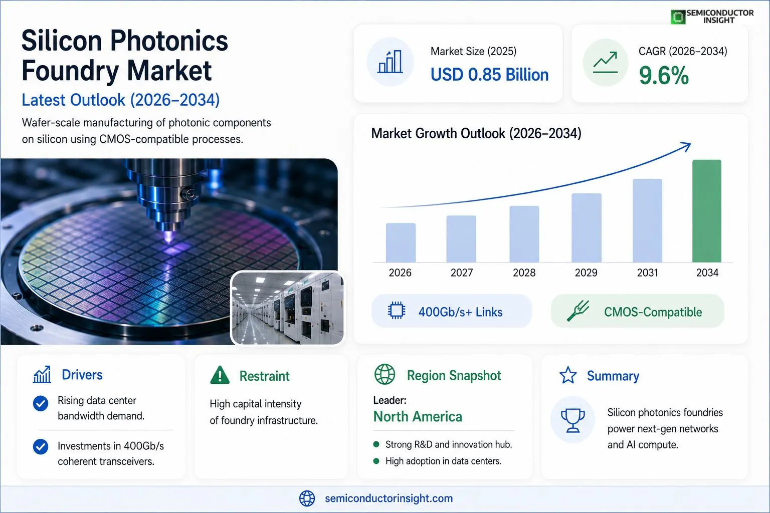
Global silicon photonics foundry market size was valued at USD 0.85 billion in 2025. The market is projected to grow from USD 0.95 billion in 2026 to USD 2.10 billion by 2034, exhibiting a CAGR of 9.6% during the forecast period.
Silicon photonics foundries provide wafer‑scale manufacturing services that integrate optical components,such as waveguides, modulators, and detectors,directly onto silicon substrates using CMOS‑compatible processes. This enables high‑density, low‑cost optical interconnects for data centers, telecommunications, and emerging AI accelerators.The market is accelerating because hyperscale data‑center expansion demands bandwidth beyond electrical limits, while telecom operators invest heavily in coherent transceivers for 400 Gb/s per wavelength links. Furthermore, advances in heterogeneous integration and government R&D subsidies are lowering entry barriers for new entrants.
MARKET DRIVERS
Growing Data Center Bandwidth Demand
The rapid expansion of cloud services and hyperscale data centers is creating a critical need for higher‑speed, lower‑power interconnects. Silicon photonics enables optical links that surpass 400 Gb/s per lane, offering a scalable solution that aligns with silicon photonics foundry market’s growth trajectory.
Advancements in Integrated Photonic Manufacturing
Recent breakthroughs in wafer‑scale integration and CMOS‑compatible processes have improved yield and reduced cycle time. These technical gains lower the overall cost of photonic components, making foundry services more attractive to telecom and automotive OEMs.
➤ “The convergence of data‑intensive workloads and mature silicon photonics processes is reshaping the communications ecosystem.”
Strategic partnerships between chip designers and dedicated photonic foundries are accelerating time‑to‑market, reinforcing silicon photonics foundry market as a cornerstone of next‑generation networking infrastructure.
MARKET CHALLENGES
Manufacturing Complexity and Yield
Integrating high‑precision waveguides with electronic circuitry requires sub‑nanometer alignment, which can lead to variable yields across production lots. Addressing these process nuances remains a significant hurdle for scaling silicon photonics foundry market.
Other Challenges
Cost Sensitivity
Despite efficiency gains, the capital expense of photonic tooling and the need for specialized testing infrastructure keep unit costs higher than traditional silicon electronics, limiting adoption in price‑sensitive segments.
MARKET RESTRAINTS
Capital Intensity of Foundry Infrastructure
Establishing a dedicated silicon photonics fab requires multi‑billion‑dollar investments in lithography, etching, and packaging equipment. This financial barrier restricts the number of viable players, constraining Silicon Photonics Foundry Market expansion to well‑funded incumbents.
MARKET OPPORTUNITIES
Emerging Applications in AI Accelerators
AI accelerators demand ultra‑high‑bandwidth, low‑latency interconnects to move massive data sets between processing cores. Silicon photonics offers a pathway to meet these requirements, opening a significant growth avenue for silicon photonics foundry market as AI hardware ecosystems mature.
Silicon Photonics Foundry Market Trends
Wafer‑Scale Integration Enables High‑Density Optical Links
The wafer‑scale manufacturing model adopted by leading foundries is reshaping optical interconnect strategies. By embedding waveguides, modulators and photodetectors directly onto silicon wafers using CMOS‑compatible processes, suppliers can deliver high‑density link portfolios at cost points that compete with electrical alternatives. This capability aligns precisely with the bandwidth surge required by hyperscale data‑center operators, where optical channels exceeding 400 Gb/s per wavelength are becoming routine. The trend reduces package count, improves thermal management and shortens time‑to‑market for AI‑accelerator modules. Consequently, silicon photonics foundry market is witnessing a migration from prototype runs to multi‑project wafer (MPW) campaigns that serve diverse OEMs within a single production cycle. The adoption of shared MPW runs also lowers non‑recurring engineering costs, allowing startups to qualify silicon photonic designs without committing to full‑scale tape‑out. In addition, the standardized process design kits (PDKs) released by the major foundries simplify layout verification, which accelerates the migration from laboratory prototypes to production‑ready modules.
Other Trends
Heterogeneous Integration and Substrate Innovation
Heterogeneous integration is accelerating as foundries incorporate III‑V epitaxial layers and specialty substrates onto silicon platforms. This approach expands the functional palette beyond passive routing, enabling on‑chip lasers and high‑speed amplifiers that meet the stringent power‑budget of next‑generation transceivers. Government R&D subsidies in several regions have lowered the entry barrier for smaller design houses, fostering a broader ecosystem of niche applications such as quantum‑photonics testbeds and remote‑sensing lidar. The resultant design flexibility encourages a shift from monolithic silicon photonics to modular architectures where best‑in‑class materials are co‑located on a common wafer, improving performance while preserving the cost advantages of volume manufacturing. The increased fab capacity, driven by investments in 300 mm silicon photonics lines, shortens the lead time from design lock‑step to silicon release. Moreover, the collaborative ecosystem between tool vendors and foundries improves design‑for‑manufacturability guidelines, further reducing risk for customers entering the platform.
Telecommunications Drivers and Coherent Transceiver Adoption
The telecommunications sector remains a critical catalyst, with operators investing heavily in coherent transceiver modules that support 400 Gb/s per wavelength links across long‑haul and metro networks. Foundry services now include standardized driver‑receiver IP blocks and validated packaging options that streamline deployment timelines. As network operators pursue 5G and beyond, the demand for scalable, low‑latency optical back‑haul intensifies, reinforcing the strategic importance of silicon‑based photonic foundry capabilities. These dynamics collectively strengthen silicon photonics foundry market’s role as an enabling platform for both data‑center expansion and next‑generation telecom infrastructure. Looking ahead, the convergence of silicon photonics with emerging 6G wireless back‑haul concepts and edge‑AI workloads suggests a sustained growth trajectory. Foundry roadmaps that integrate advanced packaging, such as fan‑out wafer‑level packaging, will be critical to meet the scaling demands of future network topologies.
COMPETITIVE LANDSCAPEKey Industry Players
Silicon Photonics Foundry Market: Accelerating Demand and Technological Convergence
silicon photonics foundry market is currently anchored by a few large-scale CMOS‑compatible manufacturers that dominate wafer‑scale production. Intel’s Custom Foundry Services leads the segment, leveraging its 14 nm and 7 nm process nodes to integrate waveguides, modulators and photodetectors directly on silicon, thereby supporting hyperscale data‑center bandwidth growth. GlobalFoundries follows closely, offering a dedicated silicon photonics platform that emphasizes cost‑effective high‑volume runs for telecom operators targeting 400 Gb/s coherent links. These two players together capture the majority of the $0.85 billion market in 2025, benefitting from deep R&D investments and established supply‑chain relationships that reinforce a tier‑one market structure.Beyond the tier‑one leaders, a diverse set of niche founders adds depth and specialization to the ecosystem. Tower Semiconductor (formerly TowerJazz) provides specialty process options for low‑loss waveguides, while X‑FAB Silicon Foundries focuses on silicon‑on‑insulator (SOI) platforms for AI accelerator interconnects. AIM Photonics operates a dedicated photonic foundry that caters to startups and research institutions, emphasizing rapid prototyping. Rockley Photonics and SillOptics target integrated photonic‑electronic solutions for edge computing, and Lumentum supplies advanced modulators through partnership agreements with larger fabs. This layered competitive landscape ensures both high‑volume capacity and agile, application‑specific innovation, driving the projected CAGR of 9.6 % through 2034.
List of Key Silicon Photonics Foundry Companies Profiled
- Intel Corporation
- GlobalFoundries Inc.
- Tower Semiconductor Ltd.
- X‑FAB Silicon Foundries
- AIM Photonics
- Rockley Photonics
- SillOptics
- Lumentum Holdings Inc.
- EPiq Silicon Photonics Foundry
- Invisio Labs
- Photonics Foundry (PFO)
- Ampleon Technologies
- TSMC (Emerging Silicon Photonics Platform)
- Vanguard Photonics
- Nanophotonic Solutions
Segment Analysis:
| Segment Category | Sub-Segments | Key Insights |
| By Type |
|
Integrated Photonic Modules are gaining traction because they enable customers to acquire complete optical subsystems that are ready for deployment, reducing design complexity and time‑to‑market.
|
| By Application |
|
Data Center Interconnects dominate the application landscape due to the relentless demand for higher bandwidth and energy‑efficient signaling.
|
| By End User |
|
Hyperscale Cloud Providers steer the market direction by seeking ultra‑high‑capacity optical solutions that can be seamlessly scaled.
|
| By Integration Approach |
|
Heterogeneous Integration emerges as the leading approach because it allows the combination of best‑in‑class materials within a single silicon platform.
|
| By Business Model |
|
Fabless Design Services dominate the business‑model landscape by allowing customers to focus on architecture while leveraging the foundry’s manufacturing expertise.
|
Regional Analysis: North America
United States
The expansion of data centers and the increasing demand for high-speed networking are primary drivers for silicon photonics foundry market in the US. Advancements in optical interconnects are crucial for meeting the bandwidth requirements of modern applications.
Ongoing research in silicon photonics integration, packaging, and testing is enabling the development of more efficient and cost-effective foundry services. Innovations in laser diodes, modulators, and detectors are key areas of focus.
The US market features a mix of established and emerging silicon photonics foundry players, alongside major semiconductor manufacturers expanding their offerings. Competition centers on technology leadership, cost competitiveness, and service quality.
The integration of silicon photonics with other semiconductor technologies presents significant opportunities for growth in the US. Expanding into new application areas, such as automotive and consumer electronics, will also drive market expansion.
Europe
Europe represents a growing market for the Silicon Photonics Foundry industry. With strong emphasis on innovation and a well-established industrial base, European nations are investing in silicon photonics for various applications, including high-performance computing, data communication, and industrial automation. The region’s focus on sustainable technologies and energy efficiency further contributes to the demand for silicon photonics solutions.
Asia-Pacific
Asia-Pacific is poised for substantial expansion in silicon photonics foundry market. Countries like China, Japan, and South Korea are witnessing rapid growth in their respective electronics and telecommunications sectors, creating significant demand for high-bandwidth connectivity and advanced computing. Government initiatives promoting domestic semiconductor manufacturing and technological self-reliance are accelerating the growth of the foundry ecosystem in the region.
South America
South America presents a nascent but promising market for silicon photonics foundries. Growing investments in telecommunications infrastructure and increasing adoption of cloud services are expected to drive demand for advanced optical interconnects. The region’s potential lies in capitalizing on the increasing need for high-speed data transmission and cost-effective communication solutions.
Middle East & Africa
The Middle East and Africa represent emerging markets with potential for growth in the Silicon Photonics Foundry sector. Increasing investments in infrastructure development, particularly in telecommunications and data centers, are expected to create demand for silicon photonics solutions. The region’s focus on digital transformation and the adoption of advanced technologies will further contribute to market expansion.
Report Scope
This market research report provides a comprehensive analysis of the Silicon Photonics Foundry Market , covering the forecast period 2026–2034. It offers detailed insights into market dynamics, technological advancements, competitive landscape, and key trends shaping the industry.
Key focus areas of the report include:
- Market Overview: The report begins with an overview outlining its current market scenario, key growth indicators, and industry transformation drivers. It discusses macroeconomic factors, demand–supply balance, regulatory landscape, and the strategic role of semiconductors in powering advancements across industries such as automotive, telecommunications, consumer electronics, and industrial automation.
- Market Size & Forecast: Historical data and future projections for revenue, unit shipments, and market value across major regions and segments.
- Segmentation Analysis: Detailed breakdown by product type, technology, application, and end-user industry to identify high-growth segments and investment opportunities.
- Regional Insights: Insights into market performance across North America, Europe, Asia-Pacific, Latin America, and the Middle East & Africa, including country-level analysis where relevant.
- Competitive Landscape: Profiles of leading market participants, including their product offerings, R&D focus, manufacturing capacity, pricing strategies, and recent developments such as mergers, acquisitions, and partnerships.
- Technology Trends & Innovation: Assessment of emerging technologies, integration of AI/IoT, semiconductor design trends, fabrication techniques, and evolving industry standards.
- Market Drivers & Restraints: Evaluation of factors driving market growth along with challenges, supply chain constraints, regulatory issues, and market-entry barriers.
- Stakeholder Insights: Insights for component suppliers, OEMs, system integrators, investors, and policymakers regarding the evolving ecosystem and strategic opportunities.
FREQUENTLY ASKED QUESTIONS:
What is the current market size of Silicon Photonics Foundry Market?
-> silicon photonics foundry market was valued at USD 0.85 billion in 2025 and is expected to reach USD 2.10 billion by 2034.
What is the projected CAGR for the forecast period?
-> The market exhibits a compound annual growth rate of 9.6% from 2026 to 2034.
What are the primary growth drivers for the market?
-> Key drivers include hyperscale data‑center bandwidth demand, telecom operators’ investment in 400 Gb/s coherent transceivers, advances in heterogeneous integration, and government R&D subsidies lowering entry barriers.
Which applications are fueling market expansion?
-> Rapid adoption in data‑center optical interconnects, high‑speed telecommunications links, and emerging AI accelerator modules are the main application pillars.
What is the forecasted market value for 2026?
-> The market is projected to reach USD 0.95 billion in 2026, marking the early phase of the growth trajectory.

Get Sample Report PDF for Exclusive Insights
Report Sample Includes
- Table of Contents
- List of Tables & Figures
- Charts, Research Methodology, and more...
 Download Sample Report PDF


