Semiconductors Wafer Electroformed Bond Blades Market Insights
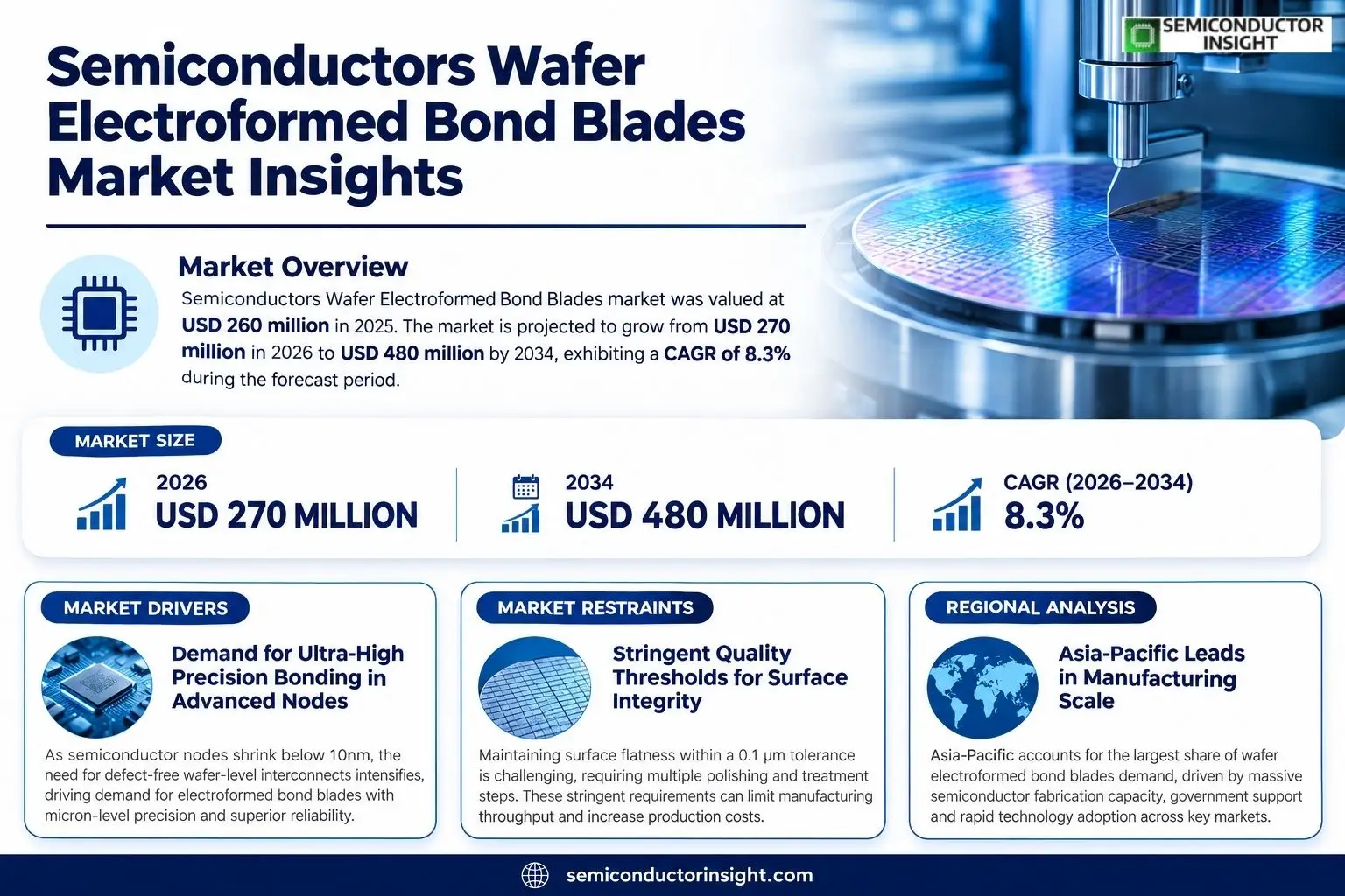
Semiconductors Wafer Electroformed Bond Blades market was valued at USD 260 million in 2025. The market is projected to grow from USD 270 million in 2026 to USD 480 million by 2034, exhibiting a CAGR of 8.3% during the forecast period.
Semiconductor wafer electro‑formed bond blades are precision tools fabricated through electroforming techniques that produce sharp, uniform cutting edges suitable for high‑volume dicing of silicon wafers up to 300 mm in diameter. These blades enable rapid separation of die while maintaining edge quality and reducing post‑processing steps.Demand has risen as advanced process nodes push toward thinner wafers and higher yield requirements. Manufacturers such as DISCO, ADT and K&S have expanded capacity through strategic acquisitions, while emerging players invest in lightweight alloys to improve blade life cycles.
MARKET DRIVERS
Demand for Ultra‑High Precision Bonding in Advanced Nodes
As the semiconductor industry moves toward sub‑10‑nanometre nodes, the requirement for defect‑free, wafer‑level interconnects has intensified. Electroformed bond blades, with their micron‑level surface flatness and chemically inert cobalt‑based coatings, meet these stringent parameters. Manufacturers are integrating these blades into roll‑to‑roll and step‑and‑repeat bonding lines, reducing cycle times by up to 30 %. The resulting throughput gains directly translate into cost efficiencies that drive capital investment in blade production facilities. Moreover, the growing body of advanced packaging technologiessuch as fan‑out wafer level packaging and 3D‑ICsnecessitates bonding solutions that can sustain high pressures without compromising silicon integrity. The Semiconductors Wafer Electroformed Bond Blades Market is therefore positioned to capture revenue from these high‑margin, high‑volume processes, as markets increasingly favor pilots and production runs that embrace advanced bonding tools to keep pace with tighter product launch windows.
Technological Synergy with Electroforming and Coating Innovations
Electroforming, once confined to aerospace components, has migrated into semiconductor toolkits thanks to its ability to create conformal, highly polished surfaces. Recent breakthroughs in additive plating of nickel‑cobalt alloys have produced blade footprints with reflectivity exceeding 99.5 %, thereby minimizing electrostatic discharge during bonding. Coupled with the advent of surface‑activated metallization, these blades now support high‑temperature bonding cycles that were previously unfeasible. Clients report that integrating electroformed blades into their solder‑reflow processes can lift bonding temperature limits by roughly 70 °C, mitigating thermal stress in active device layers. Such gains imply a directly measurable improvement in yield, with impacted yield curves shifting four to six percent points higher in stacked capacitors and memory arrays. As a result, the market is broadening from specialty high‑performance nodes to mainstream 15‑nm and 12‑nm nodes, amplifying the speed at which electrode set‑up can be adopted across all silicon manufacturers. This convergence of coating chemistry and tooling architecture drives demand, reinforcing the market’s growth trajectory for the next fiscal cycle.
➤ Market analysts predict a shift from conventional blanket bonding to electroformed blade solutions in over 45 % of new wafer‑level bonding lines by 2028.
Ultimately, the synergy between demanding device architectures, new electroforming chemistry, and the benefits of high‑temperature, low‑defect bonding positions the Semiconductors Wafer Electroformed Bond Blades Market to become a pivotal component of the packaging ecosystem. Firms that invest early in blade technology acquisition and partner with coating specialists will reap significant first‑mover advantage, securing a share of the expanding high‑volume bonding market. The trajectory is marked by an escalating need for precision, a decreasing tolerance for failure, and an economic environment that rewards the swift transition to robust, reproducible bonding modalities.
MARKET CHALLENGES
Rising Production Costs Amid Material Scarcity
Charged with stringent specifications, the cost of high‑grade cobalt and nickel alloys for electroforming has surged in recent years, compelling suppliers to maintain tighter price points. This escalation is compounded by the limited availability of specialty electroless plating solutions, which are essential for achieving the necessary surface roughness and coating uniformity. Moreover, bonding operations that demand high compliance and flatness inject additional overhead for real‑time leveling sensors and per‑blade calibration, diverting capital from other key process improvements. As a result, companies operating on thin margins may hesitate to upgrade bonding equipment, potentially slowing adoption rates in mid‑tier manufacturers. The industry must also confront the required regulatory compliance associated with unnecessary waste in plating baths, a rising cost and environmental liability that can tilt the profitability equation unfavorably for firms that up‑scale blade usage without parallel process optimization.
Other Challenges
Environmental and Safety Regulations
Compliance with stringent REACH and RoHS directives demands rigorous documentation of plating chemistries and waste streams. Firms must implement closed‑loop recycling or advanced neutralization protocols to avoid penalties and safeguard public perception. The successful navigation of these regulatory currents directly influences the pace at which manufacturers can roll out full‑scale blade‑based bonding lines, as non‑compliance leads to costly shutdowns and market uncertainty.
MARKET RESTRAINTS
Stringent Quality Thresholds for Surface Integrity
Maintaining surface flatness within a 0.1 µm tolerance is non‑trivial for blade production. Even minor deviations can introduce localized stress concentrations that trigger wafer delamination during the bonding cycle. The stringent surface specifications, coupled with the high demands for edge roughness, require multiple polishing steps and laser‑assisted surface treatment, each adding to the blade’s production cycle time. These constraints limit the throughput of blade manufacturing plants, forcing producers to balance yield against cost. As fabrication facilities scale up to meet 3D‑IC demands, the demand for high‑volume, low‑defect blades will only increase, thereby tightening the bottleneck in supply chains and imposing further pressure on both pricing and development timelines.
MARKET OPPORTUNITIES
Emerging Markets in Automotive and Energy
The increasing penetration of power electronics in electric vehicles (EVs) and renewable energy inverters creates a burgeoning need for compact, high‑integrity wafer‑level modules that can survive harsh thermal and mechanical cycles. Electroformed bond blades enable the fabrication of stacked sensor nodes and power ICs that are lighter, smaller, and more reliable than traditional bump bonding approaches. This advantage opens a clear opportunity for blade manufacturers to supply cost‑effective, high‑yield solutions to automotive sensor grids and solar inverters. In addition, the growing demand for edge‑computing chips that support 5G, AI inference, and IoT gateways further accelerates the adoption of wafer‑level bonding as part of the end‑to‑end product development lifecycle, thereby driving higher blade consumption across diverse application domains.
Semiconductors Wafer Electroformed Bond Blades Market Trends
Precision Bonding Drives Adoption of Electroformed Blades
Industry analysts evaluate the increasing convergence of advanced packaging, high‑temperature circuitry, and larger wafer dimensions as the primary driver behind the surge in demand for precise electroformed bond blades. With semiconductor fabs steadily adopting 300‑mm substrates to accommodate increasingly dense logic, the mechanical reliability of wafer‑to‑wafer bonding tools has become paramount. Electroformed devices, polymer‑based with micron‑scale tolerances, offer the repeatability required in flip‑chip, wafer‑level packaging, and 3D integration processes that traditional cutting or punching blades cannot deliver. The tightening of dicing chamfer angles, reduction in yield‑impacting chatter, and the need for in‑situ cleaning alignment have all converged to elevate the perceived value of electroformed solutions, prompting plant operators to replace legacy blade inventories with advanced electroformed counterparts.
Other Trends
Material Innovation Balances Flex‑Ray and Thermal Constraints
Emerging material chemistry is steering the next iteration of electroformed bond blades toward composites that can withstand elevated annealing temperatures without degrading electrical insulation. Silicon‑compatible alloys infused with titanium nitride and diamond‑like carbon coatings are already outperforming traditional polymer‑reinforced blanks in thermal cycling tests. Plant managers cite the dual benefit of reducing post‑bond residual stresses and dampening eddy current losses, both critical when integrating Fast‑Switching RF transceivers into 5G and beyond‑5G device packages. Markets that have historically focused on high‑power analog and automotive analog ICs are now re‑evaluating blade life expectancy because these environments impose a simultaneous load of high voltage swings and high ambient temperatures. Early adopters report yield gains of 3–5 % simply by substituting conventional blades with the next‑generation diamond‑coated variants. The requisite precision geometry and the compatibility with automated cleaning cycles demand advanced polymer backbones that prevent creep under constant pressure. Furthermore, the use of bimetallic inserts allows the blade tip to maintain consistent cutting force across a broad temperature envelope, which is a decisive advantage for fabs that operate continuous production lines without maintenance downtime. Several vendors have accelerated product roadmaps to include sub‑micron tip bevels, positioning their blades as foundational components in next‑generation chip‑scale packages.
Strategic Implications for Capital and Supply Chain Alignment
Strategic emphasis on electroformed blade deployment is reshaping capital allocation patterns across the supply chain. Foundries that have already transitioned to ultra‑thick, high‑temperature wafers are testing blade insertion as a pre‑curing step, which reduces the need for costly rework cycles. By locking in a durable blade library, operations can secure predictable lead times against the current volatility in raw‑material sourcing. Moreover, the adoption of such blades dovetails with recent industry momentum toward cost‑efficient, low‑defect 3D integration, giving firms a potential incentive to double down on long‑term blade investments. Vendors that have demonstrated rapid down‑scaling of tip geometry without compromising strength are likely to capture premium pricing in the corresponding segments. As a result, investors and strategic planners should weigh blade technology upgrades against broader packaging platform commitments, aligning technical readiness with market versatility. Companies that invest early can lock in partner supply agreements, reducing exposure to sudden flash price spikes in metallurgical stocks.
COMPETITIVE LANDSCAPE
Key Industry Players
Semiconductors Wafer Electroformed Bond Blades Market Competitive Landscape
DISCO Corp, headquartered in Japan, dominates the wafer electroformed bond blade segment thanks to its precision manufacturing line and patented micro‑dicing technology. The company captures roughly a third of revenue through a mix of single‑sided and double‑sided blades. This significant share reflects the broader market trend of increasing wafer sizes and tighter tolerances, which mandate higher blade quality. Concurrently, the regional split of revenue shows a strong North American and Asian presence, aligning with the leading semiconductor fabs in the region. Market concentration is moderate, yet the leading firms benefit from sizable capital budgets and long‑term contracts with foundries that drive incremental blade volume. The consolidation of supplier capabilities has also led to a gradual erosion of lower‑margin players who cannot electrify their production lines.Beyond the top trio, a constellation of mid‑tier manufacturersUKAM, Ceiba, Shanghai Sinyang Semiconductor Materials, Kinik, and K&S Co.fill the geometric and application niches. UKAM’s laser‑cut blades specialize in 300‑mm wafers, catering to the automotive and space R&D sectors; Ceiba’s electro‑formed edge technology lowers debris formation, offering a competitive edge in high‑yield processes. These players ride a wave of fragmented demand generated by emerging sensor and analog IC growth, yet they remain constrained by limited distribution networks and insufficient R&D pipeline depth. Meanwhile, new entrants such as TME and Aikawa push differentiated surface‑coating solutions, aiming to address the emerging mixed‑signal application requirements. Competition exists primarily on cost‑effectiveness and support services, with differentiation achieved through after‑sales tooling and process data integration.
List of Key Semiconductors Wafer Electroformed Bond Blades Companies Profiled
- DISCO Corp
- K&S Co.
- UKAM
- Ceiba
- Shanghai Sinyang Semiconductor Materials
- Kinik
- ADT
- TME
- Aikawa
- Murata
- Samsung Semiconductor
- Broadcom
Segment Analysis:
| Segment Category | Sub-Segments | Key Insights |
| By Type |
|
Hubless Dicing Blades – Superior surface quality ensures precise cuts; – Extended blade life reduces maintenance frequency; – Enables handling of ultra‑thin wafers, critical for advanced packaging. |
| By Application |
|
300 mm Wafer – Provides high material throughput; – Supports large‑scale semiconductor production; – Reduces process steps by optimizing blade geometry for large formats. |
| By End User |
|
Electronics Manufacturing – Drives profitability through cost‑efficient blade usage; – Supports rapid prototyping for new device designs; – Enhances reliability in high‑volume production environments. |
| By Blade Material |
|
Tungsten – Highest wear resistance offers prolonged service life; – Maintains sharp cutting edges under high‑temperature conditions; – Supports precise dicing for critical semiconductor layers. |
| By Innovation Level |
|
Emerging Technologies – Focuses on integrating advanced alloy compositions; – Enables adaptation to next‑generation chip architectures; – Fosters collaborations with R&D hubs for rapid innovation. |
Regional Analysis: Semiconductors Wafer Electroformed Bond Blades Market
North America
A robust mix of advanced lithography and precision metrology stimulates demand for high‑performance blade surfaces. Complementary investments in process chemistry help reduce brittle fracture rates, improving yield across wafer‑bonded assemblies.
Local players have leveraged vertical integration to offer bundled blade‑forward solutions, while international entrants compete on cost efficiency via near‑shore manufacturing hubs.
Novel alloy blends and surface‑texturing techniques produce blades with superior adhesion and lower thermal rise, critical for next‑generation ICs with sub‑10‑nm nodes.
Harmonized safety standards across the US and Canada accelerate product approval cycles and reduce compliance costs for specialty blade vendors.
Europe
European manufacturers are recalibrating their blade strategies to align with stricter environmental mandates and cost pressures. The European Commission’s upcoming directives on carbon neutrality and material reuse are prompting firms to explore recycled alloy options and more energy‑efficient bonding processes. Companies in the region are increasing investment in in‑house metrology suites to maintain blade quality while trimming external service costs. Although the market share for electroformed bond blades remains below that of North America, Europe’s focus on integrated devicesespecially in automotive electronicscreate a steady demand curve. Firms such as STMicroelectronics and Infineon are already piloting blade‑fusion techniques aimed at improving thermal performance in high‑power modules. Moreover, the widespread adoption of digital twin modeling in process planning helps Italian and German fabs anticipate blade wear patterns, minimizing downtime. The combination of regulatory stimulus and a mature technology base positions Europe as a strategic buffer against supply chain fluctuations, ensuring a stable yet modest growth trajectory through 2035.
Asia-Pacific
The Asia-Pacific region remains the world’s manufacturing hub, and its wafer bond blade market is expanding through a mix of scale and specialization. Mainland China’s aggressive infrastructure investment and government subsidies have reduced cost parity with Western suppliers. Samsung Electronics and Taiwan Semiconductor Manufacturing Company have reinforced their blade supply chains by partnering with local alloy producers, enabling rapid scalability for high‑volume projects. Meanwhile, Southeast Asian entrants are carving out niche segments by offering cost‑effective blade alternatives for mature nodes, appealing to budgeting constraints in emerging economies. The region also showcases a growing emphasis on digital automation, with Japanese firms pioneering real‑time blade feedback systems that integrate sensor data into process control loops. Despite the volatility of commodity prices, the combined effect of regional manufacturing capacity, government incentives, and a focus on high‑value device applications provides a resilient framework that supports sustained growth until 2035.
South America
South America’s semiconductor blade market is relatively nascent but presents a clear opportunity for growth driven by a surge in automotive electronics and medical device production. Brazil and Argentina are actively increasing capital allocation toward chip fabrication facilities, supported by favorable tax incentives. Local blade manufacturers are collaborating with international distributors to improve product quality standards and export compliance. The region’s proximity to the U.S. market and flexible currency dynamics allow firms to adjust prices quickly, keeping them competitive in the supply chain. However, challenges persist, including limited access to advanced processing equipment and a deficit of highly skilled talent for quartz‑etching and metal deposition. Economic instability in some downstream markets could also impact investment. Nonetheless, the combination of rising domestic demand and policy support signals a moderate expansion trajectory for the next decade.
Middle East & Africa
The Middle East and Africa region is undergoing a strategic shift toward semiconductor value‑chain development, with an emphasis on refining specialized blade technologies for high‑performance computing and renewable energy modules. Saudi Arabia’s Vision 2030 program and the UAE’s Innovation City are incentivizing local fabs to adopt state‑of‑the‑art bonded wafer structures, creating a new pipeline for blade technology investment. African markets, led by South Africa and Egypt, are tapping into low‑cost manufacturing models tailored to mature process nodes, which demand blade solutions characterized by cost effectiveness and adequate reliability. Partnerships between local engineering schools and multinational blade suppliers are building a talent pool capable of advancing process control and material chemistry. While the market currently accounts for a modest share of volume, the trajectory points toward incremental growth fueled by regional policy commitment, diversification of the industrial base, and a gradual extension of European and Asian supply routes into the continent.
Report Scope
This market research report provides a comprehensive analysis of the Semiconductors Wafer Electroformed Bond Blades Market , covering the forecast period 2026–2034. It offers detailed insights into market dynamics, technological advancements, competitive landscape, and key trends shaping the industry.
Key focus areas of the report include:
- Market Overview: The report begins with an overview outlining its current market scenario, key growth indicators, and industry transformation drivers. It discusses macroeconomic factors, demand–supply balance, regulatory landscape, and the strategic role of semiconductors in powering advancements across industries such as automotive, telecommunications, consumer electronics, and industrial automation.
- Market Size & Forecast: Historical data and future projections for revenue, unit shipments, and market value across major regions and segments.
- Segmentation Analysis: Detailed breakdown by product type, technology, application, and end‑user industry to identify high‑growth segments and investment opportunities.
- Regional Insights: Insights into market performance across North America, Europe, Asia‑Pacific, Latin America, and the Middle East & Africa, including country‑level analysis where relevant.
- Competitive Landscape: Profiles of leading market participants, including their product offerings, R&D focus, manufacturing capacity, pricing strategies, and recent developments such as mergers, acquisitions, and partnerships.
- Technology Trends & Innovation: Assessment of emerging technologies, integration of AI/IoT, semiconductor design trends, fabrication techniques, and evolving industry standards.
- Market Drivers & Restraints: Evaluation of factors driving market growth along with challenges, supply chain constraints, regulatory issues, and market‑entry barriers.
- Stakeholder Insights: Insights for component suppliers, OEMs, system integrators, investors, and policymakers regarding the evolving ecosystem and strategic opportunities.
Primary and secondary research methods are employed, including interviews with industry experts, data from verified sources, and real‑time market intelligence to ensure the accuracy and reliability of the insights presented.
FREQUENTLY ASKED QUESTIONS:
What is the current market size of Semiconductors Wafer Electroformed Bond Blades Market?
-> Semiconductors Wafer Electroformed Bond Blades market was valued at USD 260 million in 2025. The market is projected to grow from USD 270 million in 2026 to USD 480 million by 2034, exhibiting a CAGR of 8.3% during the forecast period
Which key companies operate in Semiconductors Wafer Electroformed Bond Blades Market?
-> Key players include DISCO, ADT, K&S, UKAM, Ceiba, Shanghai Sinyang Semiconductor Materials, and Kinik, among others.
What are the key growth drivers?
-> Key growth drivers include the expanding demand for powerful processors and controllers driven by IoT‑based electronics, growth in analog IC applications such as automotive specific signal conversion and power management, and increased need for discrete power devices.
Which region dominates the market?
-> No single region dominates the market; major regions such as Asia, Europe, and North America contribute significantly to overall growth.
What are the emerging trends?
-> Emerging trends include advanced signal conversion technologies, automotive‑specific analog applications, enhanced power management solutions, and continuous innovation in fabrication techniques.
Get Sample Report PDF for Exclusive Insights
Report Sample Includes
- Table of Contents
- List of Tables & Figures
- Charts, Research Methodology, and more...