Semiconductor Film Market Insights
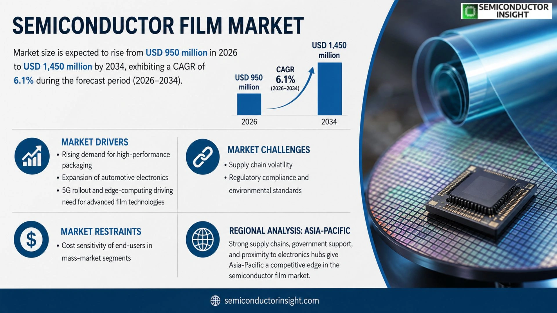
Semiconductor Film market size was valued at USD 850 million in 2025. The market is expected to rise from USD 950 million in 2026 to USD 1,450 million by 2034, exhibiting a CAGR of approximately 6.1% during the forecast period.
Semiconductor film refers to thin protective coatings applied during front‑end and back‑end processes of wafer fabrication. These films shield delicate circuitry from contamination, mechanical stress, and chemical exposure while preserving optical transparency and thermal stability required for advanced lithography.
The upward trajectory is driven by expanding demand for high‑density integrated circuits, increasing adoption of advanced packaging such as fan‑out wafer‑level packaging, and heightened focus on yield improvement across fabs worldwide. Additionally, the shift toward heterogeneous integration intensifies the need for reliable barrier layers, prompting manufacturers like Mitsui Chemicals and Nitto Denko to expand capacity and introduce ultra‑thin (<100 nm) variants.
MARKET DRIVERS
Rising Demand for High‑Performance Packaging
Semiconductor Film market is being propelled by manufacturers’ need for thinner, lighter, and more thermally stable packaging solutions. As chip architectures shrink, traditional substrates struggle to meet the thermal‑dissipation requirements, prompting a shift toward advanced film‑based laminates that can sustain higher power densities while keeping form factors minimal.
Expansion of Automotive Electronics
Electrification and autonomous‑driving features are embedding an ever‑greater number of sensors and power modules in vehicles. This trend compels automotive OEMs to adopt semiconductor films that provide superior flexibility and resistance to vibration, thereby supporting safety‑critical systems without compromising weight targets.
➤ Analysts observe that the convergence of 5G infrastructure rollout and edge‑computing workloads is sharpening the competitive edge of firms that can deliver film technologies with both high dielectric strength and low cost.
These drivers collectively reshape supply strategies; companies that can lock in raw‑material sources while scaling thin‑film production lines are positioned to capture a larger share of the evolving ecosystem.
MARKET CHALLENGES
Supply Chain Volatility
Fluctuations in petrochemical feedstock prices translate directly into cost pressure for film manufacturers. Recent geopolitical tensions have introduced unpredictable lead times, forcing end‑users to reassess inventory buffers and potentially delay product launches.
Other Challenges
Regulatory Compliance
Stringent environmental regulations in Europe and North America demand lower VOC emissions during film production. Compliance frameworks increase capital expenditures and may deter smaller players from entering the market.
MARKET RESTRAINTS
Cost Sensitivity of End‑Users
While advanced films deliver performance benefits, many OEMs remain price‑conscious, especially in mass‑market segments such as consumer electronics. The premium attached to high‑specification films can restrict adoption unless clear ROI is demonstrated through extended device lifespans or reduced system complexity.
MARKET OPPORTUNITIES
Emerging Applications in IoT Devices
IoT deployments demand miniature, power‑efficient modules that can operate reliably in diverse environments. Semiconductor films offering a blend of flexibility, moisture barrier performance, and low dielectric loss are uniquely suited to these applications, opening pathways for niche manufacturers to differentiate their portfolios.
Semiconductor Film Market Trends
Emerging Demand for High‑Performance Protective Films in Advanced Nodes
The push for tighter transistor pitches in leading‑edge logic and analog devices has heightened the need for protective coatings that survive aggressive plasma etch, high‑temperature bake and multiple photolithography cycles. Film suppliers are responding with chemistries that combine low dielectric constant, high mechanical strength and ultra‑clean peel‑off characteristics, allowing manufacturers to preserve wafer integrity without sacrificing yield. As the broader Semiconductor Film Market absorbs more of the IoT‑driven processor rollout, the value placed on defect‑free surfaces has risen, prompting R&D budgets to prioritize abrasion resistance and optical transparency. This technical shift reshapes vendor contracts, as foundry clients now specify film performance metrics alongside traditional material costs.
Other Trends
Shift Toward Thinner Films for Front‑End Process Integration
Across the front‑end workflow, design teams are gravitating to films thinner than 100 nm to reduce topography buildup and minimize pattern distortion during exposure. The thinner stack not only eases focus control for advanced lithography tools but also shortens cycle times, delivering a modest efficiency gain that adds up across high‑volume fabs. However, the move introduces handling challenges; manufacturers must guarantee uniformity across large‑area substrates while preventing puncture or delamination. Consequently, the supply side is investing in precision casting and roll‑to‑roll coating lines capable of sub‑micron thickness control, a trend that is gradually influencing equipment procurement strategies and altering the cost structure of Semiconductor Film market.
Regional Supply‑Chain Realignments Amplify Market Opportunities
Recent trade adjustments have prompted major producers in South Korea, Japan and Taiwan to diversify export routes and augment local capacity, reducing reliance on single‑port logistics. At the same time, North American fabs are tightening partnerships with European specialty‑film firms to secure niche formulations for automotive and aerospace applications. This geographic rebalancing is creating pockets of growth where region‑specific standards,such as higher temperature tolerance for Asian high‑volume manufacturing or stricter environmental compliance for European customers,drive differentiated product lines. For investors, the realignment signals a need to monitor policy shifts and capacity announcements, as they will shape competitive positioning and pricing dynamics within Semiconductor Film market over the next several years.
COMPETITIVE LANDSCAPE
Key Industry Players
Semiconductor Film Market: Competitive Overview
Semiconductor film sector remains anchored by a handful of multinational chemists whose vertical integration grants them control over raw material sourcing, coating technology, and global distribution networks. Mitsui Chemicals leads the field by leveraging its extensive polymer portfolio and deep relationships with wafer fabs, enabling it to capture the bulk of high‑volume protective‑film contracts. Nitto Denko follows closely, distinguished by its advanced optical‑clarity coatings that meet the stringent yield requirements of front‑end fabs. Both firms operate large‑scale production lines in East Asia and maintain subsidiaries in North America and Europe, creating a tiered supply chain that pressures smaller entrants to specialize or form strategic alliances.
Beyond the tier‑one group, a diverse set of specialists contributes niche capabilities that address emerging process nodes and specialty applications. AMC and Harima Chemicals focus on ultra‑thin, low‑stress laminates for sensor and analog IC production. Deep Materials and Shanghai Lanqing have carved out reputations for rapid‑turn custom formulations catering to prototype runs. Hengchuang Material, Koatech, and Tsinghon supply cost‑effective bulk films for back‑end packaging, while Jilin Fine Chemical, Sumitomo Chemical, and Asahi Kasei provide high‑performance barrier layers for automotive and IoT devices. International conglomerates such as DuPont, 3M, and LG Chem round out the ecosystem, offering cross‑industry expertise that blurs traditional market boundaries.
List of Key Semiconductor Companies Profiled
- Mitsui Chemicals
- Nitto Denko
- AMC
- Harima Chemicals
- Deep Materials
- Shanghai Lanqing
- Hengchuang Material
- Koatech
- Tsinghon
- Jilin Fine Chemical
- Sumitomo Chemical
- Asahi Kasei
- DuPont
- 3M
- LG Chem
Segment Analysis:
| Segment Category | Sub-Segments | Key Insights |
| By Type |
|
Thin‑Film Segment is leading because it enables higher pattern fidelity for advanced nodes, it supports flexible manufacturing approaches, and it aligns with industry trends toward miniaturization.
|
| By Application |
|
Front‑end Process Segment dominates due to its critical role in device formation, its influence on yield improvements, and its alignment with emerging logic and analog designs.
|
| By End User |
|
Consumer Electronics Segment leads as manufacturers prioritize higher device reliability, thinner form factors, and faster time‑to‑market.
|
| By [Segment Category 3]] |
|
N/A |
| By [Segment Category 4]] |
|
N/A |
Regional Analysis: Semiconductor Film Market
Asia‑Pacific
The region hosts several high‑volume fabs that specialize in thin‑film deposition, benefiting from economies of scale and advanced process control. Their ability to produce large‑area substrates at consistent quality underpins the supply reliability demanded by tier‑1 device makers.
Corporate and academic partnerships channel substantial resources into next‑generation materials, such as low‑temperature oxides and novel polymer matrices. These collaborations accelerate proof‑of‑concept transitions into pilot lines, shortening the time to market for innovative film technologies.
Integrated logistics corridors link raw‑material producers, wafer manufacturers, and downstream assemblers. This geographic continuity reduces inventory buffers and enhances responsiveness to shifts in demand patterns across consumer electronics.
Streamlined certification procedures and harmonized environmental standards lower compliance costs. Regulatory clarity enables firms to scale operations without encountering prolonged approval cycles that could stall expansion plans.
North America
The North American market remains anchored by a deep pool of engineering talent and a mature ecosystem of equipment suppliers. End‑users prioritize performance consistency and reliability, prompting domestic producers to maintain stringent quality regimes. While cost pressures encourage selective off‑shoring, strategic partnerships with Asian firms allow access to high‑volume capacity without compromising on technical specifications. The region’s emphasis on intellectual property protection also sustains a pipeline of proprietary film formulations aimed at high‑end applications such as aerospace and medical devices.
Europe
European stakeholders focus on sustainability and circular‑economy principles, influencing material selection for semiconductor films. Regulatory frameworks encourage the use of recyclable substrates and low‑emission processes, driving manufacturers to innovate greener chemistries. Collaborative platforms across the EU foster cross‑border projects, blending expertise from optics, materials science, and microelectronics. This approach yields niche solutions tailored for automotive displays and industrial sensors, where durability and environmental compliance are paramount.
South America
In South America, emerging electronics clusters are beginning to explore localized production of semiconductor films to reduce dependence on imports. Government initiatives aim to develop technology parks that attract foreign investment and provide training for a skilled workforce. Early adopters in the region are leveraging these incentives to prototype flexible modules for renewable‑energy monitoring devices, positioning the market for gradual but steady growth.
Middle East & Africa
The Middle East & Africa region exhibits a heterogeneous landscape, with select economies investing heavily in high‑tech infrastructure while others remain nascent. Strategic diversification plans in Gulf states include partnerships with global film manufacturers to establish regional assembly hubs. Meanwhile, African markets are gradually adopting semiconductor films for telecommunications equipment, driven by expanding mobile‑network coverage. Collaboration between multinational firms and local investors is fostering a foundation for longer‑term market development.
Report Scope
This market research report provides a comprehensive analysis of the Semiconductor Film Market , covering the forecast period 2026–2034. It offers detailed insights into market dynamics, technological advancements, competitive landscape, and key trends shaping the industry.
Key focus areas of the report include:
- Market Overview: The report begins with an overview outlining its current market scenario, key growth indicators, and industry transformation drivers. It discusses macroeconomic factors, demand–supply balance, regulatory landscape, and the strategic role of semiconductors in powering advancements across industries such as automotive, telecommunications, consumer electronics, and industrial automation.
- Market Size & Forecast: Historical data and future projections for revenue, unit shipments, and market value across major regions and segments.
- Segmentation Analysis: Detailed breakdown by product type, technology, application, and end-user industry to identify high-growth segments and investment opportunities.
- Regional Insights: Insights into market performance across North America, Europe, Asia-Pacific, Latin America, and the Middle East & Africa, including country-level analysis where relevant.
- Competitive Landscape: Profiles of leading market participants, including their product offerings, R&D focus, manufacturing capacity, pricing strategies, and recent developments such as mergers, acquisitions, and partnerships.
- Technology Trends & Innovation: Assessment of emerging technologies, integration of AI/IoT, semiconductor design trends, fabrication techniques, and evolving industry standards.
- Market Drivers & Restraints: Evaluation of factors driving market growth along with challenges, supply chain constraints, regulatory issues, and market-entry barriers.
- Stakeholder Insights: Insights for component suppliers, OEMs, system integrators, investors, and policymakers regarding the evolving ecosystem and strategic opportunities.
Primary and secondary research methods are employed, including interviews with industry experts, data from verified sources, and real-time market intelligence to ensure the accuracy and reliability of the insights presented.
FREQUENTLY ASKED QUESTIONS:
What is the current market size of Semiconductor Film Market?
-> Semiconductor Film market is expected to rise from USD 950 million in 2026 to USD 1,450 million by 2034, exhibiting a CAGR of approximately 6.1%
Which key companies operate in Semiconductor Film Market?
-> Key players include Mitsui Chemicals, Nitto Denko, AMC, Harima Chemicals, Deep Materials, Shanghai Lanqing, Hengchuang Material, Koatech, Tsinghon, among others.
What are the key growth drivers?
-> Key growth drivers include expanding demand for protective films in semiconductor manufacturing, growth of IoT‑based electronics, increased adoption of advanced packaging, and rising need for high‑performance analog and sensor ICs.
Which region dominates the market?
-> Asia dominates Semiconductor Film market, driven by strong semiconductor production in China, Japan, and South Korea, while other regions follow.
What are the emerging trends?
-> Emerging trends include integration of flexible protective films for advanced packaging, AI‑enabled film inspection technologies, and development of environmentally friendly (low‑VOC) film materials.

Get Sample Report PDF for Exclusive Insights
Report Sample Includes
- Table of Contents
- List of Tables & Figures
- Charts, Research Methodology, and more...
 Download Sample Report PDF