Semiconductor Dry Strip Equipment Market Insights
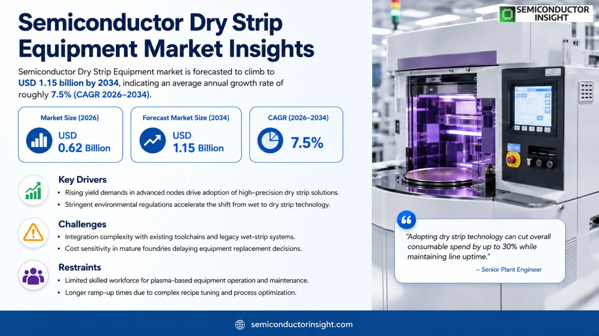
Semiconductor Dry Strip Equipment market was valued at USD 620 million in 2025 and is forecasted to climb to USD 1.15 billion by 2034, indicating an average annual growth rate of roughly 7.5 % throughout the horizon.
Dry strip refers to the process of eliminating masking layers from a wafer after patterning has been completed; the goal is rapid removal while preserving underlying surface integrity.
The expansion reflects rising demand for high‑performance computing chips, AI accelerators and advanced packaging, all of which increase wafer throughput requirements. Moreover, regional equipment spending patterns, particularly strong growth in China, Taiwan and South Korea, support higher adoption rates for fully automatic dry‑strip systems.
MARKET DRIVERS
Rising Yield Demands in Advanced Nodes
The push toward sub‑10 nm technologies forces fab operators to tighten defect tolerances. Semiconductor Dry Strip Equipment that can remove photoresist without contaminating the wafer surface becomes indispensable, because even microscopic residues jeopardize cycle yield. Manufacturers are therefore allocating a larger share of capex to equipment that offers tighter process windows and repeatable performance.
Stringent Environmental Regulations
Legislative scrutiny on wet chemistry waste has accelerated the shift to dry strip solutions. Facilities that replace hazardous solvents with plasma‑based processes benefit from lower disposal costs and a smaller regulatory footprint, positioning dry‑strip platforms as a compliance‑friendly alternative.
➤ “Adopting dry strip technology can cut overall consumable spend by up to 30 % while maintaining line uptime,” notes a senior plant engineer.
These dynamics compel equipment vendors to broaden their product portfolios, integrating real‑time monitoring and AI‑enhanced control loops that further improve throughput and reduce manual interventions.
MARKET CHALLENGES
Integration Complexity with Existing Toolchains
Many fabs operate heterogeneous process lines where legacy wet‑strip stations coexist with newer dry‑strip modules. Aligning cycle times, gas handling infrastructure, and maintenance schedules across such mixed environments creates scheduling friction and demands customized engineering support.
Other Challenges
Cost Sensitivity in Mature Foundries
Mature‑node manufacturers prioritize cost per wafer over marginal performance gains, making them reluctant to replace proven wet‑strip assets until the total cost of ownership advantage of dry‑strip systems is unequivocally demonstrated.
MARKET RESTRAINTS
Limited Skilled Workforce
Operating plasma‑based dry strip equipment requires specialized knowledge of process chemistry, vacuum technology, and equipment diagnostics. The scarcity of technicians trained in these niches slows adoption, as fabs must invest in upskilling programmes or rely on vendor‑provided service contracts.
Additionally, the steep learning curve associated with tuning recipes for diverse wafer architectures can extend ramp‑up periods, nudging some operators to postpone upgrades.
Given these workforce constraints, equipment makers are increasingly bundling training modules and remote support packages to mitigate the talent gap.
MARKET OPPORTUNITIES
Modular Architecture for Customized Deployments
Vendors that design dry‑strip platforms with interchangeable plasma sources and gas‑delivery modules enable fabs to tailor configurations to specific product lines. This flexibility reduces upfront capital outlay and offers a clear upgrade path as process requirements evolve.
Emerging AI‑driven recipe optimization tools present another growth avenue. By continuously correlating process parameters with defect data, these systems can cut trial‑and‑error cycles, delivering faster time‑to‑market for new semiconductor generations.
Finally, expansion into specialty markets, such as MEMS and power‑device manufacturing, where thin‑film cleaning is critical, broadens the addressable base for the Semiconductor Dry Strip Equipment Market beyond traditional logic and memory fabs.
Semiconductor Dry Strip Equipment Market Trends
Shift Toward Fully Automatic Stripping
The adoption of fully automatic dry‑strip platforms is accelerating as wafer designs become denser and cycle time pressure intensifies. Automation eliminates manual interventions that can introduce particle contamination, while precise endpoint detection curtails over‑etch and pattern damage. Manufacturers that upgrade to fully automatic lines report yield improvements of up to 12 % on high‑performance computing (HPC) and 5G chips, where any defect translates directly into costly re‑work. For suppliers, this trend reshapes the product roadmap: equipment families now emphasize modular control software, integrated metrology, and rapid change‑over capabilities to match the speed of advanced lithography.
Other Trends
Regional Market Realignment
Asia retains a commanding presence, accounting for more than 70 % of the overall semiconductor equipment spend in 2022, with China, Taiwan, and South Korea leading the charge. This concentration reflects robust fab expansions backed by government incentives and a mature supply ecosystem. In contrast, North America, Europe, and Japan together hold roughly 23 % of the market, focusing on niche high‑value nodes and specialty applications such as automotive safety processors. The divergence creates a strategic dilemma for equipment vendors: they must calibrate investment between high‑volume, cost‑sensitive Asian fabs and lower‑volume, technology‑intensive Western sites.
Integration of AI‑Enabled Process Control
Artificial‑intelligence algorithms are being embedded directly into dry‑strip controllers to predict endpoint with sub‑second accuracy. By analyzing real‑time plasma emission spectra and wafer temperature trends, the system can adjust power and gas flow pre‑emptively, reducing cycle time by 5‑8 % while safeguarding critical layers. This capability aligns with the broader push for smarter fabs, where predictive maintenance and closed‑loop control are standard. Vendors that successfully commercialize AI‑augmented dry‑strip solutions are likely to secure a larger share of the Semiconductor Dry Strip Equipment Market, as fab managers seek to lower total cost of ownership and improve throughput without compromising defect density.
COMPETITIVE LANDSCAPE
Key Industry Players
Semiconductor Dry Strip Equipment – Competitive Overview 2024‑2031
The dry‑strip segment is dominated by a handful of large‑scale manufacturers that have leveraged deep process‑integration expertise and extensive fab‑service networks. Lam Research and Tokyo Electron occupy the upper tier, each offering both semi‑automatic and fully automatic systems that cater to high‑volume logic and memory fabs. Their ability to embed advanced plasma‑control algorithms into equipment platforms gives them a pricing advantage and secures long‑term service contracts with the leading foundries in Taiwan, South Korea and China. Both firms have expanded their product portfolios through targeted acquisitions, allowing them to address niche applications such as advanced packaging and 3‑D‑IC stripping. The concentration of revenue among these two players means that strategic moves, whether a new generation of high‑throughput tools or a shift toward modular architectures, ripple through the entire supply chain, influencing component pricing, spare‑part inventories and after‑sales support structures.
Beyond the top tier, a diverse group of midsize and specialist firms is shaping the competitive environment. ULVAC and SCREEN Holdings differentiate themselves through bespoke plasma‑source designs that prioritize low‑damage removal for thin‑film and sensor applications. Chinese entrants such as Beijing E‑Town, PSK and NAURA have capitalized on domestic fab expansion, providing cost‑effective equipment that aligns with government incentives for local sourcing. European players like TES and Axcelis focus on niche markets, automotive electronics and power‑device fabrication, where reliability and cycle‑time guarantees command premium pricing. Applied Materials, while traditionally associated with etch and deposition, has entered the dry‑strip arena with a hybrid tool that merges its lithography expertise with plasma processing, aiming to capture a share of the emerging high‑performance‑computing fabs. Collectively, these companies create a layered competitive fabric where scale, customization and regional policy interplay to define market share dynamics.
List of Key Semiconductor Dry Strip Equipment Companies Profiled
- Tokyo Electron Ltd.
- SCREEN Holdings Co., Ltd.
- ULVAC, Inc.
- Lam Research Corporation
- Hitachi High‑Tech Corporation
- Beijing E‑Town
- PSK (Shanghai) Technology Co., Ltd.
- TES GmbH
- NAURA Technology Co., Ltd.
- Applied Materials, Inc.
- Axcelis Technologies, Inc.
- AMD – OEM integration unit
- Kobelco (Kobe Steel) – Specialized tooling division
- Systec, Inc.
- Samsung Electronics – equipment development arm
Segment Analysis:
| Segment Category | Sub-Segments | Key Insights |
| By Type |
|
Fully Automatic
|
| By Application |
|
Industrial
|
| By End User |
|
Foundries
|
| By Technology |
|
Plasma‑based Dry Strip
|
| By Process Integration |
|
Front‑End‑of‑Line
|
Regional Analysis: Semiconductor Dry Strip Equipment Market
North America
The bulk of wafer‑fabrication capacity resides in Silicon Valley, Texas, and the Pacific Northwest, creating a dense hub where equipment vendors can co‑locate pilot lines. This geographic clustering reduces logistics overhead and enables real‑time feedback loops between fabs and OEMs, accelerating iterative design of dry strip heads.
Recent geopolitical shifts prompted many North American fabs to diversify critical component sourcing. Domestic production of high‑purity gases and ceramics now underpins a more robust supply chain, shielding the Semiconductor Dry Strip Equipment Market from external bottlenecks and stabilizing lead times.
Strict emissions standards and hazardous‑waste directives have forced equipment makers to adopt closed‑loop plasma chambers. Compliance requirements act as a catalyst for innovation, prompting designers to embed advanced monitoring sensors that improve process repeatability while meeting environmental thresholds.
Venture capital and government grants target low‑damage etch and strip technologies, reflecting confidence in the market’s long‑term upside. Funding streams accelerate prototype development, allowing early‑stage firms to scale solutions that address the industry’s demand for finer pattern fidelity.
Europe
European fabs, particularly in Germany and the Netherlands, are leveraging the Semiconductor Dry Strip Equipment Market to meet the EU’s stringent circular‑economy goals. Manufacturers are prioritizing equipment that reduces consumable waste and offers modular upgrades, aligning with policy incentives that reward resource efficiency. Collaboration between equipment vendors and research institutes such as IMEC and CEA fuels a pipeline of plasma‑based stripping techniques tuned for emerging lithography standards. The competitive pressure from Asian players pushes European suppliers to differentiate through advanced process control software, a strategy that resonates with customers seeking to minimize defectivity at sub‑5 nm nodes.
Asia‑Pacific
The Asia‑Pacific region benefits from a confluence of high fab density and aggressive cost‑optimization mandates. In Taiwan, South Korea, and China, equipment manufacturers tailor dry strip solutions to balance throughput with the delicate film thicknesses required for ultra‑thin devices. Local supply chains provide rapid access to specialty gases, while government subsidies for advanced packaging spur investment in multi‑patterning‑compatible strip tools. The market’s evolution here is shaped by the need to sustain volume production without compromising the stringent cleanliness standards demanded by leading foundries.
South America
South America remains a niche but growing participant in the Semiconductor Dry Strip Equipment Market, buoyed by emerging fabrication parks in Brazil and Colombia. These facilities focus on specialty applications such as power‑device production, where precise residue removal directly influences device reliability. Partnerships with North American OEMs enable technology transfer, while local incentives for high‑tech manufacturing help offset the higher capital costs associated with state‑of‑the‑art dry strip equipment.
Middle East & Africa
Middle East & Africa are gradually entering the Semiconductor Dry Strip Equipment Market as regional diversification strategies attract semiconductor investment. In the United Arab Emirates and Saudi Arabia, government‑backed techno‑parks are commissioning pilot lines that demand clean‑room‑grade strip solutions. Early adopters prioritize equipment with low energy consumption to align with sustainability agendas, prompting vendors to showcase modular designs that can be scaled as the local ecosystem matures.
Report Scope
This market research report provides a comprehensive analysis of the Semiconductor Dry Strip Equipment Market , covering the forecast period 2026–2034. It offers detailed insights into market dynamics, technological advancements, competitive landscape, and key trends shaping the industry.
Key focus areas of the report include:
- Market Overview: The report begins with an overview outlining its current market scenario, key growth indicators, and industry transformation drivers. It discusses macroeconomic factors, demand–supply balance, regulatory landscape, and the strategic role of semiconductors in powering advancements across industries such as automotive, telecommunications, consumer electronics, and industrial automation.
- Market Size & Forecast: Historical data and future projections for revenue, unit shipments, and market value across major regions and segments.
- Segmentation Analysis: Detailed breakdown by product type, technology, application, and end-user industry to identify high-growth segments and investment opportunities.
- Regional Insights: Insights into market performance across North America, Europe, Asia-Pacific, Latin America, and the Middle East & Africa, including country-level analysis where relevant.
- Competitive Landscape: Profiles of leading market participants, including their product offerings, R&D focus, manufacturing capacity, pricing strategies, and recent developments such as mergers, acquisitions, and partnerships.
- Technology Trends & Innovation: Assessment of emerging technologies, integration of AI/IoT, semiconductor design trends, fabrication techniques, and evolving industry standards.
- Market Drivers & Restraints: Evaluation of factors driving market growth along with challenges, supply chain constraints, regulatory issues, and market-entry barriers.
- Stakeholder Insights: Insights for component suppliers, OEMs, system integrators, investors, and policymakers regarding the evolving ecosystem and strategic opportunities.
Primary and secondary research methods are employed, including interviews with industry experts, data from verified sources, and real-time market intelligence to ensure the accuracy and reliability of the insights presented.
FREQUENTLY ASKED QUESTIONS:
What is the current market size of Semiconductor Dry Strip Equipment Market?
-> Semiconductor Dry Strip Equipment market is forecasted to climb to USD 1.15 billion by 2034, indicating an average annual growth rate of roughly 7.5 %
Which key companies operate in Semiconductor Dry Strip Equipment Market?
-> Key players include Beijing E‑Town, PSK, Hitachi High‑Tech, Lam Research, TES, ULVAC, NAURA, among others.
What are the key growth drivers?
-> Key growth drivers include high‑performance computing, AI, cloud computing, servers, 5G, and electric vehicles (EV).
Which region dominates the market?
-> Asia (China mainland, Taiwan, South Korea) holds a combined market share of over 70%, making it the dominant region.
What are the emerging trends?
-> Emerging trends include advancements in semi‑automatic and fully automatic dry‑strip technologies, and increasing adoption across consumer electronics, industrial, and automotive applications.

Get Sample Report PDF for Exclusive Insights
Report Sample Includes
- Table of Contents
- List of Tables & Figures
- Charts, Research Methodology, and more...
 Download Sample Report PDF