Semiconductor Design Market Insights
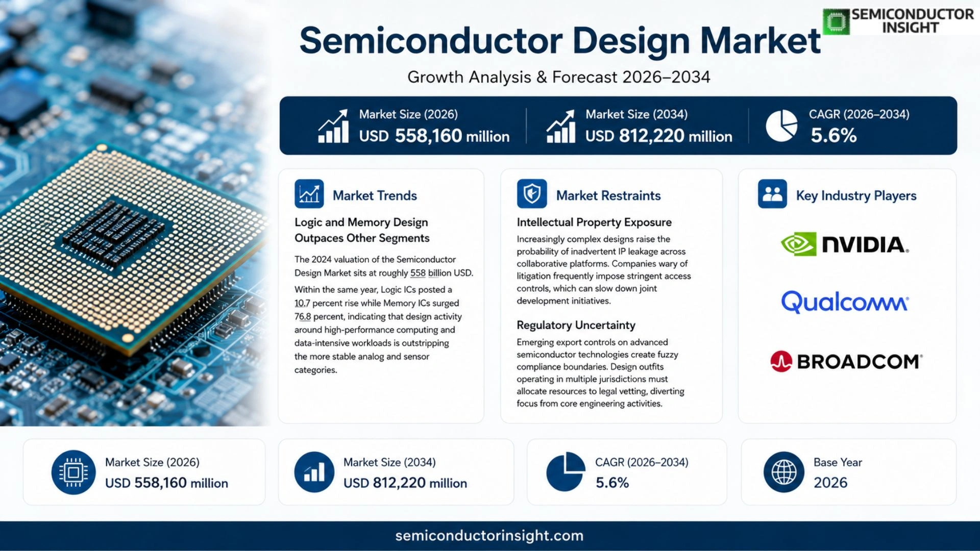
Semiconductor Design market size was valued at USD 558,160 million in 2026 and is projected to reach USD 812,220 million by 2034, exhibiting a CAGR of 5.6% during the forecast period.
Semiconductor design refers to the process of creating integrated circuits (ICs) using semiconductor materials such as silicon or gallium arsenide. The workflow typically includes circuit schematic capture, logical synthesis, physical layout and verification; electronic design automation (EDA) tools and advanced manufacturing processes are essential because they automate the transition from design intent to silicon fab production. IC design products underpin diverse applications,from consumer electronics like smartphones, tablets and wearables,to communications infrastructure and automotive systems.
The market expands as demand for high‑performance computing, AI accelerators and connected vehicles intensifies. WSTS’s Spring 2024 outlook lifted overall semiconductor growth to 16 %, driven by double‑digit gains in logic (10.7 %) and memory (76.8 %) segments. Growth is strongest in the Americas (+25.1 %) and Asia‑Pacific (+17.5 %). Leading firms,including NVIDIA, Qualcomm, Broadcom, AMD, MediaTek, Samsung and Intel,are accelerating investments in next‑generation IP blocks and advanced‑node collaborations, further stimulating design activity.
MARKET DRIVERS
Advanced Process Migration
The push toward sub‑10 nm lithography compels design houses to re‑engineer IP blocks, creating immediate demand for high‑precision design services. Companies that can shorten the verification loop are gaining a decisive edge, especially as volume shipments of next‑generation chips accelerate.
System‑Level Integration Trends
Customers are consolidating multiple functions,compute, memory, analog,into single die or package. This integration pressure forces designers to adopt heterogeneous architectures, which in turn fuels the need for specialized EDA workflows and cross‑domain expertise.
➤ “Design turnaround time is now the primary competitive lever for firms that serve the Semiconductor Design Market.”
In parallel, the rise of edge‑AI workloads is reshaping power‑budget constraints, prompting designers to embed ultra‑low‑power blocks early in the RTL stage. The ripple effect is a broader spend on simulation, power analysis, and custom IP development.
MARKET CHALLENGES
Escalating Tool Licensing Costs
Leading EDA vendors have shifted to subscription models with tiered pricing, driving up annual outlays for midsize design firms. When licensing fees consume a larger share of project budgets, companies must prioritize high‑margin contracts, limiting their ability to serve cost‑sensitive customers.
Other Challenges
Talent Shortage
The pool of engineers proficient in both advanced node design and AI‑assisted verification is thin. Recruitment cycles have lengthened, and attrition rates climb as specialists chase premium remuneration packages.
MARKET RESTRAINTS
Intellectual Property Exposure
Increasingly complex designs raise the probability of inadvertent IP leakage across collaborative platforms. Companies wary of litigation frequently impose stringent access controls, which can slow down joint development initiatives.
Regulatory Uncertainty
Emerging export controls on advanced semiconductor technologies create fuzzy compliance boundaries. Design outfits operating in multiple jurisdictions must allocate resources to legal vetting, diverting focus from core engineering activities.
MARKET OPPORTUNITIES
AI‑Enhanced Design Automation
Machine‑learning models that predict layout congestion and suggest optimal floor‑planning are moving from pilot projects to production tooling. Early adopters report a 15 % reduction in cycle time, positioning them to capture a larger share of the Semiconductor Design Market as customers seek faster time‑to‑market.
Open‑source silicon initiatives are lowering entry barriers for start‑ups, yet they simultaneously generate demand for professional verification services to assure reliability. Firms that can blend open frameworks with proprietary validation expertise stand to monetize a growing niche.
Semiconductor Design Market Trends
Logic and Memory Design Outpaces Other Segments
The 2024 valuation of the Semiconductor Design Market sits at roughly 558 billion USD. Within the same year, Logic ICs posted a 10.7 percent rise while Memory ICs surged 76.8 percent, indicating that design activity around high‑performance computing and data‑intensive workloads is outstripping the more stable analog and sensor categories. This divergence stems from escalating demand for artificial‑intelligence accelerators and high‑bandwidth memory in servers and edge devices. Companies that have ramped up advanced node support and integrated verification flows are seeing design cycles compress, which translates into faster time‑to‑market for flagship products. The competitive pressure forces designers to adopt more sophisticated electronic‑design‑automation (EDA) suites, thereby reshaping spending patterns toward tool licensing and custom IP development.
Other Trends
Regional Momentum Shifts
Geographically, the Americas posted a 25.1 percent year‑over‑year increase, while Asia‑Pacific recorded a 17.5 percent gain. Europe’s market barely moved, expanding only 0.5 percent, and Japan slipped by 1.1 percent. The disparity reflects divergent capital expenditure cycles: North American cloud providers are expanding data‑center footprints, and APAC manufacturers are scaling capacity to meet smartphone and automotive‑electronics demand. In contrast, European firms are contending with stricter regulatory constraints that temper investment in new design facilities. This regional split suggests that strategic partnerships and localized design services will become critical for firms seeking to capture growth in the two faster‑growing zones.
Emergence of Integrated EDA‑Chip Platforms
Beyond the hardware focus, the market is witnessing a consolidation of design and verification tools into unified platforms. Leading EDA vendors are bundling silicon‑prototyping, layout automation, and post‑silicon validation into end‑to‑end solutions, which reduces hand‑off friction between circuit architects and layout engineers. This trend is reinforced by the need to shorten design windows for complex nodes such as 3 nm and beyond. Firms that can embed these integrated platforms into their workflow gain a measurable advantage in design productivity, allowing them to allocate engineering resources toward differentiated architecture rather than routine layout tasks.
COMPETITIVE LANDSCAPE
Key Industry Players
Semiconductor Design Market – Competitive Overview
The design segment continues to be dominated by a handful of integrated circuit powerhouses that command both intellectual property breadth and deep relationships with foundries. NVIDIA’s GPU‑centric architecture platform remains a benchmark for high‑performance computing, while Intel leverages its legacy process expertise to sustain a diversified portfolio spanning data‑center, client, and edge applications. Samsung and MediaTek operate at the intersection of mobile and consumer silicon, translating massive wafer volumes into design leadership. The market structure reflects a tiered hierarchy: a few global innovators drive the most lucrative logic and memory design contracts, and a second tier of specialized firms focuses on analog, sensor, and automotive‑grade IP, creating a competitive environment that rewards both scale and niche expertise.
Beyond the headline names, a rich ecosystem of mid‑size and regionally focused players contributes essential building blocks. Companies such as Broadcom and Qualcomm continue to expand their system‑level offerings, integrating RF, connectivity, and security functions. European and Asian firms,including STMicroelectronics, Infineon, and NXP,excel in automotive and industrial ICs, where reliability standards shape design roadmaps. Meanwhile, memory‑centric entities like SK Hynix, Micron Technology, and Kioxia fuel the data‑intensive workloads that underpin AI accelerators. The presence of agile innovators such as Marvell and Realtek helps keep cost‑sensitive market segments competitive, ensuring that design innovation does not become confined to the largest fabs alone.
List of Key Semiconductor Design Companies Profiled
- NVIDIA
- Qualcomm
- Broadcom
- Advanced Micro Devices (AMD)
- MediaTek
- Samsung Electronics
- Intel
- SK Hynix
- Micron Technology
- Texas Instruments
- STMicroelectronics
- Kioxia
- Western Digital
- Infineon Technologies
- NXP Semiconductors
Segment Analysis:
| Segment Category | Sub-Segments | Key Insights |
| By Type |
|
Logic ICs
|
| By Application |
|
Mobile Devices
|
| By End User |
|
Consumer Electronics
|
| By Design Flow |
|
Verification & Validation
|
| By Technology Node |
|
Advanced Node
|
Regional Analysis: Semiconductor Design Market
North America
EDA providers are embedding machine‑learning kernels directly into schematic capture tools, enabling designers to explore layout permutations in near‑real time. This shift reduces manual iteration cycles and encourages more aggressive architecture experiments, especially in heterogeneous integration projects.
Universities in the corridor between Boston and Silicon Valley are tailoring curricula toward hardware‑software co‑design, ensuring a steady influx of engineers fluent in the latest verification languages and hardware description standards.
OEMs are favoring modular IP blocks with royalty‑free clauses to accelerate product diversification. This licensing flexibility is prompting design houses to adopt open‑source cores as foundational building blocks while retaining proprietary enhancements.
The latest node partnerships emphasize early design‑for‑manufacturability reviews, allowing silicon architects to align transistor layouts with process constraints before tape‑out, thereby mitigating costly re‑spins.
Europe
European design firms are capitalising on a regulatory environment that rewards energy efficiency. The EU’s Green Chip Initiative has nudged architects toward low‑power topologies, prompting a wave of research into near‑threshold voltage operation. Concurrently, cross‑border consortia are standardising interfaces for chiplet ecosystems, which eases integration across heterogeneous suppliers and accelerates time‑to‑revenue for niche market players. The region’s strong emphasis on standards compliance also means that design verification tools are evolving to meet stringent safety certifications, reinforcing Europe’s reputation for reliable, long‑lifecycle semiconductor solutions.
Asia‑Pacific
In Asia‑Pacific, the design landscape is shaped by rapid scaling of domestic foundries seeking to reduce reliance on external nodes. This self‑reliance drive fuels a collaborative model where design houses and fabs share design‑for‑manufacturability data streams, blurring traditional silos. At the same time, burgeoning consumer electronics demand is pushing companies to adopt modular design practices that enable swift product variants. The region’s investment in next‑generation packaging, such as fan‑out wafer‑level, adds another layer of design complexity, prompting a rise in specialised packaging‑aware design methodologies.
South America
South America remains a nascent yet opportunistic arena for semiconductor design. Governments are channeling grants toward hardware incubators that combine academia with start‑up ecosystems, fostering early‑stage innovations in IoT sensor design. While the market size is modest, the emphasis on low‑cost, high‑volume designs for agricultural and automotive telematics creates a distinct niche. Designers here are adopting open‑source toolchains to keep expenditures low, which also encourages community‑driven improvements and rapid knowledge transfer across borders.
Middle East & Africa
The Middle East & Africa region is leveraging its emerging data‑center investments to catalyse local design capabilities. Sovereign wealth funds are financing design studios that focus on security‑centric processors tailored for sovereign cloud initiatives. Parallelly, a growing number of universities are launching semiconductor labs, seeding a talent pool that can support regional fabless ambitions. Although the ecosystem is still embryonic, the strategic alignment of design activity with national digital transformation agendas is laying a foundation for future market participation.
Report Scope
This market research report provides a comprehensive analysis of the Semiconductor Design Market , covering the forecast period 2026–2034. It offers detailed insights into market dynamics, technological advancements, competitive landscape, and key trends shaping the industry.
Key focus areas of the report include:
- Market Overview: The report begins with an overview outlining its current market scenario, key growth indicators, and industry transformation drivers. It discusses macroeconomic factors, demand–supply balance, regulatory landscape, and the strategic role of semiconductors in powering advancements across industries such as automotive, telecommunications, consumer electronics, and industrial automation.
- Market Size & Forecast: Historical data and future projections for revenue, unit shipments, and market value across major regions and segments.
- Segmentation Analysis: Detailed breakdown by product type, technology, application, and end-user industry to identify high-growth segments and investment opportunities.
- Regional Insights: Insights into market performance across North America, Europe, Asia-Pacific, Latin America, and the Middle East & Africa, including country-level analysis where relevant.
- Competitive Landscape: Profiles of leading market participants, including their product offerings, R&D focus, manufacturing capacity, pricing strategies, and recent developments such as mergers, acquisitions, and partnerships.
- Technology Trends & Innovation: Assessment of emerging technologies, integration of AI/IoT, semiconductor design trends, fabrication techniques, and evolving industry standards.
- Market Drivers & Restraints: Evaluation of factors driving market growth along with challenges, supply chain constraints, regulatory issues, and market-entry barriers.
- Stakeholder Insights: Insights for component suppliers, OEMs, system integrators, investors, and policymakers regarding the evolving ecosystem and strategic opportunities.
Primary and secondary research methods are employed, including interviews with industry experts, data from verified sources, and real-time market intelligence to ensure the accuracy and reliability of the insights presented.
FREQUENTLY ASKED QUESTIONS:
What is the current market size of Semiconductor Design Market?
-> Semiconductor Design market size was valued at USD 558,160 million in 2026 and is projected to reach USD 812,220 million by 2034, exhibiting a CAGR of 5.6%
Which key companies operate in Semiconductor Design Market?
-> Key players include NVIDIA, Qualcomm, Broadcom, Advanced Micro Devices (AMD), MediaTek, Samsung, Intel, SK Hynix, Micron Technology, Texas Instruments, STMicroelectronics, Kioxia, Western Digital, Infineon, NXP, Analog Devices (ADI), Renesas, Microchip Technology, Onsemi, Sony Semiconductor Solutions, among others.
What are the key growth drivers?
-> Key growth drivers include rising demand for logic and memory ICs, expansion of mobile devices, automotive electronics, data‑center and AI workloads, and greater adoption of advanced EDA tools that accelerate design cycles.
Which region dominates the market?
-> The Americas remain the largest market by revenue, while Asia‑Pacific shows the highest growth rate, with projected increases of 25.1% and 17.5% respectively.
What are the emerging trends?
-> Emerging trends include integration of AI/IoT into semiconductor design, shift toward heterogeneous integration, and a focus on low‑power, high‑performance designs for edge computing and automotive applications.

Get Sample Report PDF for Exclusive Insights
Report Sample Includes
- Table of Contents
- List of Tables & Figures
- Charts, Research Methodology, and more...
 Download Sample Report PDF