
Key Statistics
Key Takeaways
- The market is rebased to USD 1,313.5 million in 2025 and USD 2,371.9 million in 2034, corresponding to a 6.8% CAGR during 2026–2034. The expansion is tied to rising deposition intensity per wafer as logic, memory and advanced packaging architectures add more conformal dielectric, barrier and spacer films.
- TEOS remains the largest type because it is entrenched in silicon-dioxide CVD and related dielectric processes, while HCDS is the strongest growth chemistry within the listed silicon-precursor set as low-temperature silicon nitride and conformal ALD/CVD requirements become more important in advanced structures.
- Semiconductor Chemical Vapor Deposition is the larger application base because it spans high-volume oxide, nitride and low-k film formation, while Atomic Layer Deposition is the faster-growing application as high-aspect-ratio features and atomic-scale thickness control increase the value of self-limiting deposition cycles.
- Asia Pacific is the largest regional market because the region concentrates the highest density of wafer-fabrication capacity and semiconductor materials consumption. North America and Europe are gaining strategic importance as public incentives pull more materials qualification, local technical support and supply-chain capacity closer to new fab clusters.
- Qualification rather than molecule availability is the principal commercial barrier. A precursor must deliver repeatable film composition, low metallic contamination, stable vapor delivery and acceptable by-products on the customer’s specific tool and process. That makes switching slower than in commodity chemicals and favors suppliers with application laboratories and local support.
- Competition is moving toward co-optimized material-and-delivery solutions. Suppliers increasingly compete on synthesis purity, container and delivery reliability, analytical capability, process-window knowledge and speed of customer qualification rather than on bulk chemical cost alone, raising the strategic value of regional R&D centers close to leading fabs.
Semiconductor ALD and CVD Silicon Precursors Market Overview
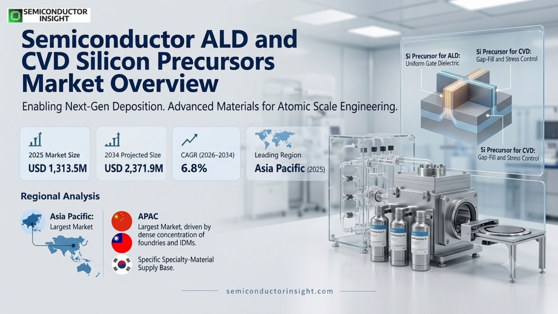
Semiconductor ALD and CVD Silicon Precursors Market is valued at USD 1,313.5 million in 2025 and is projected to reach USD 2,371.9 million by 2034, expanding at a 6.8% CAGR during 2026–2034. Asia Pacific is the largest market in 2025 because it combines the world’s deepest concentration of foundry, memory and integrated-device manufacturing with a dense specialty-materials supply base.
Semiconductor ALD and CVD silicon precursors are ultra-high-purity silicon-containing chemicals engineered to form silicon oxide, silicon nitride, silicon carbide and related thin films during wafer fabrication. The defined market includes TEOS, HCDS, 3MS, 4MS and other silicon precursor chemistries sold into atomic layer deposition and chemical vapor deposition processes. Value is created not merely by supplying a molecule, but by delivering a stable chemistry with contamination control, qualified packaging and repeatable vapor transport at production scale.
The commercial scope is tightly linked to deposition intensity rather than semiconductor unit shipments alone. Advanced logic uses more spacer, liner, dielectric and barrier steps; 3D NAND repeats film stacks through very high aspect-ratio structures; DRAM scaling increases materials complexity; and heterogeneous integration adds deposition steps beyond the front end. A wafer therefore can consume more qualified precursor value even when wafer starts grow modestly, which is why process complexity is a central demand mechanism for this market.
Material specifications are unusually demanding because trace contaminants can create defects across thousands of dies on a wafer. Supplier capability therefore extends from synthesis and purification through analytical metrology, cylinder or ampoule preparation, shelf-life control, delivery compatibility and process support. Entegris, for example, markets TEOS for CVD, HCDS for CVD and ALD silicon-nitride processes, and 4MS for low-k dielectric deposition, illustrating how individual silicon chemistries map to different film functions and tool conditions.
The market is changing now because fab investment and materials intensity are rising together. SEMI reported that global semiconductor materials revenue reached USD 73.2 billion in 2025, while wafer-fabrication materials grew to USD 45.8 billion. The same industry cycle is also supporting record equipment investment. For precursor suppliers, the commercial implication is a larger qualification pipeline, but also higher expectations for regional availability, sustainability, contamination control and customer-specific process engineering.
Segment Analysis: By Type
By type, the market is segmented into TEOS, HCDS, 3MS, 4MS and Others. TEOS is the largest established segment because of its broad use in oxide deposition, while HCDS has the strongest growth profile within the listed chemistries as manufacturers seek low-temperature, conformal silicon-nitride films for increasingly complex logic and memory structures.
| Type | Technical role | Market position |
|---|---|---|
| TEOS | Tetraethyl orthosilicate is a liquid silicon source used extensively in CVD oxide processes. Its commercial strength comes from a long qualification history, stable handling characteristics and broad compatibility across dielectric-film applications. The segment is mature but structurally durable because oxide films remain fundamental to isolation, interlayer dielectrics and process integration across both mature and advanced semiconductor nodes. | Largest listed type. Purchasing emphasizes consistent assay, very low metallic contamination, predictable water control and secure bulk or container logistics. Because TEOS is used across many fabs and generations, suppliers compete on high-volume reliability and customer-approved purity rather than on novelty alone; qualification history and installed delivery infrastructure make incumbent positions difficult to displace. |
| HCDS | Hexachlorodisilane serves CVD, ALD and related low-temperature silicon-nitride deposition routes. Its value rises when device structures require conformal nitride films at temperatures compatible with sensitive underlying layers. As gate-all-around structures, advanced memory stacks and tighter thermal budgets increase process complexity, HCDS gains relevance where conventional silicon sources cannot provide the same combination of film quality and deposition conditions. | Strongest growth profile among the named types. The opportunity is concentrated in advanced process modules where low-temperature film performance and precursor purity justify a premium. Commercial success depends on controlling chlorine-related impurities and by-products, maintaining stable delivery, and supporting tool-specific process windows. Qualification can be lengthy, so suppliers with local applications teams have an advantage. |
| 3MS | Trimethylsilane is used in silicon-carbon and low-k dielectric film schemes where the precursor’s carbon-containing structure contributes to the targeted film composition. Demand is more application-specific than TEOS and is linked to interconnect dielectric engineering, plasma-enhanced CVD conditions and device architectures that need controlled dielectric constant, mechanical strength and integration compatibility across backend-of-line process flows. | Specialty segment with defensible value where the chemistry is embedded in a qualified dielectric recipe. Its growth is governed less by overall wafer starts and more by adoption of specific low-k, silicon-carbon or barrier schemes. Supplier differentiation centers on impurity control, batch consistency and delivery behavior because even small variations can change plasma chemistry and final film properties. |
| 4MS | Tetramethylsilane is a volatile organosilicon precursor used in chemical vapor deposition of carbon-containing dielectric films and related silicon-carbon-nitrogen layers. Its low boiling point makes delivery-system design and process control important. Demand is connected to interconnect engineering and specialized film stacks rather than to every wafer, which keeps the addressable base narrower than TEOS while preserving higher technical differentiation. | A targeted specialty chemistry rather than a broad-volume oxide source. Suppliers compete on extremely high purity, stable canister handling, vapor-delivery consistency and compatibility with customer plasma conditions. The segment benefits when device interconnects require low-k or silicon-carbon-based films, but its commercial exposure is sensitive to process-recipe changes because customers can redesign dielectric stacks over successive technology generations. |
| Others | The remaining category covers additional silicon-bearing ALD and CVD precursors selected for specific reactivity, thermal window, film composition or surface-chemistry requirements. It includes chemistries developed for emerging silicon oxide, nitride, carbide and mixed films where standard molecules do not deliver sufficient conformality, low-temperature performance or impurity control. New formulations usually begin in research quantities before moving through tool and fab qualification. | Innovation-led segment with the highest formulation diversity. Revenue is fragmented across smaller-volume chemistries, but successful materials can command strong value once qualified in an advanced process. Development risk is high because many candidates never reach high-volume manufacturing; suppliers therefore prioritize close collaboration with device makers and equipment companies to screen chemistries against realistic process windows before scaling synthesis. |
Commercial positioning by precursor chemistry
Pricing power generally increases with technical specificity, purification burden and qualification depth. High-volume TEOS is purchased with strong attention to delivered cost and supply assurance, while advanced HCDS and emerging precursor formulations can sustain a greater technical premium when they solve a temperature, conformality or defect problem that materially affects yield. The most defensible margins therefore sit where a supplier combines proprietary chemistry, purification know-how, qualified packaging and application support rather than selling an interchangeable bulk molecule.
Segment Analysis: By Application
By application, the market is segmented into Semiconductor Atomic Layer Deposition and Semiconductor Chemical Vapor Deposition. Chemical Vapor Deposition represents the larger installed consumption base, while Atomic Layer Deposition is the faster-growing application because advanced device geometries increasingly require conformal films and atomic-scale thickness control on three-dimensional structures. The requirement is strongest in advanced logic and memory structures where uniform deposition through high-aspect-ratio features directly affects process yield and electrical performance.
| Application | Demand characteristics |
|---|---|
| Semiconductor Atomic Layer Deposition | ALD consumes precursor in sequential, self-limiting surface reactions that can deliver highly conformal films over deep and complex features. The purchasing trigger is not simply new fab capacity; it is the addition of device structures where conventional line-of-sight or faster CVD processes cannot meet thickness uniformity and interface requirements. Growth is strongest in advanced logic, DRAM, 3D NAND and specialized films with tight thermal budgets. |
| Semiconductor Chemical Vapor Deposition | CVD remains the larger consumption base because it is established across oxide, nitride, low-k and other dielectric-film steps throughout front-end and interconnect manufacturing. Customers prioritize throughput, repeatability, precursor utilization and stable film properties across long production runs. Demand therefore scales with both wafer starts and the number of qualified deposition layers per wafer, preserving a broad market even as ALD expands in selected advanced modules. |
Secondary Segmentation: By End User
| End User | Purchasing logic and market role |
|---|---|
| Foundries | Foundries form the largest end-user group because they operate high-volume multi-customer fabs and must qualify deposition materials across multiple technology platforms. Their procurement decisions weigh yield stability, supply continuity, second-source strategy and global technical support. A precursor that wins a foundry process of record can scale rapidly across multiple customer designs, but qualification standards are stringent and change control is tightly governed. |
| IDMs (Integrated Device Manufacturers) | IDMs combine device design and manufacturing, allowing precursor selection to be co-optimized with proprietary process architecture. Memory and analog IDMs can generate large, recurring consumption when a chemistry is embedded across several layers or generations. Supplier relationships are typically long term because process recipes, contamination specifications and material-delivery systems are interconnected, making technical support and roadmap alignment more important than spot pricing. |
| Research Institutes | Research institutes and pilot lines purchase smaller volumes but play an outsized role in early material screening. They evaluate new precursor families, film properties and process windows before commercial device makers commit to high-volume qualification. This segment therefore acts as an innovation gateway: revenue is limited at the research stage, but successful demonstrations can create later commercial opportunities with equipment vendors, foundries and IDMs. |
Regional Analysis
Asia Pacific leads the market because Taiwan, South Korea, China and Japan combine dense wafer-fabrication capacity with major materials suppliers and application laboratories. North America is becoming more strategically important as fab clusters and supply-chain incentives pull chemical capability closer to domestic manufacturing, while Europe emphasizes specialty semiconductor ecosystems, resilience and lower-impact materials. South America and Middle East & Africa remain smaller, investment-led opportunities.
How does regional demand differ across the semiconductor silicon-precursor market?
Regional demand is determined by more than semiconductor revenue. Silicon precursors must be qualified on specific deposition tools and device flows, so proximity to fabs, analytical laboratories and technical service matters materially. Asia Pacific combines the largest production base with short feedback loops between chipmakers and materials suppliers. North America and Europe are using industrial policy to deepen local supply chains. Emerging regions are building design, research and selective manufacturing capabilities first, which creates smaller but strategically important precursor opportunities.
| Region | Position | Growth outlook | Demand profile | What decides supplier selection |
|---|---|---|---|---|
| Asia Pacific | Largest | Highest absolute demand | Foundry, memory and materials cluster | Supplier selection is strongly influenced by demonstrated fab qualification, rapid local technical response and secure high-purity logistics. The region’s dense manufacturing footprint rewards suppliers that can synthesize or package close to customers, maintain dual-site continuity and support process tuning on short development cycles. Price matters, but contamination performance and continuity are decisive once a chemistry enters a production recipe. |
| North America | Major high-value market | Strong localization momentum | Advanced logic, memory, R&D and new fab clusters | Customers increasingly value domestic or regionally resilient supply alongside advanced applications support. New fab clusters create opportunities for local analytical laboratories, canister management and materials manufacturing, while established R&D centers require suppliers to collaborate early on next-generation deposition. Qualification remains global, so a North American footprint is most valuable when it complements a supplier’s existing Asian and European production network. |
| Europe | Specialty and resilience market | Steady expansion | Automotive, power, industrial and research-led semiconductor base | European buyers place substantial weight on chemical stewardship, traceability, energy and emissions performance, as well as technical fit for automotive, power and specialty semiconductor processes. The region’s industrial policy supports new capacity, but the supplier opportunity is concentrated in qualified materials and local technical support rather than commodity volume. Companies with strong regulatory systems and specialty-chemistry capability are well positioned. |
| South America | Emerging | Early-stage growth | Policy-led ecosystem development centered on Brazil | The market is still developing and procurement is more dependent on imported material, distributor capability and the pace at which local semiconductor programs move from policy to production. Suppliers must manage longer logistics chains and smaller order sizes while preserving semiconductor-grade handling. The strongest near-term opportunity is to support pilot, research and specialty manufacturing programs rather than build large dedicated precursor capacity prematurely. |
| Middle East & Africa | Emerging | Selective strategic growth | Design, research and targeted manufacturing initiatives | Commercial access depends on whether national semiconductor initiatives progress from design and research toward wafer fabrication or materials pilot activity. Suppliers can enter through universities, technology centers and multinational customers before high-volume fabs exist. Reliable import handling, training and technical service are essential because local ultra-high-purity chemical infrastructure is less developed than in the major Asian semiconductor clusters. |
Semiconductor ALD and CVD Silicon Precursors Manufacturers and Competitive Landscape
Competition is defined by a small group of global advanced-materials suppliers and a wider set of regional specialty-chemical companies. Winning positions depend on ultra-high-purity synthesis, analytical control, qualified delivery hardware, regional technical support and the ability to co-develop chemistries with device makers. Once a precursor is embedded in a production recipe, qualification and change-control requirements create meaningful customer stickiness.
Large multinational suppliers compete through portfolio breadth and global service. Merck Group, Air Liquide, Entegris and DuPont can combine specialty chemistry with extensive analytical, logistics or process-support infrastructure. This matters when a customer wants common quality systems across several fabs or needs integrated delivery and contamination-control expertise. Their scale, however, does not remove the need for molecule-specific performance; each precursor must still win qualification on film quality, defectivity and cost of ownership.
Asian specialty suppliers compete on proximity to the world’s largest wafer-fabrication clusters. SK Materials, SoulBrain, DNF Solutions, Mecaro and other regional companies can support rapid customer interaction and may have strong positions in Korean memory and foundry ecosystems. UP Chemical and Chinese suppliers add further competitive pressure. Locality is valuable because a process excursion can require immediate analytical work, replacement material and joint troubleshooting, making response time a commercial differentiator.
R&D capability is becoming more visible in supplier strategy. Entegris opened a Korea Technology Center with advanced deposition-materials application support, while ADEKA launched a major semiconductor innovation center with multiple ALD systems. These investments show that suppliers increasingly need to reproduce customer-relevant process conditions before a material reaches a fab. The ability to generate film data, analyze impurities and iterate molecular design can reduce qualification risk and defend pricing.
The competitive boundary also includes delivery technology and packaging. A chemically pure material can still fail commercially if the container, valve, vapor-delivery profile or refill process introduces contamination or instability. Suppliers that control chemistry and delivery as one system can therefore offer a stronger process guarantee. This favors companies with semiconductor-specific canister management, filtration and lifecycle support, while smaller suppliers often differentiate through a narrower chemistry portfolio and customer-specific development.
Tier structure
| Competitive tier | Companies | Competitive position |
|---|---|---|
| Global integrated materials leaders | Merck Group; Air Liquide; Entegris; DuPont | These companies combine international customer coverage with advanced analytical systems, high-purity manufacturing and broad semiconductor-materials portfolios. Their advantage is strongest when customers need consistent quality across multiple regions, technical support through qualification and resilient logistics. They compete on total process assurance rather than the molecule alone, which can support long-term relationships with leading foundries and IDMs. |
| Asia-based precursor specialists | SK Materials; SoulBrain Co Ltd; ADEKA; DNF Solutions; Mecaro; UP Chemical (Yoke Technology) | These suppliers benefit from proximity to Korean, Japanese, Taiwanese and broader Asian wafer-fab clusters. Their competitive position is built on customer intimacy, specialized deposition chemistry and rapid technical response. Several also invest directly in ALD evaluation and local R&D, allowing them to compete for advanced-node qualifications where process knowledge and contamination performance matter more than global brand scale. |
| Regional and emerging specialists | Botai Electronic Material; Natachem and other specialty suppliers | Smaller suppliers target selected chemistries, domestic localization programs or customer-specific applications. They can compete effectively where a customer seeks a second source or where a local supplier can reduce logistics risk. The principal hurdle is proving batch-to-batch consistency and supporting qualification at the same technical depth as established global competitors, particularly for advanced processes with extremely tight impurity limits. |
Key companies profiled
- SK Materials
- UP Chemical (Yoke Technology)
- Merck Group
- Air Liquide
- Entegris
- SoulBrain Co Ltd
- ADEKA
- DNF Solutions
- Mecaro
- Botai Electronic Material
- Natachem
- DuPont
Semiconductor ALD and CVD Silicon Precursors Production Capacity Analysis
Production capacity is constrained less by reactor volume than by the ability to manufacture, purify, analyze, package and release semiconductor-grade material repeatedly. A precursor plant must maintain tight control of metallic and moisture contamination, while qualified containers and delivery systems must preserve that purity to the point of use. The practical capacity of a supplier is therefore the amount of customer-qualified material it can ship consistently, not the nominal chemical output of a synthesis line.
Upstream synthesis begins with high-purity silicon-bearing feedstocks and organic or halogenated reagents, followed by reaction, separation and purification. Distillation, filtration and analytical release can be more important to usable output than gross synthesis yield because semiconductor customers specify contaminants at trace levels. Equipment is commonly dedicated or tightly segregated to prevent cross-contamination. Capacity expansion therefore requires investment in analytical instruments, clean handling areas and trained operators alongside reactors and storage.
Qualification creates another capacity constraint. A new production line or even a change in raw-material source can require customer review because the chemistry is part of a sensitive wafer process. Suppliers must preserve lot genealogy, analytical methods and change-control procedures while ramping. This slows the conversion of newly installed physical capacity into revenue-bearing capacity. It also explains why customers often qualify more than one manufacturing site for strategically important materials even when one plant could satisfy the volume.
Geographically, Asia Pacific holds the deepest combination of precursor production and customer demand, particularly in South Korea, Japan, Taiwan and China. North American and European expansion is increasingly focused on resilience, R&D and support around new fab clusters. The most efficient network is therefore not a single global mega-plant but a qualified multi-site system that separates core synthesis from regional packaging, inventory, analytical response and customer support where appropriate.
Capacity strategy must also account for molecule volatility and storage behavior. TEOS can be handled as a stable high-volume liquid, while other precursors may need tighter temperature, pressure or container controls. Specialized materials can have lower annual tonnage but higher value per kilogram and more intensive analytical requirements. Suppliers that treat every chemistry as the same manufacturing problem risk either overbuilding low-volume assets or underinvesting in the controls needed for advanced qualifications.
Semiconductor ALD and CVD Silicon Precursors Market Dynamics: Drivers, Restraints and Opportunities
Market growth is driven by greater deposition intensity per wafer, sustained investment in logic and memory capacity, and the need for conformal low-temperature films in three-dimensional device architectures. Restraints include long material qualification cycles, high purification and analytical costs, environmental and safety obligations, and customer concentration. Opportunities are strongest in next-generation low-temperature chemistries, regionalized supply and co-development with equipment makers and leading fabs.
Market Drivers
MARKET DRIVERS
Drivers Impact Analysis*
| Factor | Directional impact | Geographic relevance | Impact timeline |
|---|---|---|---|
| Rising deposition intensity per wafer Advanced logic, DRAM and 3D NAND add more film interfaces, liners, spacers and high-aspect-ratio structures, increasing the number and technical difficulty of deposition steps. This expands precursor value even without one-for-one growth in wafer starts. Suppliers benefit when a new architecture requires a chemistry with better conformality, lower thermal budget or tighter impurity control than the prior generation. |
High | Global; strongest in advanced Asian and U.S. fabs | Long term |
| Record semiconductor manufacturing investment SEMI reported record semiconductor equipment billings in 2025 and continued strong investment tied to advanced logic and memory. Each new or expanded wafer-fab module creates qualification opportunities for deposition materials, delivery systems and local technical support. The effect on precursor demand is strongest after tools enter process qualification and production, so materials revenue follows fab construction with a meaningful ramp period. |
High | Asia Pacific, North America, Europe | Medium to long term |
| Localization of semiconductor material supply Government programs increasingly support not only fabs but also chemicals, gases, materials and equipment. Customers are responding by asking suppliers for regional inventories, second-source plans and local analytical capability. This does not necessarily duplicate every synthesis step in each region, but it raises the commercial value of multi-site qualification, local packaging and technical centers that reduce disruption risk. |
Medium | North America and Europe; also China | Medium term |
| Expansion of ALD in complex device structures Atomic layer deposition becomes more valuable when surfaces are three-dimensional and thickness control must remain uniform through deep features. Gate-all-around logic, advanced memory capacitors and high-layer-count NAND create more such conditions. Silicon precursor suppliers can capture this growth by developing molecules with suitable reactivity, volatility and thermal windows while minimizing residues and corrosive by-products. |
High | Advanced logic and memory clusters | Long term |
*Directional assessment indicates relative commercial influence within this market and is not a measured contribution to the headline CAGR.
Higher film complexity increases materials value per wafer
Semiconductor scaling no longer depends only on shrinking lateral dimensions. Device makers increasingly add three-dimensional structures, new interfaces and more complicated material stacks, which increases the number of deposition steps and the difficulty of each step. This changes the demand equation for precursors: market value can rise through greater process intensity even if wafer-start growth is moderate. Suppliers with chemistries designed for conformality, low-temperature operation and cleaner film interfaces therefore gain exposure to technology migration itself.
Fab investment broadens the qualification pipeline
A new fab does not immediately translate into full precursor consumption because each material must pass equipment and device qualification, but it expands the future pipeline of production opportunities. SEMI’s 2025 equipment data shows a manufacturing cycle led by advanced logic and memory investment. For precursor suppliers, the commercial task is to engage before high-volume production, secure test capacity and provide repeatable material lots through process development so that the chemistry is included in the eventual production recipe.
Supply-chain resilience creates local service and manufacturing demand
Semiconductor customers increasingly evaluate whether a materials supplier can recover from geopolitical, transport or plant disruptions without forcing a process change. That shifts procurement toward qualified second sites, regional inventory and transparent raw-material sourcing. U.S. CHIPS funding explicitly includes semiconductor chemicals and gases, while Europe’s policy framework emphasizes ecosystem resilience. The market implication is more capital directed toward regional analytical, packaging and support capability even when the core molecule is already available globally.
ALD expands where conformality and thermal budget dominate
ALD’s self-limiting surface chemistry is particularly useful when device geometry prevents conventional deposition from maintaining uniform thickness or when a narrow thermal window is required. The technique is therefore gaining strategic importance in advanced logic and memory. Silicon precursors that provide predictable nucleation, low impurities and clean reaction by-products can win premium applications. The growth path favors suppliers able to test films on representative ALD tools rather than offering chemistry without process-level evidence.
Market Restraints
MARKET RESTRAINTS
Restraints Impact Analysis*
| Factor | Directional impact | Geographic relevance | Impact timeline |
|---|---|---|---|
| Long customer qualification and change control A precursor change can alter film composition, defectivity, chamber condition and device yield, so customers require extensive qualification before production use. Once qualified, any manufacturing-site, raw-material or packaging change can trigger further review. This slows adoption of new suppliers and delays revenue from newly installed capacity, favoring incumbents but also making the market less responsive to short-term price competition. |
High | Global | Persistent |
| Ultra-high-purity manufacturing cost Semiconductor-grade materials require purification, trace-metal analysis, controlled packaging and clean handling far beyond ordinary industrial chemical practice. These capabilities add fixed cost and limit the number of credible suppliers. As process nodes become more sensitive to contamination, analytical detection limits and release testing become more demanding, potentially increasing cost even when raw-material prices are stable. |
Medium to High | Global | Persistent |
| Environmental, safety and by-product constraints Chlorinated and volatile precursor systems require rigorous occupational, transport and emissions controls. Customers also evaluate process gases and by-products as part of facility sustainability programs. A chemistry that performs well electrically can therefore lose attractiveness if it creates difficult abatement, corrosive residues or high lifecycle burden. Suppliers must invest in safer formulations, packaging and process-efficiency improvements. |
Medium | North America and Europe especially | Medium to long term |
| Customer and regional concentration A large share of global advanced wafer fabrication is concentrated among a limited number of foundries and memory manufacturers in Asia. This creates large opportunities but also significant account risk because a lost qualification can remove a substantial revenue stream. Suppliers must balance deep customer integration with portfolio diversification across regions, device types and precursor families. |
Medium | Asia Pacific concentrated | Persistent |
*Directional assessment indicates relative commercial influence within this market and is not a measured contribution to the headline CAGR.
Qualification timelines slow supplier switching
A low-priced precursor is not attractive if adopting it requires months of process testing and exposes a fab to yield risk. Device makers therefore switch material suppliers cautiously, especially for advanced nodes. This protects established positions but raises the cost of customer acquisition for challengers. New suppliers must usually demonstrate equivalent film properties, contamination performance, delivery stability and lot consistency over repeated trials before commercial volume is considered, which stretches the time between R&D expenditure and revenue.
Purity and analytics create high fixed costs
The cost base is shaped by what must be removed and measured rather than by the bulk molecule alone. Metallic contaminants, water and particles can be unacceptable at levels irrelevant to conventional chemical markets. Producers need dedicated purification, clean filling, semiconductor-compatible containers and sophisticated analytical methods. These fixed capabilities are difficult to justify for small-volume chemistries, which can slow the scale-up of novel precursors until a customer qualification provides enough committed demand.
Safety and sustainability requirements can narrow the usable chemistry set
Precursor selection must account for transport classification, worker exposure, flammability, corrosivity, chamber by-products and abatement load. Environmental requirements can therefore change the commercial attractiveness of otherwise effective molecules. Customers increasingly prefer materials that deliver the required film at lower process temperature or with fewer problematic by-products. Suppliers unable to redesign chemistry or delivery can face gradual displacement even when legacy processes remain technically functional.
Dependence on a small number of leading fabs raises account risk
Advanced precursor consumption is concentrated in fabs with the technology and capital to run leading logic and memory processes. A supplier can scale quickly after winning one major customer, but the reverse is also true: a recipe change, node transition or loss of preferred-supplier status can materially reduce demand. Building a resilient portfolio therefore requires multiple device platforms, geographies and chemistries rather than relying on a single high-volume qualification.
Market Opportunities
MARKET OPPORTUNITIES
Low-temperature and high-conformality silicon chemistries
The most attractive formulation opportunity is to solve process windows where incumbent silicon sources are too hot, too slow or insufficiently conformal. Gate-all-around structures, advanced memory features and sensitive integration sequences reward precursors that provide strong surface reactivity without unwanted gas-phase decomposition. Suppliers that can demonstrate film density, impurity control and clean by-products on realistic tools can capture premium qualifications and build long-lived positions around proprietary chemistry.
Regional qualification and second-source programs
Customers are expanding supplier-risk reviews beyond price and quality to include geographic concentration and recovery time. This creates opportunities for established suppliers to qualify second production sites and for regional specialists to enter as alternative sources. The winning model is not simple duplication: the second site must reproduce impurity fingerprints, packaging, analytical release and process performance closely enough that customers can switch supply without changing the wafer recipe.
Materials-and-delivery co-optimization
Precursor performance depends on storage, vaporization, line temperature, flow stability and chamber delivery as well as molecular chemistry. Suppliers that integrate material design with canisters, valves, filtration and delivery engineering can solve a wider part of the customer’s problem and reduce process variability. This creates additional value capture and can strengthen customer lock-in, particularly for less volatile or temperature-sensitive materials used in advanced ALD and CVD.
Advanced packaging and heterogeneous integration
As advanced packaging adds redistribution, dielectric, barrier and bonding-related process steps, deposition materials gain new demand outside traditional front-end transistor fabrication. Not every package flow uses the same silicon precursors, but suppliers with ALD/CVD expertise can extend into adjacent films and process modules. The opportunity is strongest for companies that coordinate front-end chemistry knowledge with packaging R&D so they can follow customers as more integration moves into three-dimensional package structures.
Semiconductor ALD and CVD Silicon Precursors Supply Chain Analysis
The value chain runs from high-purity silicon and organic or halogenated feedstocks through precursor synthesis, purification and analytical release, then into semiconductor-specific containers and delivery systems before reaching fab deposition tools. The highest value is created where chemistry and contamination control meet customer qualification. Bottlenecks arise from qualified raw materials, specialized purification, clean packaging, analytical capacity and the time required to approve any change in the chain.
Upstream value is concentrated in feedstocks that can meet semiconductor purity and consistency requirements. A nominally identical industrial reagent may be unsuitable if trace metals, water or lot variability exceed the precursor producer’s purification capability. Suppliers therefore qualify raw-material sources carefully and may maintain multiple approved sources for continuity. When upstream changes occur, analytical equivalence must be established before material is introduced into the precursor synthesis process.
The precursor producer captures the greatest specialized value through molecular design, purification, analytical release and intellectual property around manufacturing conditions. Synthesis scale alone is not sufficient; the supplier must repeatedly deliver a material whose impurity profile and physical behavior remain inside a narrow process window. This is where experienced semiconductor chemical companies differentiate from general industrial-chemical producers and where new entrants face the steepest technical learning curve.
Packaging and logistics form an extension of product quality. Moisture ingress, particle generation, valve contamination or inconsistent heel volume can undermine a high-purity molecule before it reaches the tool. Semiconductor suppliers therefore qualify containers and cleaning procedures alongside chemistry. Regional inventory reduces transport risk but also requires disciplined shelf-life management and container return systems, especially for materials shipped in reusable high-value canisters.
At the fab, material qualification closes the value chain. Device makers evaluate film thickness, composition, electrical properties, defectivity, chamber behavior and downstream integration before approving a source. Once in production, statistical process control and change management govern continued use. The commercial implication is that supplier relationships extend well beyond the purchase order: applications engineers, analytical laboratories and logistics teams all contribute to the customer’s cost of ownership and willingness to maintain a qualification.
Recent Developments in the Semiconductor ALD and CVD Silicon Precursors Market
- 02 Jul 2026
ADEKA announced full-scale operation of its Semiconductor Innovation Center in Saitama, featuring an over 850 m² cleanroom, multiple ALD systems and expanded work on high-k and next-generation deposition materials. The facility strengthens the company’s ability to evaluate precursor chemistry under semiconductor-relevant conditions and coordinate development with bases in South Korea, Taiwan and the United States, increasing competitive pressure on suppliers without comparable application infrastructure. Source - 14 Apr 2026
Air Liquide described new local production serving semiconductor growth in Asia, including three new plants opened in South Korea during the prior 18 months to secure critical molecules for chipmakers. The development reinforces the importance of regional ultra-high-purity supply and long-term customer contracts. For precursor markets, local production lowers logistics exposure and improves response time when customers change process demand or require rapid technical support. Source - 21 Aug 2025
Entegris announced a USD 700 million U.S. R&D investment program and an Illinois technology center covering deposition materials and other semiconductor process solutions. The move expands domestic applications capability close to new U.S. fab clusters. It shows how precursor suppliers are allocating capital toward customer co-development and technical infrastructure, not only bulk synthesis, as qualification speed and process integration become more important competitive factors. Source - 18 Jul 2025
Entegris opened its Korea Technology Center in Ansan with R&D, analytical and application support for advanced deposition materials. The center provides closer technical engagement with Korean chipmakers and supports process demonstration in cleanroom conditions. This type of regional applications investment can shorten troubleshooting and qualification cycles, which is particularly important for new silicon precursors where film performance depends on the interaction between chemistry, delivery and tool conditions. Source - 12 May 2026
SEMI reported that global semiconductor materials revenue reached USD 73.2 billion in 2025, including USD 45.8 billion of wafer-fabrication materials. The growth was associated with higher process complexity, advanced nodes, high-performance computing and high-bandwidth memory. These drivers directly support the commercial environment for ALD and CVD precursors because more complex devices require additional and more demanding thin-film deposition steps. Source
REPORT SCOPE & SEGMENTATION
| Attribute | Details |
|---|---|
| Study Period | 2020–2034 |
| Base Year | 2025 |
| Estimated Year | 2026 |
| Forecast Period | 2026–2034 |
| 2025 Market Size | USD 1,313.5 million |
| 2026 Estimated Size | USD 1,402.6 million |
| 2034 Projected Market Size | USD 2,371.9 million |
| CAGR | 6.8% during 2026–2034 |
| Largest Market in 2025 | Asia Pacific |
| By Type | TEOS; HCDS; 3MS; 4MS; Others |
| By Application | Semiconductor Atomic Layer Deposition; Semiconductor Chemical Vapor Deposition |
| By End User | Foundries; IDMs (Integrated Device Manufacturers); Research Institutes |
| Regions | North America; Europe; Asia-Pacific; South America; Middle East & Africa |
| Companies Profiled | SK Materials; UP Chemical (Yoke Technology); Merck Group; Air Liquide; Entegris; SoulBrain Co Ltd; ADEKA; DNF Solutions; Mecaro; Botai Electronic Material; Natachem; DuPont |
Frequently Asked Questions
What is the current size of the semiconductor ALD and CVD silicon precursors market?
The global market is valued at USD 1,313.5 million in 2025 and is projected to reach USD 2,371.9 million by 2034, representing a 6.8% CAGR during 2026–2034. Growth reflects rising thin-film deposition intensity across advanced logic, DRAM, 3D NAND and adjacent semiconductor processes, where tighter geometry and three-dimensional structures increase the need for highly controlled silicon oxide, nitride and related films.
Which precursor type is the largest segment?
TEOS is the largest listed type because it has a broad and long-established role in silicon-dioxide deposition across semiconductor manufacturing. Its installed process base spans many device generations, making demand less dependent on a single advanced-node transition. Suppliers still compete intensely on purity, moisture control, lot consistency, container cleanliness and logistics because any variation can affect film properties and fab yield.
Which precursor type has the strongest growth profile?
HCDS has the strongest growth profile within the listed chemistries because it can support silicon-nitride deposition through CVD, ALD and related low-temperature processes. More complex logic and memory architectures increase the value of conformal nitride films formed under tighter thermal constraints. Commercial growth therefore depends on winning advanced process qualifications rather than replacing TEOS across its much broader oxide-deposition base.
Which deposition application is growing fastest?
Semiconductor Atomic Layer Deposition is the faster-growing application because its self-limiting surface reactions provide conformality and atomic-scale thickness control on complex three-dimensional features. Advanced logic structures, DRAM capacitors and high-layer-count memory create more use cases where conventional deposition cannot maintain the required uniformity. Chemical Vapor Deposition remains the larger installed consumption base because it serves a wider range of established high-volume films.
Why is Asia Pacific the largest regional market?
Asia Pacific is the largest region because it concentrates the majority of global semiconductor manufacturing investment and includes the major foundry, memory and materials ecosystems of Taiwan, South Korea, China and Japan. The region also hosts extensive local precursor synthesis, packaging, analytical and applications capability. That density shortens customer qualification cycles and creates recurring consumption close to high-volume wafer fabs.
What determines supplier selection in this market?
Supplier selection is driven by film performance, impurity control, delivery stability, lot-to-lot consistency, change management and the ability to support qualification on the customer’s specific tool and process. Price is relevant but rarely decisive by itself because a material-related yield excursion is far more costly than a small chemical-price difference. Fabs therefore favor suppliers that combine reliable manufacturing with responsive analytical and applications support.
Why are precursor qualification cycles long?
A new precursor source can change film composition, nucleation behavior, chamber condition, by-products, particle performance and downstream device yield. Customers must therefore test repeated lots across relevant process conditions before approving production use. Changes to manufacturing site, raw materials, packaging or analytical methods can also require review. This rigorous change-control system protects yield but delays market entry for new suppliers and newly installed capacity.
How does regional supply-chain localization affect the market?
Localization increases the value of qualified second manufacturing sites, regional inventory, local analytical laboratories and applications teams. Government programs in the United States and Europe are also supporting semiconductor materials and supply-chain infrastructure. Customers are not simply asking for domestic labels; they want continuity plans that can preserve the same qualified material performance across sites without forcing a costly process requalification after a disruption.
Which companies are profiled in the market?
The profiled companies are SK Materials, UP Chemical (Yoke Technology), Merck Group, Air Liquide, Entegris, SoulBrain Co Ltd, ADEKA, DNF Solutions, Mecaro, Botai Electronic Material, Natachem and DuPont. Their competitive strengths differ across global customer coverage, regional proximity, molecule portfolios, analytical capability and delivery systems, so the relevant peer set can change substantially by precursor chemistry and customer process.
What is the main commercial opportunity through 2034?
The strongest opportunity is in silicon chemistries and delivery systems that solve increasingly difficult deposition conditions rather than in simple expansion of commodity volume. Low-temperature, high-conformality films, regional second-source qualifications and integrated material-delivery solutions can create durable value. Suppliers that combine molecule design with realistic ALD or CVD evaluation and strong change-control capability are best positioned to convert technology transitions into recurring production revenue.
Research Sources & Evidence Base
View research sources used for this overview
- SEMI. Global Semiconductor Materials Market Revenue Reaches Record $73.2 Billion in 2025, 2025 semiconductor materials and wafer-fabrication materials revenue; published 12 May 2026.
- SEMI. Global Semiconductor Equipment Billings Reached $135 Billion in 2025, 2025 equipment investment and regional concentration; published 7 April 2026.
- Entegris. Advanced Deposition Materials ALD/CVD Precursors, official product evidence for TEOS, HCDS, 4MS and semiconductor deposition applications.
- Entegris. Entegris Opens New Korea Technology Center, advanced deposition-materials R&D and application-support capability; 18 July 2025.
- Entegris. Entegris Announces Plans for $700 Million Investment in the United States, U.S. R&D and technology-center investment including deposition materials; 21 August 2025.
- ADEKA. Semiconductor Innovation Center Begins Full Operations, ALD systems, semiconductor-materials R&D capacity and regional development network; 2 July 2026.
- Air Liquide. Long-term contracts, local production: serving Asia semiconductor growth, three new South Korea plants and local critical-molecule supply; 14 April 2026.
- U.S. Department of Commerce. CHIPS for America Funding Opportunity to Strengthen Semiconductor Supply Chains, funding scope for semiconductor chemicals, gases, materials and equipment; 29 September 2023.
- U.S. Department of Commerce. Up to $100 Million for Sustainable Semiconductor Materials R&D, semiconductor materials and process R&D initiative; 2 October 2024.
- European Commission. The European Chips Act, more than EUR 43 billion of policy-driven investment through 2030 and ecosystem measures.
- Brazil Ministry of Development, Industry, Commerce and Services. Programa Brasil Semicondutores, Brazil semiconductor production, research and innovation program; 10 March 2026.
- Presidency of Brazil. Decree 13.065 of 15 July 2026, implementation of Brasil Semicon support for semiconductor design, production and value-chain development.
- Saudi Research Development and Innovation Authority. National Semiconductor Hub, Saudi semiconductor ecosystem, talent, startup and manufacturing-localization objectives.
- Israel Innovation Authority. Israel Innovation Authority 2025 High-Tech Report, semiconductors within Israel’s deep-tech base and current investment context; 17 September 2025.
- Israel Innovation Authority. New Applied Research Consortia 2025, next-generation semiconductor research consortium; 9 November 2025.
- European Commission. Italian state aid supporting STMicroelectronics Catania project, 31 May 2024 decision covering a 200 mm silicon-carbide manufacturing platform and European power-semiconductor investment.
Get Sample Report PDF for Exclusive Insights
Report Sample Includes
- Table of Contents
- List of Tables & Figures
- Charts, Research Methodology, and more...
 Download Sample Report PDF

