Silicon Carbide (SiC) Wafer Market, Trends, Business Strategies 2026-2034

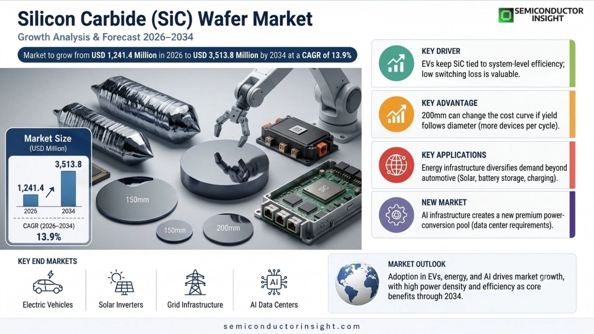
Silicon Carbide (SiC) Wafer Market is estimated at USD 1,241.4 million in 2026, and is projected to reach USD 3,513.8 million by 2034, CAGR of 13.9% during 2026–2034.

PDF Icon Download Sample Report PDF
  • Quick Dispatch

    All Orders

  • Secure Payment

    100% Secure Payment

Price range: $1,500.00 through $4,250.00

Clear

Key Statistics

2025 Market Size
USD 1,090.0 million
2026 Estimated Size
USD 1,241.4 million
2034 Projected Size
USD 3,513.8 million
CAGR (2026–2034)
13.9%
Largest Market in 2025
Asia Pacific

Key Takeaways

  • Asia Pacific is the largest regional market because Japan, China, South Korea and Taiwan combine substrate production, power-semiconductor manufacturing and high-volume electronics supply chains; this creates shorter qualification loops between wafer suppliers, epitaxy providers and device fabs.
  • 6-inch wafers remain the commercial volume anchor in established SiC device manufacturing, while 8-inch/200 mm wafers are the strategic growth platform because a larger usable area per wafer can improve device output per run once crystal quality, epi uniformity and fab yield reach production targets.
  • Power devices are the largest application, led by MOSFETs and diodes used in EV traction inverters, onboard chargers, charging infrastructure, industrial drives, renewable-energy inverters and high-efficiency power supplies where SiC enables higher switching frequency and lower losses.
  • Capacity is constrained upstream by crystal growth rather than ordinary wafer slicing alone. Long boule-growth cycles, defect control, diameter expansion and consistent electrical characteristics determine how quickly nominal wafer capacity becomes qualification-grade supply.
  • The competitive shift is from 150 mm scale to 200 mm industrialization. Wolfspeed, Coherent, ROHM/SiCrystal, SK Siltron and Asian suppliers are using larger-diameter platforms, epitaxy integration and long-term customer qualification to protect strategic positions.
  • Data-center power is broadening the demand mix beyond automotive. 800 VDC architectures, AI power density and high-voltage conversion create a second premium demand pool that can absorb high-quality SiC wafers even when automotive growth is uneven.

Silicon Carbide (SiC) Wafer Market Overview

Silicon Carbide (SiC) Wafer Market was valued at USD 1,090.0 million in 2025, is estimated at USD 1,241.4 million in 2026, and is projected to reach USD 3,513.8 million by 2034, representing an anchor-derived CAGR of 13.9% during 2026–2034. Asia Pacific is the largest regional market in 2025 on the controlling report scope, while the commercial growth mechanism is increasingly shaped by 200 mm capacity qualification, electric-vehicle power electronics, renewable-energy conversion and higher-voltage data-center power architectures.

Base year: 2025 · Estimated year: 2026 · Forecast period: 2026–2034 · Values in USD million unless otherwise stated

Silicon carbide wafers are single-crystal substrates used to fabricate wide-bandgap semiconductor devices. Compared with conventional silicon, SiC supports higher electric fields, higher operating temperatures and faster switching, which allows power-electronic systems to reduce conduction and switching losses and shrink passive components. The wafer therefore sits at the beginning of a performance-critical chain: crystal defects, micropipes, basal-plane dislocations, surface damage and epitaxial uniformity can directly influence downstream device yield and reliability.

The controlling report page defines the market across 4-inch, 6-inch and 8-inch wafer classes and applications spanning power devices, electronics and optoelectronics, wireless infrastructure and other uses. The commercial center of gravity is power electronics, where automotive electrification and energy conversion have created enough device value to justify the more demanding crystal-growth economics of SiC. The transition to 200 mm is now adding a manufacturing-efficiency dimension to the technology case.

Market expansion is not simply a function of more wafer starts. Customers qualify a specific substrate diameter, crystal quality, resistivity profile, orientation, surface finish and epitaxial stack for a defined device flow. Moving from 150 mm to 200 mm therefore requires coordinated changes in boule growth, slicing, polishing, epitaxy, automation, metrology and device-fab process control. Suppliers that can deliver stable lots through those qualification steps gain a stronger position than suppliers offering nominal capacity without repeatable device yield.

Supply economics are also changing as major producers integrate more of the chain. STMicroelectronics has committed to an integrated 200 mm SiC campus in Catania, while Wolfspeed has commercialized a 200 mm materials portfolio and is extending its platform toward 300 mm development. ROHM has emphasized an 8-inch substrate and device transition. These investments make diameter migration a competitive weapon because scale, learning curves and captive demand can reinforce one another.

Segment Analysis: By Type

By wafer size, the source scope covers 4 Inch, 6 Inch and 8 Inch SiC wafers. Six-inch wafers remain the established production workhorse, while 8-inch/200 mm is the fastest-developing strategic format as manufacturers seek more die per wafer and compatibility with automated high-volume power-device fabs.

Type Technical role Market position
4 Inch A mature smaller-diameter format used in legacy, specialty, R&D and lower-volume production. It offers relatively accessible crystal-growth control but yields fewer devices per wafer and is increasingly disadvantaged where customers are standardizing automated production around larger tools. A declining share of new high-volume capacity. Four-inch remains relevant for installed equipment, development work and selected specialty devices, but new strategic investment is directed mainly toward 150 mm and 200 mm platforms.
6 Inch The current high-volume workhorse for SiC MOSFETs, Schottky diodes and other power devices. The format has an established ecosystem across crystal growth, polishing, epitaxy, device processing and metrology, allowing customers to leverage mature recipes and qualification histories. Largest commercial format. Six-inch combines mature yields with broad equipment availability and remains central to automotive and industrial power supply, although its share will be diluted as 200 mm factories ramp.
8 Inch A 200 mm format intended to increase usable die output per wafer and improve compatibility with more automated semiconductor manufacturing. The economic benefit depends on maintaining crystal quality, radial doping control, wafer flatness and epitaxial uniformity across the larger area. Fastest-growing strategic format. Commercial launches, integrated 200 mm campuses and customer qualification programs show that the industry is moving beyond demonstrations toward production, making 8-inch capability a major supplier-selection criterion.

Why is the 200 mm transition commercially important?

A larger wafer can carry materially more die, but the cost advantage appears only if defect density, edge exclusion, bow/warp, polishing quality and epitaxial uniformity remain controlled. This makes the 200 mm transition a manufacturing-learning race rather than a simple geometry change. Suppliers with vertically integrated crystal growth, wafer finishing and epitaxy can use process feedback to improve yields faster, while device makers benefit from greater automation and more output per tool cycle once qualifications stabilize.

Segment Analysis: By Application

By application, the source page segments demand into Power Device, Electronics & Optoelectronics, Wireless Infrastructure and Others. Power devices dominate because SiC’s high-field and high-temperature properties translate directly into system-level efficiency and power-density gains in EVs, industrial conversion, renewable energy and increasingly AI data-center power.

Application Demand characteristics
Power Device Largest application. SiC MOSFETs and diodes are used where switching losses, voltage rating, thermal performance and system size have high economic value. EV traction inverters and onboard chargers remain major demand engines, while solar, storage, industrial drives, charging and data-center power broaden utilization and reduce dependence on one end market.
Electronics & Optoelectronics SiC substrates can support specialized high-temperature electronics, sensing and optoelectronic architectures where thermal conductivity, chemical stability or lattice properties are valuable. Volumes are smaller than mainstream power applications, but qualification requirements can support premium pricing and technically differentiated supply.
Wireless Infrastructure Semi-insulating SiC substrates are relevant to high-frequency RF systems because thermal conductivity helps remove heat from high-power devices. Demand is linked to base-station and communications infrastructure cycles and competes with alternative substrate technologies, making electrical resistivity and defect control particularly important purchasing criteria.
Others Research, aerospace, defense and emerging high-voltage applications create a diversified tail of demand. These programs often value reliability and performance over unit cost, but volumes can be project-based and qualification timelines long, so they support specialized suppliers rather than driving market scale alone.

How is the demand mix broadening beyond electric vehicles?

Automotive electrification created the first large-volume premium case for SiC, but renewable-energy inverters, battery storage, charging infrastructure, industrial power and AI data-center power conversion now provide additional growth vectors. This matters commercially because substrate suppliers can balance automotive cycles with applications that have different investment cadences. High-voltage 800 VDC data-center architectures are especially important because the value of efficiency rises rapidly as rack power density increases.
Silicon Carbide (SiC) Wafer Market Outlook

Regional Analysis

Asia Pacific leads the global SiC wafer market, supported by Japanese materials expertise, Chinese EV and power-device scale, South Korean substrate investment and Taiwan’s broader semiconductor manufacturing ecosystem. North America remains strategically important through Wolfspeed and device innovation, while Europe combines automotive demand with integrated SiC manufacturing investments.

How does SiC wafer demand differ by region?

Regional demand reflects different positions in the value chain. Asia Pacific combines substrate production with the world’s deepest electronics and EV manufacturing ecosystem. North America is technology- and capacity-led, with large materials investments and data-center power demand. Europe is automotive- and industrial-led and is building more vertically integrated SiC capacity. South America and Middle East & Africa are smaller direct wafer markets, with demand primarily transmitted through energy, mobility and industrial equipment supply chains.

Region Position Growth outlook Demand profile What decides supplier selection
Asia Pacific Largest Highest commercial scale Substrate + device + EV ecosystem Quality consistency, price, local qualification, diameter roadmap and supply assurance
North America Strategic technology center High Materials capacity + AI/data-center power 200 mm quality, long-term supply, device yield and domestic capacity
Europe Major integrated market High Automotive + industrial + renewable power Automotive qualification, vertical integration, traceability and 200 mm readiness
South America Emerging downstream demand Moderate from small base Renewable energy + industrial electrification Landed cost, distribution support and application availability
Middle East & Africa Emerging project market Moderate from small base Solar, storage, data centers and infrastructure Project qualification, high-temperature reliability and supply continuity
Asia Pacific LARGEST & FASTEST-GROWING

Why does Asia Pacific lead SiC wafer demand and supply?

Asia Pacific combines major substrate suppliers, power-device manufacturers and the world’s largest EV and electronics production ecosystems. Japan contributes deep crystal and materials expertise; China provides scale in EVs, renewable power and domestic SiC capacity; South Korea has invested in larger-diameter substrates; and Taiwan’s semiconductor infrastructure shortens the path from material qualification to high-volume device manufacturing.

Market positionLargest region
Growth outlookHighest commercial scale
Demand profileEV + power semiconductor manufacturing
Market access gateQualification yield and supply consistency
Country / market Position in region Evidence-led demand logic
China Demand and capacity scale China’s EV, charging, solar and industrial-electronics base creates substantial downstream pull for SiC power devices. Domestic substrate and device makers are also adding capacity, so suppliers compete not only on wafer price but on defect density, 150 mm/200 mm roadmaps and the ability to support rapid customer qualification.
Japan Materials and device expertise Japan hosts established SiC materials and device players including ROHM/SiCrystal and Coherent operations, supported by a broad precision-materials ecosystem. Customers place high value on crystal quality, traceability and long reliability histories because automotive and industrial qualification can lock a wafer platform into production for years.
South Korea & Taiwan Scaling semiconductor ecosystem South Korea has pursued SiC wafer capacity through SK Siltron, while Taiwan contributes foundry, packaging and electronics manufacturing depth. These markets are important for translating wafer technology into repeatable device output, particularly as 200 mm automation and equipment compatibility become more commercially significant.
2026 – ROHM emphasizes 8-inch transition

ROHM’s FY2025 materials identify a strategy of focusing the substrate business on 8-inch SiC while reducing in-house 6-inch exposure and aligning device production with newer technology generations. The move illustrates how Japanese suppliers are reallocating capital toward diameter scale rather than simply expanding legacy formats.

Market relevance: The shift raises competitive pressure on all regional suppliers to prove 200 mm crystal quality and cost performance, and it increases the value of customers that can qualify new wafer diameters early.

2026 – China EV and renewable power sustain pull

Asia’s high-volume EV, charging and solar supply chains continue to create multiple outlets for SiC power devices rather than relying on a single appliance or industrial cycle. The breadth of downstream applications helps absorb wafer capacity and supports local qualification ecosystems.

Market relevance: A diversified end-use base improves utilization prospects for substrate makers and encourages device manufacturers to secure multi-year access to high-quality wafers.

2025–2026 – 200 mm becomes an industry benchmark

Commercial 200 mm materials launches and integrated factory investments globally establish a new benchmark that Asian suppliers must match. Even where 150 mm remains profitable, customers increasingly evaluate vendors on their 200 mm roadmap because future device cost and fab automation depend on the transition.

Market relevance: Qualification readiness is becoming a market-access requirement, accelerating equipment, metrology and epitaxy investment across the region.

Full-report coverage: Country-level revenue, sales, supplier positioning and forecast detail are retained in the full study; this overview highlights the countries with the clearest, independently supportable demand mechanisms.
North America TECHNOLOGY & CAPACITY HUB

What makes North America strategically important in SiC wafers?

North America is strategically important because Wolfspeed combines large-scale SiC crystal expertise with a commercial 200 mm materials roadmap, while U.S. demand is expanding from automotive power into AI data-center power conversion. The region’s value lies less in broad electronics assembly volume than in materials IP, advanced power-device architectures and customers willing to pay for efficiency at high system power.

Market positionStrategic technology center
Growth outlookHigh
Demand profileMaterials + AI power + EV
Market access gate200 mm quality and long-term qualification
Country / market Position in region Evidence-led demand logic
United States Materials and high-power demand hub The U.S. hosts Wolfspeed’s SiC materials and device programs and a rapidly growing AI data-center market that values efficient high-voltage conversion. Customer selection therefore centers on stable 200 mm supply, device-grade epitaxy, qualification data and the ability to support long platform lifecycles rather than on commodity wafer pricing alone.
Canada Smaller specialized demand Canada’s direct SiC wafer consumption is smaller, but power electronics research, clean-energy systems and industrial applications create specialized demand. Supply typically depends on North American distribution and cross-border semiconductor ecosystems, so access to qualified wafers matters more than domestic crystal capacity.
Mexico Automotive electronics linkage Mexico’s automotive manufacturing base creates indirect demand through traction, charging and power-electronics supply chains. Most wafer processing occurs elsewhere, but vehicle-platform localization can influence device sourcing and encourages suppliers to maintain reliable North American logistics.
13 January 2026 – Wolfspeed demonstrates 300 mm SiC

Wolfspeed announced a 300 mm single-crystal SiC technology breakthrough, extending the diameter roadmap beyond current 200 mm commercialization. The achievement does not mean immediate mass production, but it demonstrates that crystal-growth and wafer-processing learning is continuing beyond the current transition.

Market relevance: The announcement strengthens North America’s technology position and signals that diameter scale will remain a long-term competitive axis for wafer suppliers.

10 March 2026 – 300 mm SiC linked to AI packaging

Wolfspeed connected its 300 mm SiC technology platform with next-generation AI data-center advanced packaging, highlighting potential use of SiC’s thermal and electrical properties in high-density computing environments.

Market relevance: The development broadens the strategic relevance of SiC materials beyond classical discrete power devices and gives suppliers another premium application path tied to AI infrastructure.

10 September 2025 – commercial 200 mm materials launch

Wolfspeed commercially launched a 200 mm SiC materials portfolio and made 200 mm epitaxial wafers available for customer qualification. The transition moved larger-diameter material from development status toward a purchasable production platform.

Market relevance: Commercial availability increases customer options for 200 mm device programs and turns wafer uniformity, defect performance and delivery scale into measurable procurement criteria.

Full-report coverage: Country-level revenue, sales, supplier positioning and forecast detail are retained in the full study; this overview highlights the countries with the clearest, independently supportable demand mechanisms.
Europe AUTOMOTIVE & INTEGRATED MANUFACTURING

Why is Europe important to the SiC wafer market?

Europe combines premium automotive electrification, industrial power systems and renewable-energy conversion with a policy-backed effort to localize semiconductor manufacturing. The most important structural change is vertical integration: device makers are investing in substrate, device, testing and packaging capability so they can control both supply risk and process learning as the industry moves to 200 mm.

Market positionMajor integrated market
Growth outlookHigh
Demand profileAutomotive + industrial
Market access gateQualification, traceability and 200 mm readiness
Country / market Position in region Evidence-led demand logic
Italy Integrated SiC manufacturing center STMicroelectronics is building an integrated 200 mm SiC campus in Catania covering substrate development, device fabrication and downstream process steps. This creates a local feedback loop between wafer characteristics and device yield and reduces dependence on externally coordinated supply chains.
Germany Automotive and industrial demand Germany’s automotive OEMs, Tier-1 suppliers and industrial automation base create strong demand for SiC devices used in traction, charging, motor drives and energy conversion. Suppliers must meet long automotive qualification cycles and demonstrate repeatable quality rather than compete solely on wafer cost.
France & broader EU Power electronics and policy support European semiconductor policy and electrification targets support investment in power electronics, while aerospace, rail, industrial and renewable applications diversify demand. EU customers place additional weight on supply-chain resilience and traceability, which can favor qualified regional capacity.
31 May 2024 – ST announces Catania 200 mm SiC campus

STMicroelectronics announced a new integrated 200 mm silicon-carbide manufacturing facility in Catania, with approximately €5 billion of multi-year investment and Italian state support under the EU Chips Act framework. The campus is designed to cover substrate, device, test and packaging activities.

Market relevance: Integration can shorten learning cycles between wafer quality and finished-device yield while improving European supply resilience for automotive and industrial customers.

2025–2026 – automotive platforms continue SiC qualification

European vehicle electrification keeps SiC qualification tied to multi-year automotive programs where reliability, efficiency and supply continuity are tightly specified. Once a wafer platform is qualified into a power module, switching suppliers carries substantial revalidation cost.

Market relevance: This favors vendors with stable crystal quality, long-term capacity commitments and local technical support, raising barriers to opportunistic wafer entrants.

2026 – 200 mm readiness becomes procurement criteria

As global suppliers commercialize 200 mm wafers, European device makers increasingly evaluate future substrate sources on diameter roadmap and automation compatibility even when current products still use 150 mm material.

Market relevance: The shift encourages capital spending before 200 mm becomes the majority format because customers want qualified alternatives available ahead of production transfers.

Full-report coverage: Country-level revenue, sales, supplier positioning and forecast detail are retained in the full study; this overview highlights the countries with the clearest, independently supportable demand mechanisms.
South America RENEWABLE-ENERGY LED

What drives South American SiC wafer-linked demand?

South America is a small direct wafer-processing market, but renewable-energy projects, electric mobility and industrial modernization create downstream demand for SiC-containing inverters, chargers and power modules. The region therefore participates mainly through imported semiconductor devices and systems, with wafer demand captured upstream in the manufacturing regions that supply those products.

Market positionSmaller direct market
Growth outlookModerate from small base
Demand profileSolar + industry + mobility
Market access gateLanded system cost and distributor support
Country / market Position in region Evidence-led demand logic
Brazil Largest downstream opportunity Brazil’s large industrial base, solar additions and emerging vehicle electrification create demand for efficient power conversion. Direct wafer consumption is limited, so commercial impact is transmitted through imported inverters, power modules and charging systems rather than domestic SiC crystal growth.
Chile Renewable-power use case Chile’s solar and mining sectors create high-value power-conversion requirements where efficiency, temperature performance and reliability matter. Suppliers benefit when SiC devices reduce cooling or conversion losses in remote or high-utilization infrastructure.
Argentina Selective industrial demand Argentina provides smaller project-based opportunities in industrial drives, energy and transport. Currency and investment cycles can make demand uneven, so supplier success depends on channel availability and project economics more than local semiconductor manufacturing capacity.
2026 – utility-scale renewable projects expand conversion needs

Continued solar, storage and grid investment increases the number of high-power conversion stages deployed across the region. SiC content is determined by inverter and power-module design choices made by global equipment suppliers rather than by local wafer buyers.

Market relevance: Regional energy investment adds incremental wafer demand upstream while keeping procurement concentrated in established semiconductor manufacturing hubs.

2026 – EV and charging ecosystems develop selectively

Brazil and other markets are adding electric vehicles and charging infrastructure, creating a growing installed base of SiC-relevant power electronics even though adoption rates differ by country.

Market relevance: The opportunity favors global device vendors and their qualified wafer suppliers because automotive platforms are usually sourced internationally.

2025–2026 – mining and industrial efficiency remain premium niches

Mining, motor drives and remote-energy systems can justify higher-efficiency power electronics where downtime, heat and energy losses are costly.

Market relevance: These use cases support premium SiC devices and create less price-sensitive demand than mass consumer electronics, although total wafer-equivalent volume remains modest.

Full-report coverage: Country-level revenue, sales, supplier positioning and forecast detail are retained in the full study; this overview highlights the countries with the clearest, independently supportable demand mechanisms.
Middle East & Africa INFRASTRUCTURE & HIGH-TEMPERATURE OPPORTUNITY

Where does SiC fit in Middle East and African markets?

Direct SiC wafer manufacturing is limited, but the region has compelling downstream conditions: utility solar, battery storage, EV charging, industrial infrastructure and rapidly expanding data centers. High ambient temperatures and large power flows increase the economic value of efficient conversion, so SiC can gain content in imported inverters and power systems even without a local substrate ecosystem.

Market positionSmall direct wafer base
Growth outlookModerate from small base
Demand profileSolar + data centers + infrastructure
Market access gateSystem qualification and harsh-environment reliability
Country / market Position in region Evidence-led demand logic
United Arab Emirates Data center and infrastructure growth The UAE’s data-center, transport and clean-energy investments create demand for efficient high-voltage conversion. The commercial opportunity reaches wafer suppliers indirectly through global power-semiconductor and equipment vendors chosen for large infrastructure projects.
Saudi Arabia Large power and industrial projects Saudi industrial diversification, renewable-energy investment and data-center development increase the number of high-power conversion applications. Heat tolerance and efficiency can strengthen the system case for SiC, while procurement remains project-led and specification-driven.
South Africa Renewable and grid-resilience demand Solar, storage and industrial power systems create opportunities for SiC-enabled inverters and converters. Local wafer production is not the driver; the market effect comes from imported equipment and semiconductor modules selected for efficiency and reliability.
2026 – AI and data-center buildout raises power-conversion intensity

Large planned computing campuses increase the value of high-voltage, high-efficiency power distribution because energy lost in conversion adds directly to operating cost and thermal load.

Market relevance: SiC adoption in 800 VDC and other high-voltage architectures can create premium wafer demand upstream even when the final data-center project is located far from substrate production.

2025–2026 – solar and storage remain core conversion markets

Utility renewable projects require repeated DC/DC and DC/AC conversion stages where higher switching frequency and lower losses can reduce system size and improve efficiency.

Market relevance: Project specifications can increase SiC device content, benefiting qualified wafer suppliers through global inverter makers.

2026 – harsh ambient conditions reward thermal performance

High-temperature industrial and infrastructure environments raise the value of wide-bandgap devices that can operate efficiently with lower cooling burden.

Market relevance: The commercial effect is strongest in high-utilization equipment where lifecycle energy and reliability outweigh the premium semiconductor cost.

Full-report coverage: Country-level revenue, sales, supplier positioning and forecast detail are retained in the full study; this overview highlights the countries with the clearest, independently supportable demand mechanisms.

Competitive Landscape

Competition is defined by crystal-growth know-how, defect density, diameter transition, epitaxy integration and customer qualification. The source scope includes established global materials groups, vertically integrated device makers and fast-scaling Asian substrate suppliers; commercial leadership depends on converting boule capacity into repeatable device-grade wafers rather than on nominal furnace count alone.

The hardest capability to replicate is stable single-crystal growth at larger diameters. Increasing boule diameter can amplify thermal-stress and defect-control challenges, so experience accumulated over many growth cycles matters. Suppliers with strong feedback between crystal growth, slicing, polishing, characterization and epitaxy can identify yield loss earlier and improve lot consistency faster.

Vertical integration is increasingly important. Wolfspeed and ST link material development to downstream device manufacturing, while ROHM combines SiCrystal substrate capability with power-device demand. This can secure captive utilization and accelerate learning, but independent suppliers remain important because device makers want second sources and flexible procurement rather than dependence on one vertically integrated competitor.

Asian suppliers are increasing competitive intensity by localizing substrate capacity closer to the largest EV and power-electronics manufacturing bases. Their opportunity is strongest where customers prioritize rapid engineering support and cost reduction, but qualification barriers remain high: low headline wafer price has limited value if defects reduce expensive device yield.

The 200 mm transition creates a temporary window for share shifts. A supplier that qualifies reliable 200 mm material early can enter new fabs and production lines before recipes become locked, while a supplier late to the transition risks being confined to replacement demand on 150 mm platforms. Commercial 200 mm launches therefore carry strategic importance beyond their initial shipment volume.

Competitive tier Representative companies Commercial basis
Integrated technology leaders Wolfspeed; STMicroelectronics; ROHM Group (SiCrystal) Combine substrate know-how with device manufacturing or deep power-semiconductor integration, enabling rapid feedback between wafer characteristics and device yield.
Global materials specialists Coherent Corp.; SK Siltron; GlobalWafers Co. Ltd.; Showa Denko Materials Compete through crystal-growth scale, materials science, diameter roadmaps, epitaxial capability and ability to support multiple device customers.
Scaling Asian specialists TankeBlue Semiconductor; SICC; Sanan Semiconductor; Hangzhou Lijing Microelectronics; Hebei Synlight Crystal; PAM-XIAMEN Target localization, cost competitiveness and rapid capacity growth while building the defect-control and qualification track record required by automotive and industrial customers.

Companies profiled in the source scope

Wolfspeed, Coherent Corp., ROHM Group (SiCrystal), SK Siltron, TankeBlue Semiconductor, SICC (Beijing Superconductor Technology), Sanan Semiconductor, Showa Denko Materials, Fuji Electric, II-VI Incorporated (now part of Coherent), GlobalWafers Co. Ltd., STMicroelectronics, Hangzhou Lijing Microelectronics, Hebei Synlight Crystal, Xiamen Powerway Advanced Material (PAM-XIAMEN).

Production Capacity Analysis

SiC wafer capacity is concentrated around high-temperature crystal growth, wafer finishing and epitaxy. The real bottleneck is not simply adding tools: suppliers must grow larger low-defect boules repeatedly, recover usable wafers efficiently and deliver surface and epi characteristics that support high-value power-device yield.

Crystal growth is capital- and learning-intensive because SiC is produced at very high temperatures and defects formed during boule growth cannot be repaired later by polishing. Larger diameters increase the economic prize but also increase the area over which stress, doping and crystallographic quality must remain controlled. This makes qualified output a more meaningful capacity measure than installed furnace count.

After growth, boules are sliced, ground and polished to semiconductor tolerances. Kerf loss and wafer breakage directly affect material economics because the upstream crystal is expensive. Surface damage also matters because the wafer often receives epitaxy before device processing; subsurface defects or nonuniform polishing can propagate into yield loss at a much more valuable downstream step.

Epitaxy is strategically important because many device customers prefer a qualified epi-ready or epitaxial wafer rather than a bare substrate. Uniform thickness, doping and defect conversion across 200 mm become increasingly demanding. Suppliers able to integrate substrate and epitaxy can capture more value and provide device fabs with fewer interfaces to manage.

Capacity layer Where it concentrates Commercial constraint
Single-crystal boule growth United States, Japan, China, South Korea and selected European capacity Diameter scale, defect density, thermal control and long growth cycles limit how quickly qualified output can expand.
Slicing and polishing Co-located with substrate producers or specialty wafer processors Kerf loss, wafer bow/warp, surface damage and breakage determine how much expensive crystal becomes saleable wafer area.
Epitaxy Integrated material suppliers and specialist epi houses near device fabs Radial thickness and doping uniformity, defect conversion and customer-specific epi stacks are critical for device yield.
200 mm qualification New and upgraded high-volume SiC lines Tool compatibility, automated handling, metrology and repeatable multi-lot device results gate conversion from engineering samples to production.

Market Dynamics

Market growth is driven by the system value of lower-loss high-voltage power conversion, but restrained by the physics and economics of producing low-defect SiC at scale. The strongest commercial winners will be suppliers that translate 200 mm technology into stable qualified output while diversifying demand across automotive, energy, industrial and data-center customers.

Market Drivers

Factor Directional impact Why it matters
EV power-electronics penetration High Traction inverters, onboard chargers and fast-charging systems create high-value demand for SiC MOSFETs and diodes, directly pulling substrate and epitaxial wafer volumes.
200 mm manufacturing transition High Larger wafers can increase die output per process cycle and improve automation economics once material quality and device yield are stable.
Renewable energy and storage Medium-High Solar, battery storage and grid conversion reward lower switching losses and higher power density across high-utilization inverter systems.
AI data-center power density Medium-High 800 VDC and high-voltage power architectures increase the value of efficient switching as rack and campus power requirements rise.

Electric vehicles keep SiC tied to system-level efficiency

SiC’s value in EVs is measured through range, inverter size, cooling burden and charging performance rather than through semiconductor cost alone. When vehicle platforms move to higher battery voltage, lower switching loss and high-temperature capability become more valuable. This supports premium wafer demand because device makers can justify higher substrate cost when it contributes to a measurable vehicle-level efficiency or packaging advantage.

200 mm can change the cost curve if yield follows diameter

Moving from 150 mm to 200 mm increases wafer area substantially, creating the possibility of more devices per processing cycle and better use of automated fabs. The qualification hurdle is equally larger: defect density, flatness and epi uniformity must remain controlled over more area. Successful 200 mm suppliers can therefore gain both technology credibility and a structural cost advantage.

Energy infrastructure diversifies demand beyond automotive cycles

Solar, battery storage, charging, industrial motor drives and grid equipment operate for long hours and process significant power, making efficiency losses economically visible. These applications create a steadier demand layer than consumer electronics and broaden the customer base for SiC wafers, reducing dependence on the timing of individual vehicle-platform ramps.

AI infrastructure creates a new premium power-conversion pool

AI data centers are pushing rack and campus power requirements sharply upward. As distribution architectures move toward higher DC voltages, conversion efficiency and thermal management become core design constraints. SiC devices can address those constraints, creating incremental demand for high-quality wafers and giving materials suppliers another growth market with high willingness to pay for performance.

Market Restraints

Factor Directional impact Why it matters
Crystal defects and yield variability High Substrate defects can reduce expensive device yield, so customers qualify material slowly and penalize inconsistency more heavily than nominal wafer price.
200 mm capital and process transition High New crystal, polishing, epi, metrology and device-fab processes require investment before larger-diameter economics are fully proven.
Automotive demand cyclicality and inventory corrections Medium A large automotive exposure can produce utilization swings when EV platform schedules, inventories or end-demand expectations change.
Competing wide-bandgap technologies Medium GaN and improved silicon devices can serve portions of the power market, limiting SiC penetration where voltage, thermal or efficiency advantages do not justify cost.

Crystal quality remains the fundamental supply constraint

SiC wafers cannot be treated as commodity silicon. Dislocations, micropipes and other defects formed in the crystal can affect downstream device performance and reliability, and the cost of discovering a poor wafer after epitaxy and device processing is high. Customers therefore demand lot consistency and detailed characterization, which slows qualification and makes rapid capacity expansion difficult.

The 200 mm transition requires synchronized investment

A larger substrate is useful only when crystal growth, slicing, polishing, epitaxy, metrology and device-fab equipment are all ready. Mismatched readiness can leave nominal material capacity underutilized or force customers to run lengthy engineering programs. Suppliers must finance this transition before mature 200 mm economics are guaranteed, increasing capital intensity.

Automotive concentration can create utilization volatility

Automotive electrification is a powerful structural driver, but vehicle programs are exposed to model launches, inventory corrections, subsidy changes and regional demand shifts. A substrate supplier built around one or two major automotive ramps can face abrupt utilization changes, making application diversification into energy and data centers strategically valuable.

Alternative devices constrain the addressable voltage-performance envelope

SiC is not the lowest-cost answer for every converter. Silicon remains economical in many mature power ranges, while GaN can be attractive in high-frequency lower-voltage applications. SiC wafer demand therefore depends on device architectures where its voltage, temperature and efficiency advantages are large enough to offset higher material and processing cost.

Market Opportunities

200 mm production qualification

The highest-value near-term opportunity is to qualify repeatable 200 mm substrate and epitaxial wafer supply with multiple power-device customers. A successful qualification can lock a supplier into an entire device-family lifecycle and give it reference data for additional fabs. The commercial prize is not just larger wafers; it is participation in new production lines before the approved vendor set becomes fixed.

AI data-center 800 VDC power

Rapidly rising data-center power density creates an application where small efficiency gains translate into large energy and cooling savings. Suppliers that can connect SiC material quality to reliable high-voltage devices for 800 VDC distribution and conversion can access a premium customer base less tied to automotive cycles.

Regional supply resilience

Device manufacturers in Europe, North America and Asia increasingly value secure, geographically diversified semiconductor supply. Qualified second-source wafer capacity can command strategic importance even when it is not the absolute lowest-cost option, creating opportunities for suppliers that combine local technical support with credible long-term capacity.

Semi-insulating and specialty substrates

Beyond mainstream conductive power-device wafers, semi-insulating SiC supports high-frequency and specialized electronic applications. These niches are smaller but can reward tight resistivity control, thermal performance and low defect density, allowing technically strong suppliers to capture margin without competing purely on automotive-scale volume.

Supply Chain Analysis

1. Raw SiC & crystal growthHigh-purity source material is converted into single-crystal boules under tightly controlled high-temperature conditions.
2. Wafer fabricationBoules are sliced, ground, polished and characterized into 100 mm, 150 mm and increasingly 200 mm device-grade substrates.
3. Epitaxy & device fabricationCustomers add controlled epitaxial layers and fabricate MOSFETs, diodes, RF devices and other wide-bandgap semiconductors.
4. Modules & power systemsDevices are packaged into traction, charging, renewable-energy, industrial and data-center power systems where efficiency creates end-user value.

Crystal growth. Value capture begins with proprietary furnace conditions, seed control and defect-reduction know-how. Growth cycles are long and the crystal is expensive, so yield at this stage determines the economics of every downstream wafer. Larger diameters magnify both the opportunity and the cost of poor process control.

Wafer fabrication. Slicing and polishing convert each boule into saleable area. Suppliers seek to reduce kerf loss, breakage and subsurface damage while meeting tight bow, warp and surface specifications. Because a polished wafer carries significant embedded crystal cost, modest yield improvements can materially affect gross margin.

Epitaxy and device manufacturing. Epitaxial growth adds application-specific doping and thickness profiles and is a major quality gate before device fabrication. Device fabs then impose their own qualification standards, so substrate suppliers that understand downstream yield can optimize specifications around actual commercial value rather than laboratory metrics alone.

Modules and systems. The final economic case is created at system level. Automotive inverters, solar systems, chargers and data centers pay for lower losses, smaller cooling systems and higher power density. That system value supports premium semiconductor pricing, which in turn sustains the more expensive SiC wafer supply chain.

Recent Developments in the Silicon Carbide (SiC) Wafer Market

Developments tracked to September 2026. Entries are dated to the official publication date where available.

  • 6 August 2026 Data-center expansion
    Wolfspeed and LITEON announced collaboration around next-generation 800 VDC AI data-center power architectures, extending the commercial demand case for SiC beyond automotive traction. Higher DC distribution voltage increases the importance of efficient, high-voltage switching and can create a premium growth outlet for qualified SiC substrate and device capacity. Source
  • 9 June 2026 Technology generation
    Wolfspeed introduced a new generation of SiC MOSFET technology alongside its 200 mm manufacturing platform. The product move matters to wafers because device performance, cost and substrate utilization increasingly develop together; customers evaluating larger diameters need evidence that material scale translates into competitive finished devices. Source
  • 10 March 2026 AI packaging
    Wolfspeed outlined a foundation for next-generation AI data-center advanced packaging using 300 mm SiC technology. Although 300 mm remains ahead of mainstream wafer production, the announcement demonstrates a longer diameter roadmap and broadens SiC’s role from discrete power conversion toward thermal and packaging challenges in AI systems. Source
  • 13 January 2026 Diameter breakthrough
    Wolfspeed announced a 300 mm single-crystal SiC technology breakthrough, showing that crystal-growth learning is extending beyond the industry’s current 200 mm transition. The milestone reinforces diameter capability as a long-term competitive differentiator and raises expectations for suppliers still working to industrialize 200 mm output. Source
  • 10 September 2025 Commercial launch
    Wolfspeed commercially launched its 200 mm SiC materials portfolio and made 200 mm epitaxial wafers available for qualification. The move is important because it converts larger-diameter SiC from a development milestone into a commercial sourcing option, forcing competing suppliers to prove uniformity, defect performance and customer-ready scale. Source

Report Scope & Segmentation

Attribute Coverage
Report title Silicon Carbide (SiC) Wafer Market, Global Business Strategies 2025-2032
Base / estimate / forecast 2025 base year; 2026 estimated year; 2034 forecast end year; CAGR measured for 2026–2034.
By Type 4 Inch; 6 Inch; 8 Inch.
By Application Power Device; Electronics & Optoelectronics; Wireless Infrastructure; Others.
By Technology Conductive SiC; Semi-insulating SiC; epitaxy-ready polished wafer configurations, as applicable to the source discussion.
By End User Automotive; Energy & utilities; Industrial and other power-electronics customers, aligned with the source-page demand discussion.
Regions North America, Europe, Asia-Pacific, South America, and Middle East & Africa, with country-level analysis where relevant to the source scope.
Companies Wolfspeed, Coherent Corp., ROHM Group (SiCrystal), SK Siltron, TankeBlue Semiconductor, SICC (Beijing Superconductor Technology), Sanan Semiconductor, Showa Denko Materials, Fuji Electric, II-VI Incorporated (now part of Coherent), GlobalWafers Co. Ltd., STMicroelectronics, Hangzhou Lijing Microelectronics, Hebei Synlight Crystal, Xiamen Powerway Advanced Material (PAM-XIAMEN)
Customization Scope Free report customization (equivalent to up to 4 analyst working days) with purchase. Addition or alteration to country, regional and segment scope.

Frequently Asked Questions

What is the size of the silicon carbide wafer market?

Using the source page’s published USD 1,090 million value for 2025 and USD 2,709 million endpoint for 2032, the internally consistent series gives an estimated USD 1,241.4 million in 2026 and approximately USD 3,513.8 million by 2034. The anchor-derived CAGR is 13.9% during 2026–2034. The body-published 2025 value is preserved because it already matches the target base year.

Which wafer size leads the SiC market?

6-inch wafers remain the established commercial workhorse because device fabs have mature equipment, epitaxy and qualification histories around the format. However, 8-inch or 200 mm wafers are the industry’s strategic growth platform because they can increase die output per process cycle once defect density, flatness and epitaxial uniformity are controlled at production scale.

Why are 200 mm SiC wafers important?

Two hundred millimeter wafers offer more usable area and can improve compatibility with highly automated semiconductor manufacturing, creating a path to lower device cost. The benefit is conditional: larger crystals must maintain low defect density, controlled bow and warp, consistent electrical properties and uniform epitaxy. As a result, 200 mm qualification is a test of manufacturing maturity rather than wafer diameter alone.

What is the largest application for SiC wafers?

Power devices are the largest application in the source scope. SiC substrates are used for MOSFETs, Schottky diodes and related devices in EV traction, onboard charging, renewable-energy inverters, industrial drives and high-voltage power supplies. The substrate premium is justified where lower switching loss, higher voltage capability and reduced cooling burden create system-level economic value.

Which region leads the SiC wafer market?

Asia Pacific is the largest regional market because it combines major substrate suppliers with high-volume EV, power-semiconductor and electronics manufacturing. Japan contributes materials expertise, China provides very large downstream power-electronics demand and local capacity, and South Korea and Taiwan add semiconductor process scale that shortens customer qualification and supply-chain response times.

Who are the key companies in the SiC wafer market?

The source page profiles Wolfspeed, Coherent, ROHM Group through SiCrystal, SK Siltron, TankeBlue Semiconductor, SICC, Sanan Semiconductor, Showa Denko Materials, Fuji Electric, GlobalWafers, STMicroelectronics and several Chinese specialty suppliers. Competitive position depends on crystal quality, diameter roadmap, epitaxy capability, customer qualification and the ability to convert installed furnaces into repeatable device-grade output.

What constrains SiC wafer supply?

The main constraint is qualified low-defect crystal growth. SiC boules require demanding high-temperature processes, and defects created during growth can reduce downstream device yield. Slicing, polishing and epitaxy add further yield gates. This means announced furnace capacity can materially exceed the amount of wafer area that customers are willing to qualify for automotive or industrial production.

How does AI data-center growth affect SiC wafers?

AI data centers are increasing rack and campus power density, encouraging higher-voltage distribution and more efficient conversion. SiC devices can reduce switching losses and thermal burden in those architectures, giving wafer suppliers a premium growth outlet beyond automotive. The opportunity is especially relevant to 800 VDC and other high-voltage designs where efficiency gains accumulate across very large continuous power loads.

What is the main competitive trend in SiC wafers?

The central competitive trend is the shift from mature 150 mm production toward 200 mm industrialization. Suppliers are trying to qualify larger-diameter bare and epitaxial wafers while improving defect density and uniformity. Companies that win early 200 mm qualifications can enter new fab platforms before approved-vendor lists become fixed, creating a durable share advantage.

What is the forecast CAGR for the SiC wafer market?

The internally consistent growth rate derived from the controlling USD 1,090 million 2025 and USD 2,709 million 2032 anchors is approximately 13.9% CAGR. Applying that same compound growth factor to the target period produces the 2026 estimate and 2034 forecast used throughout this overview rather than relying on the conflicting printed CAGR label.

Research Sources & Evidence Base

View research sources used for this overview
  1. Wolfspeed. Commercial launch of 200mm silicon carbide materials portfolio, 200 mm commercial availability and qualification context.
  2. Wolfspeed. 300mm silicon carbide technology breakthrough, Long-term diameter roadmap and crystal-growth technology.
  3. Wolfspeed. 300mm SiC technology for AI data-center advanced packaging, AI infrastructure and advanced-packaging opportunity.
  4. STMicroelectronics. New integrated 200mm SiC manufacturing facility in Catania, European integrated capacity, investment and 200 mm manufacturing.
  5. ROHM. FY2025 Financial Results Presentation, 8-inch substrate and device transition strategy.
  6. Coherent. Investor presentation – silicon carbide business overview, 200 mm manufacturing capability and supplier positioning.
  7. Wolfspeed. Artificial Intelligence News, 800 VDC AI data-center power collaboration and demand diversification.
Silicon Carbide (SiC) Wafer Market, Trends, Business Strategies 2026-2034

Get Sample Report PDF for Exclusive Insights

Report Sample Includes

  • Table of Contents
  • List of Tables & Figures
  • Charts, Research Methodology, and more...

PDF Icon Download Sample Report PDF
SKU: f1b9303ca204
Category:

Download Sample Report

Table of Content

1 Introduction to Research & Analysis Reports
1.1 Silicon Carbide (SiC) Wafer Market Definition
1.2 Market Segments
1.2.1 Segment by Type
1.2.2 Segment by Application
1.3 Global Silicon Carbide (SiC) Wafer Market Overview
1.4 Features & Benefits of This Report
1.5 Methodology & Sources of Information
1.5.1 Research Methodology
1.5.2 Research Process
1.5.3 Base Year
1.5.4 Report Assumptions & Caveats
2 Global Silicon Carbide (SiC) Wafer Overall Market Size
2.1 Global Silicon Carbide (SiC) Wafer Market Size: 2024 VS 2032
2.2 Global Silicon Carbide (SiC) Wafer Market Size, Prospects & Forecasts: 2020-2032
2.3 Global Silicon Carbide (SiC) Wafer Sales: 2020-2032
3 Company Landscape
3.1 Top Silicon Carbide (SiC) Wafer Players in Global Market
3.2 Top Global Silicon Carbide (SiC) Wafer Companies Ranked by Revenue
3.3 Global Silicon Carbide (SiC) Wafer Revenue by Companies
3.4 Global Silicon Carbide (SiC) Wafer Sales by Companies
3.5 Global Silicon Carbide (SiC) Wafer Price by Manufacturer (2020-2025)
3.6 Top 3 and Top 5 Silicon Carbide (SiC) Wafer Companies in Global Market, by Revenue in 2024
3.7 Global Manufacturers Silicon Carbide (SiC) Wafer Product Type
3.8 Tier 1, Tier 2, and Tier 3 Silicon Carbide (SiC) Wafer Players in Global Market
3.8.1 List of Global Tier 1 Silicon Carbide (SiC) Wafer Companies
3.8.2 List of Global Tier 2 and Tier 3 Silicon Carbide (SiC) Wafer Companies
4 Sights by Product
4.1 Overview
4.1.1 Segment by Type – Global Silicon Carbide (SiC) Wafer Market Size Markets, 2024 & 2032
4.1.2 4 Inch
4.1.3 6 Inch
4.1.4 8 Inch
4.2 Segment by Type – Global Silicon Carbide (SiC) Wafer Revenue & Forecasts
4.2.1 Segment by Type – Global Silicon Carbide (SiC) Wafer Revenue, 2020-2025
4.2.2 Segment by Type – Global Silicon Carbide (SiC) Wafer Revenue, 2026-2032
4.2.3 Segment by Type – Global Silicon Carbide (SiC) Wafer Revenue Market Share, 2020-2032
4.3 Segment by Type – Global Silicon Carbide (SiC) Wafer Sales & Forecasts
4.3.1 Segment by Type – Global Silicon Carbide (SiC) Wafer Sales, 2020-2025
4.3.2 Segment by Type – Global Silicon Carbide (SiC) Wafer Sales, 2026-2032
4.3.3 Segment by Type – Global Silicon Carbide (SiC) Wafer Sales Market Share, 2020-2032
4.4 Segment by Type – Global Silicon Carbide (SiC) Wafer Price (Manufacturers Selling Prices), 2020-2032
5 Sights by Application
5.1 Overview
5.1.1 Segment by Application – Global Silicon Carbide (SiC) Wafer Market Size, 2024 & 2032
5.1.2 Power Device
5.1.3 Electronics & Optoelectronics
5.1.4 Wireless Infrastructure
5.1.5 Others
5.2 Segment by Application – Global Silicon Carbide (SiC) Wafer Revenue & Forecasts
5.2.1 Segment by Application – Global Silicon Carbide (SiC) Wafer Revenue, 2020-2025
5.2.2 Segment by Application – Global Silicon Carbide (SiC) Wafer Revenue, 2026-2032
5.2.3 Segment by Application – Global Silicon Carbide (SiC) Wafer Revenue Market Share, 2020-2032
5.3 Segment by Application – Global Silicon Carbide (SiC) Wafer Sales & Forecasts
5.3.1 Segment by Application – Global Silicon Carbide (SiC) Wafer Sales, 2020-2025
5.3.2 Segment by Application – Global Silicon Carbide (SiC) Wafer Sales, 2026-2032
5.3.3 Segment by Application – Global Silicon Carbide (SiC) Wafer Sales Market Share, 2020-2032
5.4 Segment by Application – Global Silicon Carbide (SiC) Wafer Price (Manufacturers Selling Prices), 2020-2032
6 Sights by Region
6.1 By Region – Global Silicon Carbide (SiC) Wafer Market Size, 2024 & 2032
6.2 By Region – Global Silicon Carbide (SiC) Wafer Revenue & Forecasts
6.2.1 By Region – Global Silicon Carbide (SiC) Wafer Revenue, 2020-2025
6.2.2 By Region – Global Silicon Carbide (SiC) Wafer Revenue, 2026-2032
6.2.3 By Region – Global Silicon Carbide (SiC) Wafer Revenue Market Share, 2020-2032
6.3 By Region – Global Silicon Carbide (SiC) Wafer Sales & Forecasts
6.3.1 By Region – Global Silicon Carbide (SiC) Wafer Sales, 2020-2025
6.3.2 By Region – Global Silicon Carbide (SiC) Wafer Sales, 2026-2032
6.3.3 By Region – Global Silicon Carbide (SiC) Wafer Sales Market Share, 2020-2032
6.4 North America
6.4.1 By Country – North America Silicon Carbide (SiC) Wafer Revenue, 2020-2032
6.4.2 By Country – North America Silicon Carbide (SiC) Wafer Sales, 2020-2032
6.4.3 United States Silicon Carbide (SiC) Wafer Market Size, 2020-2032
6.4.4 Canada Silicon Carbide (SiC) Wafer Market Size, 2020-2032
6.4.5 Mexico Silicon Carbide (SiC) Wafer Market Size, 2020-2032
6.5 Europe
6.5.1 By Country – Europe Silicon Carbide (SiC) Wafer Revenue, 2020-2032
6.5.2 By Country – Europe Silicon Carbide (SiC) Wafer Sales, 2020-2032
6.5.3 Germany Silicon Carbide (SiC) Wafer Market Size, 2020-2032
6.5.4 France Silicon Carbide (SiC) Wafer Market Size, 2020-2032
6.5.5 U.K. Silicon Carbide (SiC) Wafer Market Size, 2020-2032
6.5.6 Italy Silicon Carbide (SiC) Wafer Market Size, 2020-2032
6.5.7 Russia Silicon Carbide (SiC) Wafer Market Size, 2020-2032
6.5.8 Nordic Countries Silicon Carbide (SiC) Wafer Market Size, 2020-2032
6.5.9 Benelux Silicon Carbide (SiC) Wafer Market Size, 2020-2032
6.6 Asia
6.6.1 By Region – Asia Silicon Carbide (SiC) Wafer Revenue, 2020-2032
6.6.2 By Region – Asia Silicon Carbide (SiC) Wafer Sales, 2020-2032
6.6.3 China Silicon Carbide (SiC) Wafer Market Size, 2020-2032
6.6.4 Japan Silicon Carbide (SiC) Wafer Market Size, 2020-2032
6.6.5 South Korea Silicon Carbide (SiC) Wafer Market Size, 2020-2032
6.6.6 Southeast Asia Silicon Carbide (SiC) Wafer Market Size, 2020-2032
6.6.7 India Silicon Carbide (SiC) Wafer Market Size, 2020-2032
6.7 South America
6.7.1 By Country – South America Silicon Carbide (SiC) Wafer Revenue, 2020-2032
6.7.2 By Country – South America Silicon Carbide (SiC) Wafer Sales, 2020-2032
6.7.3 Brazil Silicon Carbide (SiC) Wafer Market Size, 2020-2032
6.7.4 Argentina Silicon Carbide (SiC) Wafer Market Size, 2020-2032
6.8 Middle East & Africa
6.8.1 By Country – Middle East & Africa Silicon Carbide (SiC) Wafer Revenue, 2020-2032
6.8.2 By Country – Middle East & Africa Silicon Carbide (SiC) Wafer Sales, 2020-2032
6.8.3 Turkey Silicon Carbide (SiC) Wafer Market Size, 2020-2032
6.8.4 Israel Silicon Carbide (SiC) Wafer Market Size, 2020-2032
6.8.5 Saudi Arabia Silicon Carbide (SiC) Wafer Market Size, 2020-2032
6.8.6 UAE Silicon Carbide (SiC) Wafer Market Size, 2020-2032
7 Manufacturers & Brands Profiles
7.1 Wolfspeed
7.1.1 Wolfspeed Company Summary
7.1.2 Wolfspeed Business Overview
7.1.3 Wolfspeed Silicon Carbide (SiC) Wafer Major Product Offerings
7.1.4 Wolfspeed Silicon Carbide (SiC) Wafer Sales and Revenue in Global (2020-2025)
7.1.5 Wolfspeed Key News & Latest Developments
7.2 SK Siltron
7.2.1 SK Siltron Company Summary
7.2.2 SK Siltron Business Overview
7.2.3 SK Siltron Silicon Carbide (SiC) Wafer Major Product Offerings
7.2.4 SK Siltron Silicon Carbide (SiC) Wafer Sales and Revenue in Global (2020-2025)
7.2.5 SK Siltron Key News & Latest Developments
7.3 ROHM Group (SiCrystal)
7.3.1 ROHM Group (SiCrystal) Company Summary
7.3.2 ROHM Group (SiCrystal) Business Overview
7.3.3 ROHM Group (SiCrystal) Silicon Carbide (SiC) Wafer Major Product Offerings
7.3.4 ROHM Group (SiCrystal) Silicon Carbide (SiC) Wafer Sales and Revenue in Global (2020-2025)
7.3.5 ROHM Group (SiCrystal) Key News & Latest Developments
7.4 Coherent
7.4.1 Coherent Company Summary
7.4.2 Coherent Business Overview
7.4.3 Coherent Silicon Carbide (SiC) Wafer Major Product Offerings
7.4.4 Coherent Silicon Carbide (SiC) Wafer Sales and Revenue in Global (2020-2025)
7.4.5 Coherent Key News & Latest Developments
7.5 Resonac
7.5.1 Resonac Company Summary
7.5.2 Resonac Business Overview
7.5.3 Resonac Silicon Carbide (SiC) Wafer Major Product Offerings
7.5.4 Resonac Silicon Carbide (SiC) Wafer Sales and Revenue in Global (2020-2025)
7.5.5 Resonac Key News & Latest Developments
7.6 STMicroelectronics
7.6.1 STMicroelectronics Company Summary
7.6.2 STMicroelectronics Business Overview
7.6.3 STMicroelectronics Silicon Carbide (SiC) Wafer Major Product Offerings
7.6.4 STMicroelectronics Silicon Carbide (SiC) Wafer Sales and Revenue in Global (2020-2025)
7.6.5 STMicroelectronics Key News & Latest Developments
7.7 TankeBlue
7.7.1 TankeBlue Company Summary
7.7.2 TankeBlue Business Overview
7.7.3 TankeBlue Silicon Carbide (SiC) Wafer Major Product Offerings
7.7.4 TankeBlue Silicon Carbide (SiC) Wafer Sales and Revenue in Global (2020-2025)
7.7.5 TankeBlue Key News & Latest Developments
7.8 SICC
7.8.1 SICC Company Summary
7.8.2 SICC Business Overview
7.8.3 SICC Silicon Carbide (SiC) Wafer Major Product Offerings
7.8.4 SICC Silicon Carbide (SiC) Wafer Sales and Revenue in Global (2020-2025)
7.8.5 SICC Key News & Latest Developments
7.9 Hebei Synlight Crystal
7.9.1 Hebei Synlight Crystal Company Summary
7.9.2 Hebei Synlight Crystal Business Overview
7.9.3 Hebei Synlight Crystal Silicon Carbide (SiC) Wafer Major Product Offerings
7.9.4 Hebei Synlight Crystal Silicon Carbide (SiC) Wafer Sales and Revenue in Global (2020-2025)
7.9.5 Hebei Synlight Crystal Key News & Latest Developments
7.10 CETC
7.10.1 CETC Company Summary
7.10.2 CETC Business Overview
7.10.3 CETC Silicon Carbide (SiC) Wafer Major Product Offerings
7.10.4 CETC Silicon Carbide (SiC) Wafer Sales and Revenue in Global (2020-2025)
7.10.5 CETC Key News & Latest Developments
7.11 San’an Optoelectronics
7.11.1 San’an Optoelectronics Company Summary
7.11.2 San’an Optoelectronics Business Overview
7.11.3 San’an Optoelectronics Silicon Carbide (SiC) Wafer Major Product Offerings
7.11.4 San’an Optoelectronics Silicon Carbide (SiC) Wafer Sales and Revenue in Global (2020-2025)
7.11.5 San’an Optoelectronics Key News & Latest Developments
8 Global Silicon Carbide (SiC) Wafer Production Capacity, Analysis
8.1 Global Silicon Carbide (SiC) Wafer Production Capacity, 2020-2032
8.2 Silicon Carbide (SiC) Wafer Production Capacity of Key Manufacturers in Global Market
8.3 Global Silicon Carbide (SiC) Wafer Production by Region
9 Key Market Trends, Opportunity, Drivers and Restraints
9.1 Market Opportunities & Trends
9.2 Market Drivers
9.3 Market Restraints
10 Silicon Carbide (SiC) Wafer Supply Chain Analysis
10.1 Silicon Carbide (SiC) Wafer Industry Value Chain
10.2 Silicon Carbide (SiC) Wafer Upstream Market
10.3 Silicon Carbide (SiC) Wafer Downstream and Clients
10.4 Marketing Channels Analysis
10.4.1 Marketing Channels
10.4.2 Silicon Carbide (SiC) Wafer Distributors and Sales Agents in Global
11 Conclusion
12 Appendix
12.1 Note
12.2 Examples of Clients
12.3 DisclaimerList of Tables
Table 1. Key Players of Silicon Carbide (SiC) Wafer in Global Market
Table 2. Top Silicon Carbide (SiC) Wafer Players in Global Market, Ranking by Revenue (2024)
Table 3. Global Silicon Carbide (SiC) Wafer Revenue by Companies, (US$, Mn), 2020-2025
Table 4. Global Silicon Carbide (SiC) Wafer Revenue Share by Companies, 2020-2025
Table 5. Global Silicon Carbide (SiC) Wafer Sales by Companies, (K Pcs), 2020-2025
Table 6. Global Silicon Carbide (SiC) Wafer Sales Share by Companies, 2020-2025
Table 7. Key Manufacturers Silicon Carbide (SiC) Wafer Price (2020-2025) & (USD/Pcs)
Table 8. Global Manufacturers Silicon Carbide (SiC) Wafer Product Type
Table 9. List of Global Tier 1 Silicon Carbide (SiC) Wafer Companies, Revenue (US$, Mn) in 2024 and Market Share
Table 10. List of Global Tier 2 and Tier 3 Silicon Carbide (SiC) Wafer Companies, Revenue (US$, Mn) in 2024 and Market Share
Table 11. Segment by Type – Global Silicon Carbide (SiC) Wafer Revenue, (US$, Mn), 2024 & 2032
Table 12. Segment by Type – Global Silicon Carbide (SiC) Wafer Revenue (US$, Mn), 2020-2025
Table 13. Segment by Type – Global Silicon Carbide (SiC) Wafer Revenue (US$, Mn), 2026-2032
Table 14. Segment by Type – Global Silicon Carbide (SiC) Wafer Sales (K Pcs), 2020-2025
Table 15. Segment by Type – Global Silicon Carbide (SiC) Wafer Sales (K Pcs), 2026-2032
Table 16. Segment by Application – Global Silicon Carbide (SiC) Wafer Revenue, (US$, Mn), 2024 & 2032
Table 17. Segment by Application – Global Silicon Carbide (SiC) Wafer Revenue, (US$, Mn), 2020-2025
Table 18. Segment by Application – Global Silicon Carbide (SiC) Wafer Revenue, (US$, Mn), 2026-2032
Table 19. Segment by Application – Global Silicon Carbide (SiC) Wafer Sales, (K Pcs), 2020-2025
Table 20. Segment by Application – Global Silicon Carbide (SiC) Wafer Sales, (K Pcs), 2026-2032
Table 21. By Region – Global Silicon Carbide (SiC) Wafer Revenue, (US$, Mn), 2025-2032
Table 22. By Region – Global Silicon Carbide (SiC) Wafer Revenue, (US$, Mn), 2020-2025
Table 23. By Region – Global Silicon Carbide (SiC) Wafer Revenue, (US$, Mn), 2026-2032
Table 24. By Region – Global Silicon Carbide (SiC) Wafer Sales, (K Pcs), 2020-2025
Table 25. By Region – Global Silicon Carbide (SiC) Wafer Sales, (K Pcs), 2026-2032
Table 26. By Country – North America Silicon Carbide (SiC) Wafer Revenue, (US$, Mn), 2020-2025
Table 27. By Country – North America Silicon Carbide (SiC) Wafer Revenue, (US$, Mn), 2026-2032
Table 28. By Country – North America Silicon Carbide (SiC) Wafer Sales, (K Pcs), 2020-2025
Table 29. By Country – North America Silicon Carbide (SiC) Wafer Sales, (K Pcs), 2026-2032
Table 30. By Country – Europe Silicon Carbide (SiC) Wafer Revenue, (US$, Mn), 2020-2025
Table 31. By Country – Europe Silicon Carbide (SiC) Wafer Revenue, (US$, Mn), 2026-2032
Table 32. By Country – Europe Silicon Carbide (SiC) Wafer Sales, (K Pcs), 2020-2025
Table 33. By Country – Europe Silicon Carbide (SiC) Wafer Sales, (K Pcs), 2026-2032
Table 34. By Region – Asia Silicon Carbide (SiC) Wafer Revenue, (US$, Mn), 2020-2025
Table 35. By Region – Asia Silicon Carbide (SiC) Wafer Revenue, (US$, Mn), 2026-2032
Table 36. By Region – Asia Silicon Carbide (SiC) Wafer Sales, (K Pcs), 2020-2025
Table 37. By Region – Asia Silicon Carbide (SiC) Wafer Sales, (K Pcs), 2026-2032
Table 38. By Country – South America Silicon Carbide (SiC) Wafer Revenue, (US$, Mn), 2020-2025
Table 39. By Country – South America Silicon Carbide (SiC) Wafer Revenue, (US$, Mn), 2026-2032
Table 40. By Country – South America Silicon Carbide (SiC) Wafer Sales, (K Pcs), 2020-2025
Table 41. By Country – South America Silicon Carbide (SiC) Wafer Sales, (K Pcs), 2026-2032
Table 42. By Country – Middle East & Africa Silicon Carbide (SiC) Wafer Revenue, (US$, Mn), 2020-2025
Table 43. By Country – Middle East & Africa Silicon Carbide (SiC) Wafer Revenue, (US$, Mn), 2026-2032
Table 44. By Country – Middle East & Africa Silicon Carbide (SiC) Wafer Sales, (K Pcs), 2020-2025
Table 45. By Country – Middle East & Africa Silicon Carbide (SiC) Wafer Sales, (K Pcs), 2026-2032
Table 46. Wolfspeed Company Summary
Table 47. Wolfspeed Silicon Carbide (SiC) Wafer Product Offerings
Table 48. Wolfspeed Silicon Carbide (SiC) Wafer Sales (K Pcs), Revenue (US$, Mn) and Average Price (USD/Pcs) & (2020-2025)
Table 49. Wolfspeed Key News & Latest Developments
Table 50. SK Siltron Company Summary
Table 51. SK Siltron Silicon Carbide (SiC) Wafer Product Offerings
Table 52. SK Siltron Silicon Carbide (SiC) Wafer Sales (K Pcs), Revenue (US$, Mn) and Average Price (USD/Pcs) & (2020-2025)
Table 53. SK Siltron Key News & Latest Developments
Table 54. ROHM Group (SiCrystal) Company Summary
Table 55. ROHM Group (SiCrystal) Silicon Carbide (SiC) Wafer Product Offerings
Table 56. ROHM Group (SiCrystal) Silicon Carbide (SiC) Wafer Sales (K Pcs), Revenue (US$, Mn) and Average Price (USD/Pcs) & (2020-2025)
Table 57. ROHM Group (SiCrystal) Key News & Latest Developments
Table 58. Coherent Company Summary
Table 59. Coherent Silicon Carbide (SiC) Wafer Product Offerings
Table 60. Coherent Silicon Carbide (SiC) Wafer Sales (K Pcs), Revenue (US$, Mn) and Average Price (USD/Pcs) & (2020-2025)
Table 61. Coherent Key News & Latest Developments
Table 62. Resonac Company Summary
Table 63. Resonac Silicon Carbide (SiC) Wafer Product Offerings
Table 64. Resonac Silicon Carbide (SiC) Wafer Sales (K Pcs), Revenue (US$, Mn) and Average Price (USD/Pcs) & (2020-2025)
Table 65. Resonac Key News & Latest Developments
Table 66. STMicroelectronics Company Summary
Table 67. STMicroelectronics Silicon Carbide (SiC) Wafer Product Offerings
Table 68. STMicroelectronics Silicon Carbide (SiC) Wafer Sales (K Pcs), Revenue (US$, Mn) and Average Price (USD/Pcs) & (2020-2025)
Table 69. STMicroelectronics Key News & Latest Developments
Table 70. TankeBlue Company Summary
Table 71. TankeBlue Silicon Carbide (SiC) Wafer Product Offerings
Table 72. TankeBlue Silicon Carbide (SiC) Wafer Sales (K Pcs), Revenue (US$, Mn) and Average Price (USD/Pcs) & (2020-2025)
Table 73. TankeBlue Key News & Latest Developments
Table 74. SICC Company Summary
Table 75. SICC Silicon Carbide (SiC) Wafer Product Offerings
Table 76. SICC Silicon Carbide (SiC) Wafer Sales (K Pcs), Revenue (US$, Mn) and Average Price (USD/Pcs) & (2020-2025)
Table 77. SICC Key News & Latest Developments
Table 78. Hebei Synlight Crystal Company Summary
Table 79. Hebei Synlight Crystal Silicon Carbide (SiC) Wafer Product Offerings
Table 80. Hebei Synlight Crystal Silicon Carbide (SiC) Wafer Sales (K Pcs), Revenue (US$, Mn) and Average Price (USD/Pcs) & (2020-2025)
Table 81. Hebei Synlight Crystal Key News & Latest Developments
Table 82. CETC Company Summary
Table 83. CETC Silicon Carbide (SiC) Wafer Product Offerings
Table 84. CETC Silicon Carbide (SiC) Wafer Sales (K Pcs), Revenue (US$, Mn) and Average Price (USD/Pcs) & (2020-2025)
Table 85. CETC Key News & Latest Developments
Table 86. San’an Optoelectronics Company Summary
Table 87. San’an Optoelectronics Silicon Carbide (SiC) Wafer Product Offerings
Table 88. San’an Optoelectronics Silicon Carbide (SiC) Wafer Sales (K Pcs), Revenue (US$, Mn) and Average Price (USD/Pcs) & (2020-2025)
Table 89. San’an Optoelectronics Key News & Latest Developments
Table 90. Silicon Carbide (SiC) Wafer Capacity of Key Manufacturers in Global Market, 2023-2025 (K Pcs)
Table 91. Global Silicon Carbide (SiC) Wafer Capacity Market Share of Key Manufacturers, 2023-2025
Table 92. Global Silicon Carbide (SiC) Wafer Production by Region, 2020-2025 (K Pcs)
Table 93. Global Silicon Carbide (SiC) Wafer Production by Region, 2026-2032 (K Pcs)
Table 94. Silicon Carbide (SiC) Wafer Market Opportunities & Trends in Global Market
Table 95. Silicon Carbide (SiC) Wafer Market Drivers in Global Market
Table 96. Silicon Carbide (SiC) Wafer Market Restraints in Global Market
Table 97. Silicon Carbide (SiC) Wafer Raw Materials
Table 98. Silicon Carbide (SiC) Wafer Raw Materials Suppliers in Global Market
Table 99. Typical Silicon Carbide (SiC) Wafer Downstream
Table 100. Silicon Carbide (SiC) Wafer Downstream Clients in Global Market
Table 101. Silicon Carbide (SiC) Wafer Distributors and Sales Agents in Global Market

List of Figures
Figure 1. Silicon Carbide (SiC) Wafer Product Picture
Figure 2. Silicon Carbide (SiC) Wafer Segment by Type in 2024
Figure 3. Silicon Carbide (SiC) Wafer Segment by Application in 2024
Figure 4. Global Silicon Carbide (SiC) Wafer Market Overview: 2024
Figure 5. Key Caveats
Figure 6. Global Silicon Carbide (SiC) Wafer Market Size: 2024 VS 2032 (US$, Mn)
Figure 7. Global Silicon Carbide (SiC) Wafer Revenue: 2020-2032 (US$, Mn)
Figure 8. Silicon Carbide (SiC) Wafer Sales in Global Market: 2020-2032 (K Pcs)
Figure 9. The Top 3 and 5 Players Market Share by Silicon Carbide (SiC) Wafer Revenue in 2024
Figure 10. Segment by Type – Global Silicon Carbide (SiC) Wafer Revenue, (US$, Mn), 2024 & 2032
Figure 11. Segment by Type – Global Silicon Carbide (SiC) Wafer Revenue Market Share, 2020-2032
Figure 12. Segment by Type – Global Silicon Carbide (SiC) Wafer Sales Market Share, 2020-2032
Figure 13. Segment by Type – Global Silicon Carbide (SiC) Wafer Price (USD/Pcs), 2020-2032
Figure 14. Segment by Application – Global Silicon Carbide (SiC) Wafer Revenue, (US$, Mn), 2024 & 2032
Figure 15. Segment by Application – Global Silicon Carbide (SiC) Wafer Revenue Market Share, 2020-2032
Figure 16. Segment by Application – Global Silicon Carbide (SiC) Wafer Sales Market Share, 2020-2032
Figure 17. Segment by Application -Global Silicon Carbide (SiC) Wafer Price (USD/Pcs), 2020-2032
Figure 18. By Region – Global Silicon Carbide (SiC) Wafer Revenue, (US$, Mn), 2025 & 2032
Figure 19. By Region – Global Silicon Carbide (SiC) Wafer Revenue Market Share, 2020 VS 2024 VS 2032
Figure 20. By Region – Global Silicon Carbide (SiC) Wafer Revenue Market Share, 2020-2032
Figure 21. By Region – Global Silicon Carbide (SiC) Wafer Sales Market Share, 2020-2032
Figure 22. By Country – North America Silicon Carbide (SiC) Wafer Revenue Market Share, 2020-2032
Figure 23. By Country – North America Silicon Carbide (SiC) Wafer Sales Market Share, 2020-2032
Figure 24. United States Silicon Carbide (SiC) Wafer Revenue, (US$, Mn), 2020-2032
Figure 25. Canada Silicon Carbide (SiC) Wafer Revenue, (US$, Mn), 2020-2032
Figure 26. Mexico Silicon Carbide (SiC) Wafer Revenue, (US$, Mn), 2020-2032
Figure 27. By Country – Europe Silicon Carbide (SiC) Wafer Revenue Market Share, 2020-2032
Figure 28. By Country – Europe Silicon Carbide (SiC) Wafer Sales Market Share, 2020-2032
Figure 29. Germany Silicon Carbide (SiC) Wafer Revenue, (US$, Mn), 2020-2032
Figure 30. France Silicon Carbide (SiC) Wafer Revenue, (US$, Mn), 2020-2032
Figure 31. U.K. Silicon Carbide (SiC) Wafer Revenue, (US$, Mn), 2020-2032
Figure 32. Italy Silicon Carbide (SiC) Wafer Revenue, (US$, Mn), 2020-2032
Figure 33. Russia Silicon Carbide (SiC) Wafer Revenue, (US$, Mn), 2020-2032
Figure 34. Nordic Countries Silicon Carbide (SiC) Wafer Revenue, (US$, Mn), 2020-2032
Figure 35. Benelux Silicon Carbide (SiC) Wafer Revenue, (US$, Mn), 2020-2032
Figure 36. By Region – Asia Silicon Carbide (SiC) Wafer Revenue Market Share, 2020-2032
Figure 37. By Region – Asia Silicon Carbide (SiC) Wafer Sales Market Share, 2020-2032
Figure 38. China Silicon Carbide (SiC) Wafer Revenue, (US$, Mn), 2020-2032
Figure 39. Japan Silicon Carbide (SiC) Wafer Revenue, (US$, Mn), 2020-2032
Figure 40. South Korea Silicon Carbide (SiC) Wafer Revenue, (US$, Mn), 2020-2032
Figure 41. Southeast Asia Silicon Carbide (SiC) Wafer Revenue, (US$, Mn), 2020-2032
Figure 42. India Silicon Carbide (SiC) Wafer Revenue, (US$, Mn), 2020-2032
Figure 43. By Country – South America Silicon Carbide (SiC) Wafer Revenue Market Share, 2020-2032
Figure 44. By Country – South America Silicon Carbide (SiC) Wafer Sales, Market Share, 2020-2032
Figure 45. Brazil Silicon Carbide (SiC) Wafer Revenue, (US$, Mn), 2020-2032
Figure 46. Argentina Silicon Carbide (SiC) Wafer Revenue, (US$, Mn), 2020-2032
Figure 47. By Country – Middle East & Africa Silicon Carbide (SiC) Wafer Revenue, Market Share, 2020-2032
Figure 48. By Country – Middle East & Africa Silicon Carbide (SiC) Wafer Sales, Market Share, 2020-2032
Figure 49. Turkey Silicon Carbide (SiC) Wafer Revenue, (US$, Mn), 2020-2032
Figure 50. Israel Silicon Carbide (SiC) Wafer Revenue, (US$, Mn), 2020-2032
Figure 51. Saudi Arabia Silicon Carbide (SiC) Wafer Revenue, (US$, Mn), 2020-2032
Figure 52. UAE Silicon Carbide (SiC) Wafer Revenue, (US$, Mn), 2020-2032
Figure 53. Global Silicon Carbide (SiC) Wafer Production Capacity (K Pcs), 2020-2032
Figure 54. The Percentage of Production Silicon Carbide (SiC) Wafer by Region, 2024 VS 2032
Figure 55. Silicon Carbide (SiC) Wafer Industry Value Chain
Figure 56. Marketing Channels