Market Insights
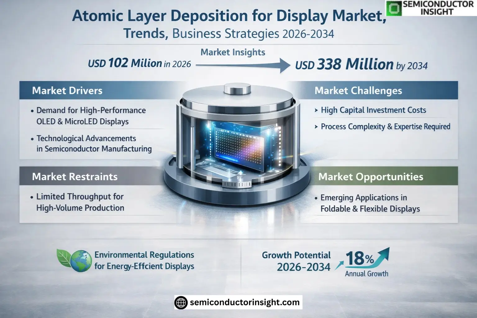
Global Atomic Layer Deposition for Display Market was valued at USD 102 million in 2026. The market is projected to grow from USD 102 million in 2026 to USD 338 million by 2034, exhibiting a CAGR of 18.2% during the forecast period.
Atomic Layer Deposition for Display (Display-ALD) refers to the application of atomic layer deposition technology in display panel manufacturing, enabling precise nanoscale thin-film deposition on glass or flexible substrates. This process ensures atomic-level thickness control and uniformity, making it ideal for high-performance applications such as OLED encapsulation, water-oxygen barrier layers, and pixel passivation in Mini-LED and Micro-LED displays.
The market growth is driven by increasing demand for advanced display technologies, particularly flexible and foldable OLEDs, which require superior thin-film encapsulation. Additionally, the rising adoption of Mini-LED and Micro-LED displays further accelerates demand due to their stringent reliability requirements. Key players like Applied Materials, Jusung Engineering, and Oxford Instruments are actively expanding their product portfolios to cater to this growing market.
MARKET DRIVERS
Growing Demand for High-Performance Displays
Atomic Layer Deposition for Display Market is experiencing significant growth due to the rising demand for high-resolution OLED and microLED displays. ALD enables ultra-thin, uniform coatings essential for advanced display technologies used in smartphones, TVs, and wearables. Manufacturers are increasingly adopting ALD to enhance device performance and durability.
Technological Advancements in Semiconductor Manufacturing
ALD’s precise thickness control and conformal deposition capabilities make it indispensable for next-generation display panels. The technology perfectly aligns with the trend toward miniaturization and flexible displays, which require atomic-level precision. Market analysts project a 12% CAGR for ALD in displays over the next five years.
Environmental regulations promoting energy-efficient displays are further accelerating ALD adoption, as the technology reduces material waste compared to conventional deposition methods.
MARKET CHALLENGES
High Capital Investment Requirements
ALD equipment represents a significant capital expenditure, with typical systems costing between USD 1-3 million. This creates barriers to entry for smaller display manufacturers and limits rapid technology adoption across all market segments.
Other Challenges
Process Complexity
Achieving optimal results with Atomic Layer Deposition requires precise process control and operator expertise, leading to extended production cycles and higher operational costs compared to alternative deposition methods.
MARKET RESTRAINTS
Limited Throughput Compared to Alternatives
While ALD offers superior film quality, its slower deposition rates remain a constraint for high-volume display production. Many manufacturers continue to favor PVD or CVD methods for applications where ultra-thin films are not critical.
MARKET OPPORTUNITIES
Emerging Applications in Foldable and Flexible Displays
The rapid development of foldable smartphone displays creates new growth opportunities for Atomic Layer Deposition technology. ALD’s ability to deposit uniform coatings on flexible substrates makes it ideal for these innovative form factors, with the market expected to grow 18% annually.
Atomic Layer Deposition for Display Market Trends
Growing Adoption in OLED and Flexible Display Manufacturing
Atomic Layer Deposition for Display Market is witnessing accelerated adoption in OLED and flexible display production, driven by its unparalleled precision in thin-film encapsulation. With OLED panel manufacturers demanding superior water and oxygen barrier performance, ALD technology provides <1nm thickness control – critical for foldable and rollable display longevity. Recent advancements in spatial ALD systems now enable deposition speeds exceeding 1000mm/sec on Gen 6 substrates, addressing throughput challenges in mass production.
Other Trends
Mini-LED/Micro-LED Process Optimization
Display ALD systems are being increasingly deployed for pixel-level passivation in next-generation Mini-LED and Micro-LED displays. The technology’s conformal coating capability ensures uniform dielectric layers across micron-scale LED structures, improving luminance efficiency by 15-20% compared to PVD alternatives. Equipment vendors are developing hybrid thermal-PEALD solutions to handle diverse material requirements from nitride encapsulation to oxide interlayers.
Asian Market Expansion and Localized Supply Chains
Over 85% of new ALD equipment installations are concentrated in Asia, mirroring the region’s display manufacturing dominance. Chinese suppliers like Qingdao Sirui now offer localized ALD solutions with 30% cost advantages over imported systems, while maintaining <0.5% particle defect rates. This localization trend extends to precursor materials, with specialized chemical suppliers establishing production bases near major panel fabs.
Multi-functional Layer Integration
Leading display manufacturers are expanding ALD applications beyond encapsulation to incorporate gate dielectrics, interfacial layers, and optical coatings in unified process flows. This integrated approach reduces manufacturing steps while improving device performance consistency. Equipment makers are responding with modular ALD platforms supporting up to 6 different material types in single deposition chambers.
Technology Convergence in Display Manufacturing
The industry is witnessing increased convergence between ALD and other deposition technologies, particularly in hybrid CVD-ALD systems for large-area displays. New co-deposition techniques combine ALD’s precision with CVD’s throughput, achieving 50% faster cycle times for TFT array applications. This technological synthesis is particularly impactful for Gen 8+ panel production where throughput and uniformity are paramount.
COMPETITIVE LANDSCAPE
Key Industry Players
Global ALD for Display Market Dominated by Specialized Equipment Providers and Material Innovators
Atomic Layer Deposition for Display Market is led by specialized equipment manufacturers with strong technological capabilities in precision deposition systems. Applied Materials, Jusung Engineering, and Oxford Instruments currently hold significant market shares, collectively accounting for over 45% of global ALD equipment supply for display applications. These companies have developed proprietary thermal ALD and plasma-enhanced ALD (PE-ALD) systems optimized for large-area glass substrates and flexible OLED production. The market exhibits a moderately concentrated structure, with the top 5 players controlling approximately 65% of installations as of 2026.
Emerging Chinese manufacturers such as Qingdao Sirui and Jiangsu Leadmicro are gaining traction through cost-competitive solutions and localized service networks, particularly in Asia’s expanding display production clusters. Niche technology providers like NCD and Optorun Semiconductor have developed spatial ALD systems specifically for Micro-LED mass transfer applications, while Skytech Inc leads in nitride ALD solutions for advanced encapsulation layers. The market continues to see strategic collaborations between ALD equipment makers and display panel manufacturers to co-develop next-generation deposition processes.
List of Key Atomic Layer Deposition for Display Companies Profiled
- Applied Materials
- Jusung Engineering
- Oxford Instruments
- Qingdao Sirui Intelligent Technology
- Jiangsu Leadmicro Nano Technology
- XIAMEN YUNMAO
- Skytech Inc
- NCD
- Optorun Semiconductor Technology
- ASM International
- Veeco Instruments
- Beneq
- Picosun
- Kurt J. Lesker Company
- CN1 (China National Optoelectronics)
Segment Analysis:
| Segment Category | Sub-Segments | Key Insights |
| By Type |
|
Production ALD Equipment is the leading segment due to:
|
| By Application |
|
OLED dominates the application segment because:
|
| By End User |
|
Smartphone Manufacturers lead end user adoption due to:
|
| By Technology |
|
Spatial ALD System is emerging as the preferred technology because:
|
| By Material |
|
Oxide ALD represents the dominant material segment through:
|
Regional Analysis: Atomic Layer Deposition for Display Market
South Korea maintains technological leadership with companies like Samsung investing heavily in ALD for quantum dot displays. The country’s focus on premium display technologies creates strong demand for atomic-level precision coating solutions.
China’s massive display production capacity drives the highest volume adoption of ALD equipment. Chinese manufacturers are rapidly transitioning from PVD to ALD methods to improve yield and reduce material consumption in display production.
Japanese chemical companies lead in developing specialized ALD precursors for display applications. Their expertise enables precise control over thin film properties critical for high-end display performance metrics.
Regional governments actively fund ALD research through public-private partnerships. South Korea’s display technology roadmap specifically identifies atomic layer deposition as a strategic technology for maintaining global competitiveness.
North America
North America shows strong growth in atomic layer deposition for display applications, particularly in advanced R&D and niche high-performance display segments. The region benefits from close collaboration between display technology developers and semiconductor equipment manufacturers adapting ALD solutions. Several startups are developing novel ALD applications for microdisplays used in AR/VR devices. U.S. research institutions continue to pioneer new ALD chemistries specifically optimized for emerging display technologies, creating a pipeline of innovations that may eventually transition to mass production.
Europe
Europe maintains a strong position in atomic layer deposition equipment manufacturing and process development for display applications. German and Finnish companies lead in producing high-precision ALD systems that meet the stringent requirements of premium display manufacturers. The region shows particular strength in developing environmentally friendly ALD processes that reduce hazardous material usage. European research institutes are focusing on roll-to-roll ALD solutions that could enable cost-effective production of large-area flexible displays in the future.
Middle East & Africa
The MEA region is witnessing growing interest in atomic layer deposition technology as local governments invest in display manufacturing capabilities. While still a developing market, strategic partnerships with Asian and European ALD equipment suppliers are helping regional manufacturers adopt the technology. The focus is primarily on ALD applications for large format displays and digital signage applications, with several pilot projects demonstrating the technology’s potential in the region’s growing consumer electronics market.
South America
South America shows emerging potential in the atomic layer deposition for display market, primarily driven by increasing local assembly of consumer electronics. Brazilian and Mexican display manufacturers are beginning to evaluate ALD solutions for improving product quality and adding value to their offerings. The region benefits from proximity to North American technology partners while developing its own ecosystem for display component manufacturing.
Report Scope
This market research report provides a comprehensive analysis of the Atomic Layer Deposition for Display Market, covering the forecast period 2026–2034. It offers detailed insights into market dynamics, technological advancements, competitive landscape, and key trends shaping the industry.
Key focus areas of the report include:
- Market Overview: The report begins with an overview outlining its current market scenario, key growth indicators, and industry transformation drivers. It discusses macroeconomic factors, demand–supply balance, regulatory landscape, and the strategic role of semiconductors in powering advancements across industries such as automotive, telecommunications, consumer electronics, and industrial automation.
- Market Size & Forecast: Historical data and future projections for revenue, unit shipments, and market value across major regions and segments.
- Segmentation Analysis: Detailed breakdown by product type, technology, application, and end-user industry to identify high-growth segments and investment opportunities.
- Regional Insights: Insights into market performance across North America, Europe, Asia-Pacific, Latin America, and the Middle East & Africa, including country-level analysis where relevant.
- Competitive Landscape: Profiles of leading market participants, including their product offerings, R&D focus, manufacturing capacity, pricing strategies, and recent developments such as mergers, acquisitions, and partnerships.
- Technology Trends & Innovation: Assessment of emerging technologies, integration of AI/IoT, semiconductor design trends, fabrication techniques, and evolving industry standards.
- Market Drivers & Restraints: Evaluation of factors driving market growth along with challenges, supply chain constraints, regulatory issues, and market-entry barriers.
- Stakeholder Insights: Insights for component suppliers, OEMs, system integrators, investors, and policymakers regarding the evolving ecosystem and strategic opportunities.
Primary and secondary research methods are employed, including interviews with industry experts, data from verified sources, and real-time market intelligence to ensure the accuracy and reliability of the insights presented.
FREQUENTLY ASKED QUESTIONS:
What is the current market size of Atomic Layer Deposition for Display Market?
-> Atomic Layer Deposition for Display Market was valued at USD 102 million in 2026. The market is projected to grow from USD 102 million in 2026 to USD 338 million by 2034, exhibiting a CAGR of 18.2% during the forecast period.
Which key companies operate in Atomic Layer Deposition for Display Market?
-> Key players include Qingdao Sirui Intelligent Technology Co., Ltd, Jusung Engineering, Applied Materials, CN1, Jiangsu Leadmicro Nano Technology Co., Ltd, XIAMEN YUNMAO, Skytech Inc, Oxford Instruments, NCD, and Optorun Semiconductor Technology, among others.
What are the key growth drivers?
-> Key growth drivers include expansion of OLED and flexible/ foldable displays, industrialization of Mini-LED/Micro-LED technologies, and increasing demand for high-performance thin-film encapsulation in display manufacturing.
Which region dominates the market?
-> Asia is the dominant market, with China, Japan, and South Korea leading production capacity and consumption due to concentrated display manufacturing facilities.
What are the emerging trends?
-> Emerging trends include advancements in spatial ALD systems, increased application in flexible display technologies, and development of high-performance barrier layers for next-generation displays.
Get Sample Report PDF for Exclusive Insights
Report Sample Includes
- Table of Contents
- List of Tables & Figures
- Charts, Research Methodology, and more...