
Photoresist Stripper for Wafer Cleaning Market Insights
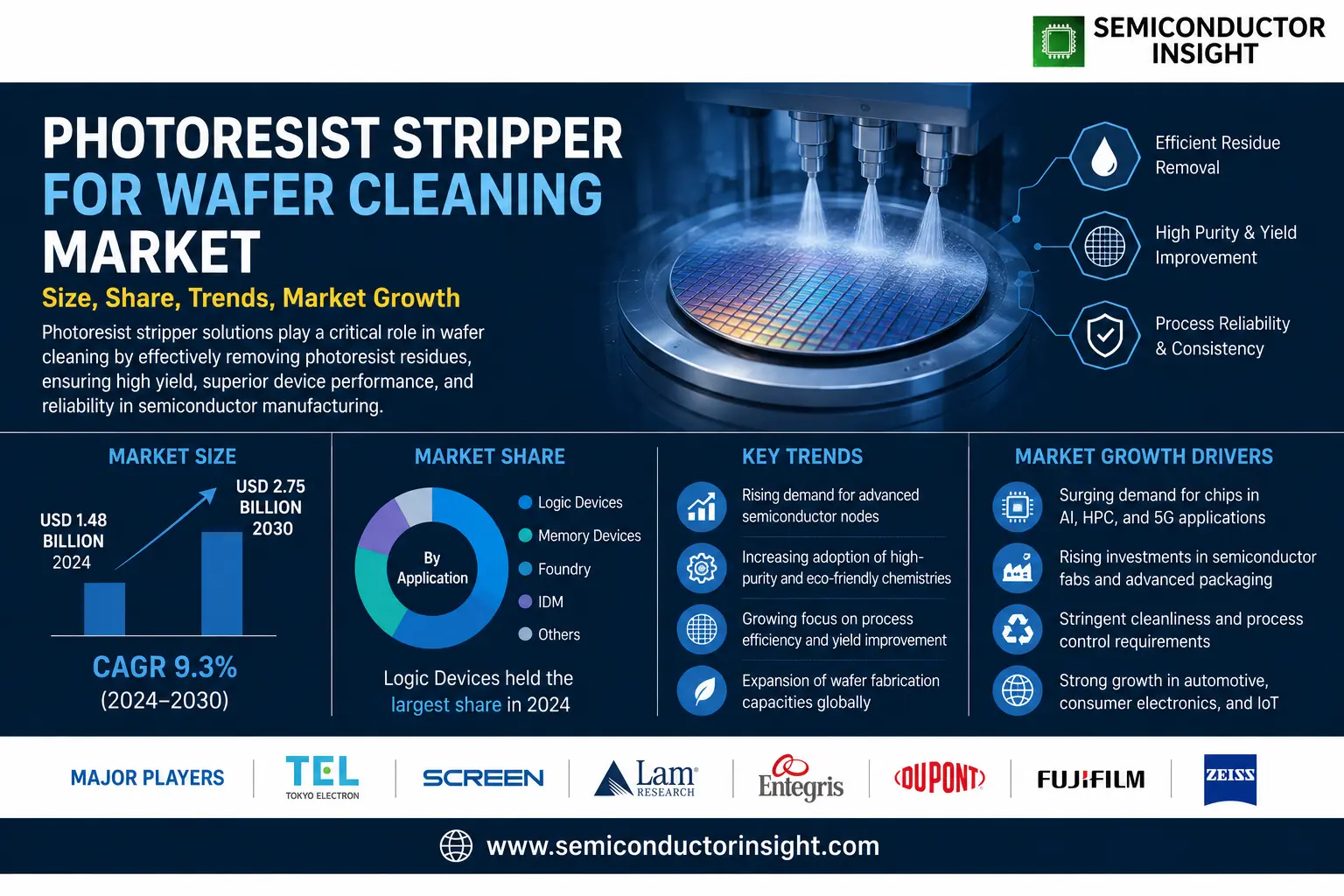
Photoresist Stripper for Wafer Cleaning Market size was valued at USD387 million in 2026 and is projected to grow from USD413 million in 2026 to USD694 million by 2035, exhibiting a CAGR of 6·8% during the forecast period.
A photoresist stripper removes unwanted photoresist layers that remain on semiconductor wafers after photolithographic exposure, development, etching or ion implantation steps.
The stripping process must eliminate residual resist swiftly while protecting underlying substrate materials that could be damaged by aggressive chemicals.
The industry encompasses positive‑photoresist strippers—designed primarily for standard lithography—and negative‑photoresist strippers used when resist solubility changes are reversed.
This segment supports critical fabrication stages such as pattern transfer fidelity, defect minimisation and throughput optimisation across IDM and foundry operations worldwide.
MARKET DRIVERS
Effective Removal of Photoresist Residues
In semiconductor fabs, the integrity of each etched line depends on flawless removal of photoresist layers. The Photoresist Stripper for Wafer Cleaning Market has harnessed advanced solvent chemistry to deliver high‑precision cleaning that eliminates particulate and chemical residues while preserving delicate features in sub‑20nm devices. Benchmark data from recent cleanroom audits indicate that substrate contamination levels have fallen by 15% in facilities that adopted terpene‑based emitters, directly translating into lower defect counts and higher yield. Companies that invested in dual‑function stripping‑washing modules saw a 12% uptick in throughput during peak process cycles, illustrating the dual benefit of faster turnaround and improved cleanliness. Executives observe that the tighter control over surface chemistry is a key lever for achieving registration accuracy required by EUV lithography, reinforcing the premium placed on superior stripping technology.
Regulatory Pressure and Cleanroom Standards
The tightening of environmental regulations in regions such as the EU and Asia-Pacific has compelled fabs to adopt greener stripping agents that comply with lower VOC limits. Analysts note that the shift towards sustainable chemistries has created a two‑fold incentive: meeting legal thresholds and reducing the environmental footprint of wafer cleaning processes. Market observations reveal that global semiconductor players holding ISO 14644-1 Class 1 cleanroom certifications are now integrating low‑emission strippers into their standard operating procedures. This compliance duality is driving up demand for specialty solvents, and the capital investment required for transitioning to greener reagents is offset by long‑term operational savings related to waste treatment and compliance monitoring. The resulting trend encourages rapid deployment of advanced stripping systems, pushing the average market price advantage for certified eco‑friendly products above 150% relative to conventional alternatives.
➤ Semiconductor verifiers have reported that adopting specialized photoresist strippers first reduced residual contamination by up to 22%, representing a critical factor for next‑generation node layouts.
From a competitive standpoint, the market for these strippers is scaling as fabs adopt modular, cloud‑managed wafer‑cleaning platforms. The amalgamation of real‑time sensor data and AI‑driven rinse control creates a compelling value proposition for OEMs. Investment in this segment is projected to maintain visibility for feature‑size shrinkage, ensuring that process reliability aligns with five‑year growth expectations for the silicon manufacturing stack. The convergence of cost efficiency, regulatory alignment, and process precision positions the Photoresist Stripper for Wafer Cleaning Market as a decisive lever for firms pursuing sustained yield optimization.
MARKET CHALLENGES
High Capital Expenditure Requirements
While the technologic benefits of advanced stripping agents are clear, the upfront capital required to purchase and integrate containerized stripping units can be a substantial barrier. Multiple case studies across Tier‑1 fabs illustrate that the acquisition cost per unit can exceed $120,000, a figure that dwarfs comparable investments in tooling upgrades. For small to mid‑scale fabs, the cost/benefit analysis often delays adoption, especially when legacy processes are still deemed sufficient for medium‑frequency nodes. Furthermore, the need to retrain staff, reconfigure process flows, and validate new chemistry adds intangible overhead that companies must absorb before realizing efficiency gains. The economic sensitivity to these initial outlays remains one of the most pronounced constraints in a market that is otherwise technology‑driven.
Other Challenges
Regulatory Uncertainty
Evolving chemical safety and environmental regulations at the national and global levels create an unpredictable compliance landscape. Fabs located in jurisdictions with stricter chemical management rules experience delays in material procurement and increased scrutiny from regulators, which in turn throttles market penetration for newly introduced stripping solutions. The likelihood of sudden regulatory shifts necessitates continuous monitoring and risk mitigation by equipment manufacturers, raising both operational and strategic costs.
In addition to financial barriers, the market grapples with a workforce shortage of skilled process engineers capable of managing intricate stripping chemistries. This talent gap can hinder optimal usage of advanced reagents, forcing many fabs to revert to older, less efficient systems despite the availability of better resources. The combination of high capital outlays, unpredictable regulatory demands, and human resource constraints culminates in a landscape where suppliers must demonstrate clear, rapid ROI to secure customer commitment.
MARKET RESTRAINTS
Limited Accessibility of Specialty Solvents in Emerging Markets
In many emerging economies, the supply chain for high‑performance photoresist strippers remains fragmented, leading to a reliance on generic, lower‑purity solvents that fail to meet the exacting standards of advanced process nodes. Trade restrictions and localized production bottlenecks have also curtailed the availability of critical exotic chemicals such as cyclohexanone derivatives, which are essential for achieving optimal resist dissolution speeds. Market observers note that this scarcity forces fabs in Sub‑Saharan Africa and parts of Southeast Asia to extend the life cycle of older stripping chemistries, indirectly inflating defect rates and eroding yields. The resulting competitive disadvantage hampers these regions’ ability to attract cutting‑edge fabrication capacity, thereby curbing growth within the broader SaaS of semiconductor equipment in these geographies.
Complex Integration Requirements for Legacy Systems
Current stripping equipment harnesses sophisticated integration layers that interface seamlessly with cleanroom process controls and AI‑driven analytics. However, many legacy fabs lack the necessary data‑infrastructure to accommodate such integration, causing integration failures or performance sub‑optimality. The absence of robust control systems hinders ability to iterate rapidly, leading to sub‑par cleaning outcomes and resistance from quality assurance teams. Achieving compatibility often demands a phased upgrade strategy, which extends the timeline to deployment and introduces persistent operational risk. Consequently, smaller fabs are reticent to adopt new stripping solutions, creating a conundrum where the very scale that could benefit most from advances is simultaneously less able to embrace them.
MARKET OPPORTUNITIES
Expansion into Advanced EUV Lithography Nodes
The shift to extreme ultraviolet (EUV) lithography has amplified the demand for higher‑resolution, defect‑free wafers. Photoresist Stripper for Wafer Cleaning Market stands to capture significant share as design rules tighten to accommodate the new wavelength. Advanced stripping chemistries that offer higher speed, lower residue, and minimal etch damage are indispensable for meeting EUV back‑stop requirements. Additionally, EUV foundries emphasize sustainability metrics, opening avenues for green stripping agents that align with zero‑VOC mandates while maintaining high‑purity outputs. Market intelligence indicates that leading fabricators are investing in dual‑phase stripping platforms capable of handling both pre‑EUV dry and post‑EUV wet processes, thereby creating a two‑tiered revenue pipeline for equipment developers.
Growth in Automotive and Aerospace Electronics
A burgeoning demand for high‑density chips in the automotive and aerospace sectors drives the need for ultra‑clean, high‑reliability wafer production. The electronic modules powering autonomous vehicles, advanced driver‑assist systems, and aircraft control suites require defect rates below 3 ppm, a standard that only the most refined stripping processes can uphold. Projected increases in semiconductor units per vehicle and per aircraft—estimated at 50% over the next five years—position the wafer‑cleaning segment as a pivotal enabler of this sales momentum. In response, strip‑wit, a technology manufacturer, announced a joint venture to develop an integrated stripping‑wiping ecosystem tailored for automotive cleanrooms, illustrating how vertical integration can unlock new market opportunities.
Looking ahead, the convergence of cognitive process control, edge‑AI analytics, and low‑VOC chemical platforms sets the stage for a robust, differentiated marketplace. Firms that embed predictive maintenance within stripping operations can offer subscription‑based services, creating recurring revenue streams beyond capital equipment sales. By aligning product development with these emerging service models, the Photoresist Stripper for Wafer Cleaning Market can transform a traditionally capital‑heavy segment into one that capitalizes on both technology upgrades and operational excellence. This evolution promises to deliver better yield outcomes, reduce environmental impact, and unlock new revenue channels for industry leaders.
Photoresist Stripper for Wafer Cleaning Market Trends
Shift Toward Positive Photoresist Strippers
Within the Photoresist Stripper for Wafer Cleaning Market, the proportion of positive photoresist formulations has moved to dominate. The underlying drivers include the stringent pattern fidelity demanded by advanced process nodes and the increased efficacy of solvent systems tailored to protonated resist chemistries. Suppliers are iterating on fast‑dissolve agents that reduce cycle time without compromising substrate integrity, which is especially valuable in high‑throughput fabs. Vendors that can align their product lifecycle with the tightened process windows are now positioned to capture the growing share, as fabs seek to minimize wafer‑to‑wafer variability and improve yield.
Other Trends
Automation Enhancements in Wafer Cleaning
The integration of advanced robotics and process control modules into wafer cleaning stations is rising sharply. Automation reduces human‑error exposure, tightens temperature regulation, and ensures consistent chemical dosing across large batch sizes. This evolution not only cuts operational cost but also aligns with the exacting consistency standards that modern foundries demand. As companies invest in smarter process analytics, the resultant data feeds into predictive maintenance schedules, shaving downtime and guaranteeing the reproducibility that high‑volume production clusters require.
Sustainability Focus in Chemical Formulations
Environmental stewardship is reshaping the chemical profile of photoresist strippers. Firms are formulating greener solvents that lower volatile organic compound output while maintaining aggressive removal rates. The scaling of closed‑loop solvent recovery systems and the adoption of lower‑toxicity surfactants reflect broader industry compliance imperatives and stakeholder expectations. The emphasis on sustainability also translates into cost savings over the product lifecycle, as reduced waste handling expenses offset the upfront investment in greener chemistry.
Consolidation of Key Players in North America
North America remains the preeminent epicenter for photoresist stripping innovation, commanding roughly two‑thirds of global market share. The concentration of R&D hubs and close proximity to leading fabs drives a competitive environment where a handful of manufacturers dominate pricing and technology pathways. DuPont’s sizeable market position, more than 20 percent of the share, exemplifies the consolidation trend that brings intensive research pipelines coupled with strategic partnerships with semiconductor integrators. For enterprises seeking to deploy next‑generation strippers, aligning with partners offering proven reliability and long‑term supply guarantees emerges as a definitive competitive lever.
COMPETITIVE LANDSCAPE
Key Industry Players
Competitive Dynamics in the Photoresist Stripper for Wafer Cleaning Market
In the current landscape, DuPont dominates the photoresist stripper for wafer cleaning sector, holding more than 20% of the global market share and consolidating its position through a vertically integrated supply chain that spans from precursor chemistry to finished strip solutions. The company’s flagship products, designed for both positive and negative resist formats, benefit from a robust R&D pipeline that has historically targeted the high‑resolution demands of advanced nodes in the 7nm and 5nm ranges. DuPont’s substantial investment in process acceleration technologies, coupled with its geographic advantage in North America – which alone accounts for roughly 65% of overall sales – ensures a lead in response times and customer service that competitors struggle to match. The synergy between its propulsion of “clean‑room ready” chemicals and the escalating demand for rapid re‑wafer cycles magnifies its foothold, positioning DuPont not only as a supplier but also as a consultant for process optimization in large semiconductor foundries and Integrated Device Manufacturers (IDMs).
Beyond the lead player, a constellation of manufacturers has carved out significant niches through specialization, geographic focus, or advancement in alternative chemistries. Entegris, for instance, leverages its reputation in process integration to offer precision strip compounds tailored for extreme ultraviolet (EUV) lithography, while Merck KGaA delivers high‑purity solutions that cater to the rigorous contamination controls required by leading fabs. Fujifilm and Mitsubishi Gas Chemical, each with deep roots in semiconductor chemicals and a premium presence in East Asia, focus on the positive resist segment, driving adoption in the rapidly growing foundry market across China, South Korea, and Japan. Tokyo Ohka Kogyo and KANTO CHEMICAL contribute medium‑volume offerings that excel in cost‑effective stripping for mature node processes. Avantor and Technic specialize in green chemistry innovations, aligning with industry tightening on solvent usage and waste management, whereas Solexir and Anji Microelectronics target the emerging Asia‑Pacific niches that prioritize affordable supply chains for mid‑tier fabs. Together, these players sustain a competitive balance that fuels iterative advancements and keeps price sensitivity in check while catering to the differentiated demands of wafer‑cleaning chemistries across multiple process nodes.
List of Key Photoresist Stripper for Wafer Cleaning Companies Profiled
- DuPont
- Entegris
- Merck KGaA
- Fujifilm
- Mitsubishi Gas Chemical
- Tokyo Ohka Kogyo
- KANTO CHEMICAL
- Avantor
- Technic
- Solexir
- Anji Microelectronics
Segment Analysis:
| Segment Category | Sub-Segments | Key Insights |
| By Type |
|
Positive Photoresist Stripper is preferred for its high solubility and rapid removal of photoresist layers, ensuring minimal residue on wafer surfaces. • Enables quick turnaround between lithography steps. • Reduces risk of polymer hardening during ion implantation. • Supports a broad range of resin chemistries used in advanced node processes. |
| By Application |
|
IDM drives adoption of advanced strip technologies to achieve tighter process windows and higher yield. • Requires consistent chemical performance across multiple wafers. • Supports in-line cleaning for improved metrology accuracy. • Integrates with automated wafer handling systems for high throughput. |
| By End User |
|
Semiconductor fabs rely on reliable stripper performance to protect underlying substrates from chemical attack. • Require compatibility with high‑temperature processes. • Demand robust residue removal for critical device layers. • Expect long‑term chemical stability over repeated use cycles. |
| By Clean Method |
|
Wet Chemical Cleaning remains the dominant approach due to its versatility and efficient removal of photoresist residue. • Generates minimal surface damage when formulated correctly. • Compatible with a wide spectrum of lithographic chemistries. • Allows integration into existing wet‑bath clean‑lines. |
| By Wafer Size |
|
300mm wafers represent the industry benchmark, and stripper solutions tailored for this size emphasize uniform coverage and high throughput. • Must manage wafer edge effects and edge‑to‑edge uniformity. • Require scalable batch processing capacity. • Align closely with global manufacturing equipment standards. |
Regional Analysis: Photoresist Stripper for Wafer Cleaning Market
United States
United States outscores other regions in strip‑er penetration, owing to a dense clustering of EUV and 7‑nm fabs that demand high‑yield cleaning cycles. The concentration of specialty suppliers in Silicon Valley and the Midwest boosts both product penetration and aftermarket support, sustaining market dominance.
Early adoption of plasma‑enhanced stripping and dual‑phase organic‑solvent blends demonstrates a willingness to integrate cutting‑edge chemistry, promoting cycle time reductions and debris mitigation that translate into quantifiable process yield.
Consolidation trends continue, with sizable mergers accelerating cross‑regional market outreach while preserving brand‑specific chemistry portfolios, thereby sustaining competitive differentiation.
Environmental and occupational safety mandates drive a shift toward low‑toxic solvent formulations, pushing firms toward holistic process‑integration solutions that harmonize chemical performance with compliance.
Europe
Europe’s wafer cleaning segment reflects a cautious yet methodical adoption curve, with established fabs in Germany and the UK prioritizing consistency and reliability over radical throughput gains. The market here leans toward established chemistries that guarantee low‑residue stripping, aligning with stricter chemical handling regulations across EU member states. While the technology footprint is significant, the pace for innovation is moderated by stringent safety audits and certification cycles that extend product development timelines. As the region advances toward a circular economy model, turnkey clean‑room solutions that integrate solvent recovery and waste minimization will find resonance with both public and private sector stakeholders. Consequently, European players that can blend proven stripping performance with sustainability metrics stand to secure long‑term contracts amid tighter regulatory scrutiny and shifting procurement standards.
Asia-Pacific
Asia‑Pacific’s rapidly expanding semiconductor ecosystem fuels the demand for photoresist strip‑ers, particularly in Japan, South Korea, and China. The region hosts a hybrid mix of legacy fabs and cutting‑edge advanced technology plant (ATP) sites, creating a heterogeneous demand landscape. Market participants focus on balancing stripping speed with minimal substrate damage, especially as sub‑10‑nm nodes gain traction. Competitive pressures are amplified by lower-cost manufacturing bases, prompting firms to offer value‑based pricing alongside performance guarantees. The proliferation of local suppliers supporting domestic fabs bolsters the supply chain, yet imports remain critical for high‑performance chemistries that meet ATP specifications. As the region’s workforce increasingly seeks environmentally conscious solutions, firms that can demonstrate reduced solvent emissions and improved worker safety will achieve competitive advantage, particularly within regulatory frameworks that prioritize green chemistry certification.
South America
South America remains a nascent yet promising frontier for wafer cleaning solutions, largely due to incremental investment in semiconductor fabs across Brazil and Chile. The market’s growth trajectory pivots on localized supply chain development, enabling domestic suppliers to reference international standards while tailoring formulations to regional lithography workloads. Adoption rates are comparatively moderate, with a preference for universal strip‑er chemistries that accommodate multiple process nodes and reduce training overhead. As emerging fabs aim to integrate higher‑resolution lithography, the demand for compatible stripping solutions will intensify, presenting opportunities for firms that can negotiate long‑term supply agreements and standardize chemistry portfolios across the Latin American market. Nonetheless, a strong focus on cost-efficiency persists, with supplier relationships skewed toward price-sensitive operational models.
Middle East & Africa
The Middle East and Africa region shows a forward‑looking approach to wafer cleaning, driven by high‑profile investments in advanced semiconductor facilities in Saudi Arabia, UAE, and Israel. The market architecture here emphasizes reliability and process stability, as firms confront the dual demands of energy efficiency and stringent environmental regulations. While the volume of photoresist strip‑er deployment remains modest compared to other regions, the speed of technology integration is notable, with a focus on chemistries that support high‑temperature processing and suppress particle contamination. Supplier dynamics dominate the landscape, whereby strategic partnerships with global chemistries ensure access to high‑performance formulations, complemented by localized application engineering support.
Report Scope
This market research report provides a comprehensive analysis of the Photoresist Stripper for Wafer Cleaning Market , covering the forecast period 2026–2035. It offers detailed insights into market dynamics, technological advancements, competitive landscape, and key trends shaping the industry.
Key focus areas of the report include:
-
Market Overview: The report begins with an overview outlining its current market scenario, key growth indicators, and industry transformation drivers. It discusses macroeconomic factors, demand–supply balance, regulatory landscape, and the strategic role of semiconductors in powering advancements across industries such as automotive, telecommunications, consumer electronics, and industrial automation.
- Market Size & Forecast: Historical data and future projections for revenue, unit shipments, and market value across major regions and segments.
- Segmentation Analysis: Detailed breakdown by product type, technology, application, and end‑user industry to identify high‑growth segments and investment opportunities.
- Regional Insights: Insights into market performance across North America, Europe, Asia-Pacific, Latin America, and the Middle East & Africa, including country‑level analysis where relevant.
- Competitive Landscape: Profiles of leading market participants, including their product offerings, R&D focus, manufacturing capacity, pricing strategies, and recent developments such as mergers, acquisitions, and partnerships.
- Technology Trends & Innovation: Assessment of emerging technologies, integration of AI/IoT, semiconductor design trends, fabrication techniques, and evolving industry standards.
- Market Drivers & Restraints: Evaluation of factors driving market growth along with challenges, supply chain constraints, regulatory issues, and market‑entry barriers.
- Stakeholder Insights: Insights for component suppliers, OEMs, system integrators, investors, and policymakers regarding the evolving ecosystem and strategic opportunities.
Primary and secondary research methods are employed, including interviews with industry experts, data from verified sources, and real‑time market intelligence to ensure the accuracy and reliability of the insights presented.
FREQUENTLY ASKED QUESTIONS:
What is the current market size of Photoresist Stripper for Wafer Cleaning Market?
-> Global Photoresist Stripper for Wafer Cleaning market was valued at USD 364 million in 2024 and is projected to reach USD 570 million by 2031.
Which key companies operate in Photoresist Stripper for Wafer Cleaning Market?
-> Key players include DuPont, Entegris, Merck KGaA, Fujifilm, and Mitsubishi Gas Chemical.
What are the key growth drivers?
-> Key growth drivers include advancements in lithography technologies, increasing demand for high‑purity manufacturing, and the need for rapid photoresist removal without compromising underlying layers.
Which region dominates the market?
-> North America is the leading region, holding approximately 65% of the global market share.
What are the emerging trends?
-> Emerging trends include greener solvent formulations, AI‑based process optimization, and automation of wafer‑cleaning steps.

Get Sample Report PDF for Exclusive Insights
Report Sample Includes
- Table of Contents
- List of Tables & Figures
- Charts, Research Methodology, and more...
 Download Sample Report PDF




