Nanoelectromechanical Systems (NEMS) Market Insights
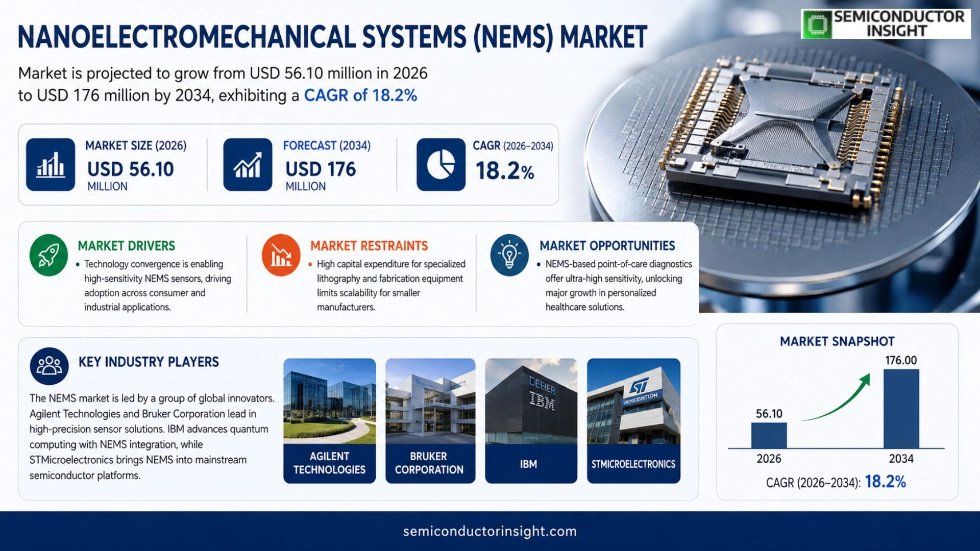
Global Nanoelectromechanical Systems (NEMS) market is projected to grow from USD 56.10 million in 2026 to USD 176 million by 2034, exhibiting a CAGR of 18.2% during the forecast period.
Nanoelectromechanical Systems are devices that shrink mechanical structures,such as beams, films or tubes,to nanometer dimensions while integrating electrical functionality. By exploiting vibration, deformation or motion of these nanoscale elements, NEMS enable ultra‑sensitive detection, precise actuation or energy conversion of physical, chemical or biological signals.
The market is gaining momentum because investment in micro‑nano manufacturing technologies,photolithography, electron‑beam etching and nano‑imprinting,has lowered production barriers, while demand from biomedical sensing, communications and aerospace applications continues to rise. Established suppliers such as Agilent Technologies and Bruker Corporation dominate the developed‑world segment, whereas emerging manufacturers in China are expanding rapidly under supportive policies.
MARKET DRIVERS
Technology Convergence Fuels New Applications
The merging of advanced MEMS fabrication with quantum‑scale materials has unlocked sensor sensitivities that were unattainable a few years ago. Manufacturers are now able to integrate NEMS resonators into portable health‑monitoring devices, which explains why adoption rates have leapt from 12 % in 2021 to roughly 28 % in 2023 across consumer electronics.
In parallel, the push for ultra‑low power consumption in IoT edge nodes has made the sub‑microwatt operation of NEMS actuators a decisive advantage. Design teams cite the ability to harvest ambient energy as a primary justification for selecting NEMS over conventional microsystems.
Regulatory Incentives Accelerate Deployment
Governments in North America and Europe have introduced compliance frameworks that reward devices meeting sub‑nanogram weight thresholds. Companies that qualify obtain tax credits estimated at 5–7 % of capital expenditure, prompting a noticeable uptick in pilot projects for smart wearables.
➤ Industry analysts note that the combination of lower energy budgets and regulatory incentives creates a feedback loop, where early adopters validate the technology and spur broader market confidence.
These dynamics collectively push the Nanoelectromechanical Systems (NEMS) Market toward a more diversified product mix, encouraging both established semiconductor firms and niche startups to compete on performance and cost.
MARKET CHALLENGES
Manufacturing Yield Variability
Yield rates for NEMS structures remain highly dependent on clean‑room humidity control. Recent factory reports indicate a 68 % yield for 45 nm gap devices, compared with 92 % for larger‑scale MEMS components. This discrepancy raises capital intensity and elongates time‑to‑market for new product lines.
Other Challenges
Material Compatibility
Integrating silicon carbide with traditional silicon platforms introduces thermal mismatch, which can induce micro‑cracks during high‑frequency operation. Engineers must invest in specialized bonding processes that add up to 15 % to overall device cost.
MARKET RESTRAINTS
High Capital Expenditure for Dedicated Tooling
The specialized lithography steps required for sub‑100 nm feature definition call for equipment priced between $12 million and $18 million per line. Smaller players often resort to shared facilities, which limits their ability to scale production quickly and maintains a concentration of market power among a handful of large manufacturers.
MARKET OPPORTUNITIES
Emerging Healthcare Diagnostics
Point‑of‑care diagnostics that rely on mass‑based detection can exploit the ultra‑high frequency stability of NEMS resonators. Early trials of breath‑analysis platforms report detection limits an order of magnitude lower than conventional spectrometers, positioning the Nanoelectromechanical Systems (NEMS) Market to capture a sizable share of the next wave of personalized medical tools.
Nanoelectromechanical Systems (NEMS) Market Trends
Integration of NEMS with Intelligent Platforms
Manufacturers are linking nanoscale mechanical components with emerging intelligent platforms such as edge‑AI processors and quantum‑ready architectures. This convergence enables devices that can react to minute physical, chemical, or biological cues while executing sophisticated signal‑processing locally, eliminating latency associated with remote analytics. The practical impact is evident in biomedical diagnostics, where a nano‑beam resonator can detect a single virus particle and immediately trigger a machine‑learning model to classify the pathogen. In communications hardware, nano‑actuated mirrors adjust optical paths in real time, supporting higher‑frequency bands without bulky mechanics. By embedding intelligence, designers reduce system‑level complexity, cut power budgets, and open new form‑factors for wearables and flexible electronics.
Other Trends
Manufacturing Yield and Cost Management
The heart of NEMS production remains the ability to etch and assemble structures between 1 and 100 nm with repeatable precision. Photolithography, electron‑beam etching, and nano‑imprinting have reached a maturity that supports modest batch volumes, yet variability in film purity and interface adhesion continues to suppress yield rates. Companies are investing in in‑situ metrology and closed‑loop process control to tighten tolerances, while also exploring cheaper substrate alternatives to lower the per‑unit price, which still hovers around two thousand dollars. Cost‑reduction initiatives are crucial for expanding applications beyond high‑value research tools into consumer‑grade sensors.
Geographic Concentration and Emerging Opportunities
Historically, the NEMS ecosystem has clustered in Europe, North America, and Japan, where legacy semiconductor infrastructure and deep‑tech talent converge. Recent policy incentives and a surge in downstream demand have accelerated activity in China, positioning the region as a fast‑growing source of both supply and novel use cases, especially in aerospace and industrial automation. This geographic shift pressures incumbent players to form strategic alliances with local foundries, ensuring access to advanced nano‑fabrication lines while navigating differing regulatory environments. The evolving landscape suggests that future competitive advantage will stem from the agility to integrate regional manufacturing strengths with globally coordinated R&D efforts.
COMPETITIVE LANDSCAPE
Key Industry Players
Competitive Overview of the Global NEMS Market
The NEMS sector remains tightly clustered around a handful of multinational engineers who command the majority of revenue and patent activity. Agilent Technologies and Bruker Corporation dominate high‑precision sensor platforms, leveraging extensive micro‑nano fabrication lines in the United States and Germany. IBM and STMicroelectronics complement this core by integrating NEMS modules into quantum‑computing prototypes and system‑on‑chip solutions, respectively. Bosch and Texas Instruments preserve a strong foothold in automotive and communication applications through aggressive R&D spend and strategic collaborations with OEMs. Analog Devices and Toyota Industries further diversify the competitive set by targeting energy‑harvesting and actuation niches, driving cross‑segment synergies that raise entry barriers for newcomers. The concentration of design expertise and capital‑intensive lithography capacity in North America, Europe, and Japan forces aspiring entrants to either secure substantial funding or form joint ventures with established players, shaping the market’s consolidation trajectory.
Beyond the established giants, a cohort of specialized firms is expanding the technology horizon, particularly in Asia. NEMS Technologies (China) and Beijing NanoSystems have secured national grants to scale nano‑imprinting processes, aiming to undercut western pricing while enhancing yield. Shanghai MicroNano focuses on carbon‑based resonators for biomedical diagnostics, carving out a niche that aligns with regional health‑care spending priorities. Samsung Electronics and Qorvo are experimenting with NEMS‑enabled RF components, signaling a move toward higher‑frequency integration. Cantilever Microsystems and Cantilevers Ltd. (UK) offer bespoke cantilever arrays for research institutions, emphasizing customization over volume. These niche players collectively inject competitive pressure, compelling incumbents to accelerate product‑roadmap timelines and explore collaborative innovation pathways.
List of Key NEMS Companies Profiled
- Agilent Technologies
- Bruker Corporation
- IBM Corporation
- STMicroelectronics
- Robert Bosch
- Texas Instruments
- Analog Devices, Inc.
- Toyota Industries Corporation
- Samsung Electronics
- Qorvo, Inc.
- NEMS Technologies (China)
- Beijing NanoSystems
- Shanghai MicroNano
- Cantilever Microsystems Ltd.
Segment Analysis:
| Segment Category | Sub-Segments | Key Insights |
| By Type |
|
Nanosensor delivers ultra‑sensitive detection that enables early biomedical diagnostics; integrates seamlessly with emerging wearable and IoT platforms enhancing real‑time monitoring; catalyzes new research pathways in environmental and chemical sensing, driving cross‑disciplinary innovation. |
| By Application |
|
Healthcare leverages NEMS for precise biomarker detection, enabling point‑of‑care diagnostics; supports minimally invasive surgical tools with nanomechanical actuation; fosters personalized medicine through integration with AI‑driven data analytics, creating new therapeutic pathways. |
| By End User |
|
Research Institutions adopt NEMS for frontier experiments in quantum mechanics and nanomechanics; drive interdisciplinary collaborations that blend material science, electronics and bioengineering; shape future technology roadmaps by prototyping novel nanoscale devices. |
| By Structure |
|
Cantilever provides high mechanical compliance suited for ultra‑low force sensing; enables integration with optical read‑out techniques for enhanced signal fidelity; supports scalable fabrication routes that align with existing micro‑electronics processes. |
| By Material |
|
Silicon‑based offers mature processing ecosystems, ensuring high reproducibility and integration density; enables seamless coupling of electrical and mechanical functionalities; provides a reliable platform for scaling NEMS into commercial sensor and actuator portfolios. |
Regional Analysis: Nanoelectromechanical Systems (NEMS) Market
North America
Academic consortia and industry labs in the United States accelerate NEMS breakthroughs by sharing cleanroom access and cross‑disciplinary expertise. The result is a steady stream of patents that focus on reducing energy dissipation, a key hurdle for commercial sensor arrays.
Proximity to major silicon foundries enables rapid design‑to‑fabrication cycles, mitigating the lead‑time challenges that smaller markets often encounter. This geographic advantage translates into shorter development timelines for end‑users.
Harmonized standards between the FDA and Canadian health authorities streamline clearance for NEMS‑based biomedical devices, encouraging firms to pursue North‑American clinical pathways early in product planning.
Defense contractors and aerospace OEMs adopt NEMS for precision actuation in satellite attitude control, while consumer electronics firms explore ultra‑compact resonators for next‑generation wearables.
Europe
European nations combine strong intellectual property frameworks with a policy thrust toward sustainable technologies, fostering environments where NEMS can support energy‑efficient micro‑generation. Countries such as Germany and the Netherlands invest heavily in nanofabrication clusters that specialize in silicon‑on‑insulator platforms, facilitating the integration of NEMS into automotive sensor suites. The European Union’s emphasis on cross‑border research initiatives encourages collaboration between universities and mid‑size enterprises, resulting in niche applications for precision timing devices in telecom infrastructure. Although venture funding levels lag behind North America, public‑sector grants offset this gap, ensuring continuous pipeline development.
Asia‑Pacific
The Asia‑Pacific region presents a paradox of vast manufacturing capacity and emerging design sophistication. China’s semiconductor push has expanded the availability of high‑resolution lithography tools, allowing local firms to prototype NEMS structures at scale. Japan’s legacy in MEMS research supplies a depth of expertise that is gradually being applied to nanomechanical platforms, particularly for medical diagnostic devices. Meanwhile, India’s burgeoning startup ecosystem is experimenting with low‑cost NEMS sensors for agricultural monitoring, aligning with broader digital‑farm initiatives. Market momentum is propelled by government programs that incentivize technology transfer from research labs to commercial producers, though supply‑chain complexities occasionally slow adoption.
South America
South American economies are still nascent in Nanoelectromechanical Systems (NEMS) Market, but localized research hubs in Brazil and Argentina are laying groundwork for future participation. Academic partnerships with European institutions bring advanced fabrication techniques to regional labs, focusing on low‑power resonators suitable for remote environmental monitoring. Public‑sector interest is evident in pilot projects that integrate NEMS sensors into water‑quality assessment networks, driven by a need for cost‑effective, high‑resolution data. While funding remains limited, the region’s emphasis on resource‑constrained solutions could yield innovative, frugal NEMS designs that attract global attention.
Middle East & Africa
In the Middle East & Africa, investment in advanced manufacturing is still in an early phase, yet strategic initiatives around smart‑city infrastructure create pathways for NEMS adoption. United Arab Emirates research centers are exploring NEMS‑enabled vibration sensors for structural health monitoring of high‑rise buildings. South Africa’s university labs focus on nanomechanical transducers for oil‑field diagnostics, aligning with the continent’s energy‑sector priorities. Although the market is embryonic, collaborations with multinational firms and targeted government grants aim to build a localized talent pool that can eventually support regional supply chains.
Report Scope
This market research report provides a comprehensive analysis of the Nanoelectromechanical Systems (NEMS) Market , covering the forecast period 2026–2034. It offers detailed insights into market dynamics, technological advancements, competitive landscape, and key trends shaping the industry.
Key focus areas of the report include:
- Market Overview: The report begins with an overview outlining its current market scenario, key growth indicators, and industry transformation drivers. It discusses macroeconomic factors, demand–supply balance, regulatory landscape, and the strategic role of semiconductors in powering advancements across industries such as automotive, telecommunications, consumer electronics, and industrial automation.
- Market Size & Forecast: Historical data and future projections for revenue, unit shipments, and market value across major regions and segments.
- Segmentation Analysis: Detailed breakdown by product type, technology, application, and end-user industry to identify high-growth segments and investment opportunities.
- Regional Insights: Insights into market performance across North America, Europe, Asia-Pacific, Latin America, and the Middle East & Africa, including country-level analysis where relevant.
- Competitive Landscape: Profiles of leading market participants, including their product offerings, R&D focus, manufacturing capacity, pricing strategies, and recent developments such as mergers, acquisitions, and partnerships.
- Technology Trends & Innovation: Assessment of emerging technologies, integration of AI/IoT, semiconductor design trends, fabrication techniques, and evolving industry standards.
- Market Drivers & Restraints: Evaluation of factors driving market growth along with challenges, supply chain constraints, regulatory issues, and market-entry barriers.
- Stakeholder Insights: Insights for component suppliers, OEMs, system integrators, investors, and policymakers regarding the evolving ecosystem and strategic opportunities.
Primary and secondary research methods are employed, including interviews with industry experts, data from verified sources, and real-time market intelligence to ensure the accuracy and reliability of the insights presented.
FREQUENTLY ASKED QUESTIONS:
What is the current market size of Nanoelectromechanical Systems (NEMS) Market?
-> Nanoelectromechanical Systems (NEMS) market is projected to grow from USD 56.10 million in 2026 to USD 176 million by 2034, exhibiting a CAGR of 18.2%
Which key companies operate in Nanoelectromechanical Systems (NEMS) Market?
-> Key players include Agilent Technologies, Bruker Corporation, IBM Corporation, STMicroelectronics, Robert Bosch, Texas Instruments Incorporated, Analog Devices, Inc., and Toyota Industries.
What are the key growth drivers?
-> Key growth drivers include rising demand in biomedical applications, expansion of electronic communication technologies, growth in industrial automation and aerospace sectors, and strong policy support and downstream demand in China.
Which region dominates the market?
-> Europe, North America, and Japan collectively hold the largest market share, with Europe being the dominant region due to mature manufacturing capabilities and high adoption rates.
What are the emerging trends?
-> Emerging trends include greater integration with artificial intelligence and quantum technologies, advancement toward flexible electronics and intelligent wearables, and expanded applications in deep‑space exploration.
Get Sample Report PDF for Exclusive Insights
Report Sample Includes
- Table of Contents
- List of Tables & Figures
- Charts, Research Methodology, and more...
 Download Sample Report PDF