Thermal Spray Coatings for Semiconductor Equipment Market Insights
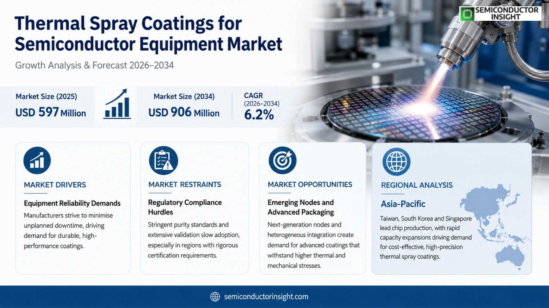
Thermal Spray Coatings for Semiconductor Equipment market was valued at USD 597 million in 2025 and is expected to increase to USD 906 million by 2034, reflecting a CAGR of 6.2 % during the forecast period.
Thermal spray coating services protect critical semiconductor‑fabrication components,such as chambers, showerheads (GDP), electrostatic chucks (ESC), liners, baffles, shield covers, heaters, shutters, focus rings, edge rings, ceramic windows and etch‑gas injectors,from the aggressive chemistries and high‑temperature cycles inherent in wafer processing. By depositing dense ceramic or metal‑alloy layers through plasma or arc spray techniques, manufacturers extend part lifetimes, reduce particle generation and maintain process stability across advanced nodes. The dominance of ceramic formulations (approximately 69 % share) reflects their superior resistance to fluorine‑rich etchants, while plasma spray remains the primary technology platform due to its scalability and cost efficiency.
MARKET DRIVERS
Equipment Reliability Demands
Thermal Spray Coatings for Semiconductor Equipment Market is gaining traction as manufacturers strive to minimise unplanned downtime. Advanced spray technologies create a protective layer that resists chemical erosion and high‑temperature cycling, directly extending tool life by an estimated 30‑40 %. This endurance translates into higher wafer‑throughput and a measurable uplift in plant‑level productivity.
Cost Efficiency Pressures
Operating margins in semiconductor fabs are tightly compressed, prompting a shift toward solutions that lower total cost of ownership. Thermal spray coatings reduce the frequency of component replacement, curbing consumable spend by up to 25 % in high‑volume lines. The resulting savings justify the upfront investment in coating services for a broad range of equipment, from lithography to etch chambers.
➤ “Adopting thermal spray protection can shave 15‑20 % off annual maintenance budgets while delivering an extra two years of service life for critical hardware.”
Beyond immediate cost benefits, the coating process aligns with sustainability goals by limiting waste generated from part scrappage. Facilities that integrate these coatings report a modest reduction in carbon intensity, reinforcing the strategic appeal of the technology in an industry that is increasingly judged on environmental performance.
MARKET CHALLENGES
Process Integration Complexity
Embedding thermal spray steps into existing production flows requires specialised tooling and skilled operators. The learning curve can delay rollout, especially for fabs that operate 24 × 7 schedules. Companies must therefore allocate dedicated engineering resources, which can strain already tight project timelines.
Other Challenges
Supply‑Chain Vulnerability
The niche nature of high‑precision spray materials means that shortages in feedstock can ripple through the coating schedule. Limited numbers of certified service providers exacerbate the risk, making contingency planning a critical element of project management.
MARKET RESTRAINTS
Regulatory Compliance Hurdles
Coatings applied to equipment that contacts silicon wafers must meet stringent purity standards. Any trace contamination can impact device yield, prompting regulators to scrutinise the composition of spray alloys. The need for extensive validation testing slows market adoption, particularly in regions with rigorous certification regimes.
MARKET OPPORTUNITIES
Emerging Nodes and Advanced Packaging
As the semiconductor industry pushes beyond 3‑nm logic nodes and embraces heterogeneous integration, equipment operates under more severe thermal and mechanical stresses. Thermal spray coatings engineered for higher temperature tolerance open a pathway to support these next‑generation processes, creating a significant revenue stream for coating vendors willing to tailor formulations to the new specifications.
Thermal Spray Coatings for Semiconductor Equipment Market Trends
Regional Growth Propelled by Fab Expansion
The latest revenue figures show the North American segment climbing from $220.58 million in 2024 to an estimated $326.14 million by 2031, while Asia‑Pacific is set to outpace its peers, moving from $407.53 million to $674.74 million over the same horizon. Europe, though smaller, follows a steady path from $66.62 million to $91.83 million. These trajectories mirror the broader acceleration in semiconductor fab investment, especially in advanced logic and memory nodes where higher‑temperature etch and deposition tools demand more frequent recoating. The correlation between equipment capital spend and the need for durable surface protection underpins the upward pressure on Thermal Spray Coatings for Semiconductor Equipment Market across all three regions.
Other Trends
Material Preference Shifts
Ceramic formulations continue to dominate, holding roughly 69 percent of the material mix in 2024. Yet the portfolio is diversifying as manufacturers experiment with fluorine‑rich yttrium oxy‑fluorides and complex oxide blends that promise lower particle emission under fluorine‑laden chemistries. This material evolution is not merely academic; it directly addresses contamination concerns that can erode wafer yield in sub‑10 nm processes. Suppliers that can deliver high‑purity powders at scale are gaining preferential access to fab‑proximate service hubs, a factor that increasingly differentiates market participants.
Technology Evolution and Competitive Landscape
Plasma spray remains the workhorse, accounting for about 73 percent of all coating applications in 2024 and projected to edge close to 75 percent by 2031. Nonetheless, the PVD, CVD and ALD niche is gathering momentum, propelled by the push for thinner, multilayer stacks that suppress particle shedding. The competitive field is highly consolidated: the top five players control roughly 58 percent of global revenue, while the top ten exceed 72 percent. Companies headquartered in the United States, Germany, Japan, South Korea and Taiwan dominate both the service model and the advanced coating‑technology segment. Their extensive fab‑service networks and established relationships with equipment OEMs position them to capture the bulk of incremental demand as the industry transitions toward denser, higher‑performance process flows.
COMPETITIVE LANDSCAPE
Key Industry Players
Thermal Spray Coatings for Semiconductor Equipment – Competitive Outlook
The market is markedly concentrated, with the five largest firms accounting for roughly 58 % of global revenue in 2024. KoMiCo, Oerlikon Balzers, Entegris, Beneq and TOCALO Co., Ltd. command this share through vertically integrated operations that span high‑purity powder production, plasma‑spray execution, and post‑process qualification. Their dominance is reinforced by the fact that plasma spray supplies more than 70 % of all applied coatings, a technology that demands rigorous control of particle emission and coating uniformity for etch and deposition tools. Clients gravitate toward these providers because they can certify coating performance across multiple process nodes, thereby reducing downtime and minimizing contamination risk. The ability to bundle service, spare‑part logistics and long‑term reliability data translates into pricing power and influences the broader supply‑chain dynamics for semiconductor manufacturers.
Beyond the top tier, a spectrum of specialist firms adds depth to the competitive arena. UCT (Ultra Clean Holdings, Inc.) leverages a North‑American service network to offer rapid turnaround for chamber components, while Pentagon Technologies differentiates itself through bespoke line‑extension programs for advanced logic fabs. Mitsubishi Chemical (Cleanpart) applies its chemical‑manufacturing heritage to develop hybrid plasma‑/CVD solutions that address emerging fluorine‑rich chemistries. Asian players such as DFtech, Ferrotec (Anhui) Technology Development, and Jiangsu Kaiweitesi Semiconductor are channeling R&D into yttrium‑based fluorides and complex oxides, aiming to replace conventional yttria in high‑fluorine etch environments. These regional actors intensify price competition and accelerate innovation cycles, compelling the global leaders to augment their service footprints and co‑development initiatives. Collectively, the expanding pool of niche suppliers raises the bar for qualification depth, powder purity, and proximity to fab clusters, shaping strategic decisions for equipment OEMs and fab managers alike.
List of Key Thermal Spray Coatings for Semiconductor Equipment Companies Profiled
- KoMiCo
- Entegris
- Oerlikon Balzers
- Beneq
- TOCALO Co., Ltd.
- UCT (Ultra Clean Holdings, Inc.)
- Pentagon Technologies
- Mitsubishi Chemical (Cleanpart)
- FM Industries
- Frontken Corporation Berhad
- Hansol IONES
- Jiangsu Kaiweitesi Semiconductor
- KERTZ HIGH TECH
- TOPWINTECH
- SilcoTek
Segment Analysis:
| Segment Category | Sub-Segments | Key Insights |
| By Type |
|
Ceramic Coating
|
| By Application |
|
Etching
|
| By End User |
|
Foundry fabs
|
| By Process Node |
|
Advanced 110 nm and below
|
| By Technology |
|
Plasma Spray
|
Regional Analysis: Thermal Spray Coatings for Semiconductor Equipment Market
North America
Major coating applicators have expanded clean‑room‑compatible lines in the Midwest and Southern California, allowing swift deployment to fabs that demand contamination‑free environments. The proximity of these facilities to leading chip manufacturers shortens logistics cycles and supports just‑in‑time maintenance contracts.
Partnerships between university labs and equipment producers focus on high‑entropy alloys and nanostructured oxides, targeting lower thermal conductivity without sacrificing hardness. Funding from federal technology programs accelerates prototype testing within state‑run pilot fabs.
Recent shortages of specialty powders prompted firms to diversify raw‑material sourcing across Canada and the United States, creating a buffer against export restrictions. Localized stockpiles are now a standard clause in service agreements.
EPA guidelines on particulate emissions and clean‑room classifications have shaped coating‑process selections. Companies that can certify compliance gain a competitive edge when bidding for high‑volume wafer production contracts.
Europe
European fabs, especially those in Germany, the Netherlands and France, are integrating thermal spray coatings to address the relentless push toward sub‑5 nm nodes. Industry consortia coordinate standards for coating thickness and adhesion, enabling cross‑border equipment sharing. While the market is more fragmented than North America, the presence of several Tier‑1 coating specialists offers a rich selection of customized formulations that meet the stringent environmental regulations prevalent across the EU.
Asia‑Pacific
In the Asia‑Pacific corridor, Taiwan, South Korea and Singapore dominate chip production, and their rapid capacity expansions have heightened demand for durable tool surfaces. Local manufacturers are leveraging cost‑effective spray techniques to keep equipment budgets manageable while still achieving the precision required for advanced lithography. The region’s emphasis on high‑volume manufacturing fuels a competitive environment where speed of coating application influences equipment turnover rates.
South America
Brazil and Chile host a growing number of specialty semiconductor assembly plants that are beginning to adopt thermal spray coatings as a means to offset limited access to high‑end replacement parts. The market here is characterized by a focus on reliability; firms prefer proven coating chemistries that can operate under the region’s diverse climatic conditions, from humid coastal zones to arid highlands.
Middle East & Africa
Emerging semiconductor test and packaging facilities in the United Arab Emirates and South Africa view thermal spray coatings as a strategic lever to enhance equipment uptime in markets where skilled maintenance personnel are scarce. Investment is concentrated on training programs that certify local technicians, ensuring that coating application and inspection can be performed without relying on overseas service crews.
Report Scope
This market research report provides a comprehensive analysis of the Thermal Spray Coatings for Semiconductor Equipment Market , covering the forecast period 2026–2034. It offers detailed insights into market dynamics, technological advancements, competitive landscape, and key trends shaping the industry.
Key focus areas of the report include:
- Market Overview: The report begins with an overview outlining its current market scenario, key growth indicators, and industry transformation drivers. It discusses macroeconomic factors, demand–supply balance, regulatory landscape, and the strategic role of semiconductors in powering advancements across industries such as automotive, telecommunications, consumer electronics, and industrial automation.
- Market Size & Forecast: Historical data and future projections for revenue, unit shipments, and market value across major regions and segments.
- Segmentation Analysis: Detailed breakdown by product type, technology, application, and end-user industry to identify high-growth segments and investment opportunities.
- Regional Insights: Insights into market performance across North America, Europe, Asia-Pacific, Latin America, and the Middle East & Africa, including country-level analysis where relevant.
- Competitive Landscape: Profiles of leading market participants, including their product offerings, R&D focus, manufacturing capacity, pricing strategies, and recent developments such as mergers, acquisitions, and partnerships.
- Technology Trends & Innovation: Assessment of emerging technologies, integration of AI/IoT, semiconductor design trends, fabrication techniques, and evolving industry standards.
- Market Drivers & Restraints: Evaluation of factors driving market growth along with challenges, supply chain constraints, regulatory issues, and market-entry barriers.
- Stakeholder Insights: Insights for component suppliers, OEMs, system integrators, investors, and policymakers regarding the evolving ecosystem and strategic opportunities.
Primary and secondary research methods are employed, including interviews with industry experts, data from verified sources, and real-time market intelligence to ensure the accuracy and reliability of the insights presented.
FREQUENTLY ASKED QUESTIONS:
What is the current market size of Thermal Spray Coatings for Semiconductor Equipment Market?
-> Thermal Spray Coatings for Semiconductor Equipment market is expected to increase to USD 906 million by 2034, reflecting a CAGR of 6.2 %
Which key companies operate in Thermal Spray Coatings for Semiconductor Equipment Market?
-> Key players include KoMiCo, Cinos, TOCALO, WONIK QnC, Beneq, Entegris, Inficon, Oerlikon Balzers, UCT (Quantum Clean), Pentagon Technologies, Enpro Industries, Mitsubishi Chemical (Cleanpart), FM Industries, and many regional specialists across the USA, Germany, Japan, South Korea, Taiwan, Singapore and China Mainland.
What are the key growth drivers?
-> Key growth drivers include the harsh abrasive environment of semiconductor fabs that shortens chamber component life, increasing demand for coating services; rising capex and AI‑driven equipment upgrades; expanding installed base of etch and deposition tools; and the need for particle‑free, high‑purity surfaces to protect yield.
Which region dominates the market?
-> Asia-Pacific dominates the market, with the region valued at USD 407.53 million in 2024 and projected to reach USD 674.74 million by 2031, supported by the highest CAGR of 7.86% among all regions.
What are the emerging trends?
-> Emerging trends include a shift toward advanced plasma‑spray formulations, accelerated growth of PVD/CVD/ALD hybrid multilayer coatings, development of fluorine‑containing yttrium (YOF/YF) systems for enhanced plasma resistance, and increasing adoption of ceramic coatings which now hold about 69.39% market share.

Get Sample Report PDF for Exclusive Insights
Report Sample Includes
- Table of Contents
- List of Tables & Figures
- Charts, Research Methodology, and more...
 Download Sample Report PDF