
Global Metal-Semiconductor-Metal Photodetector Market Insights
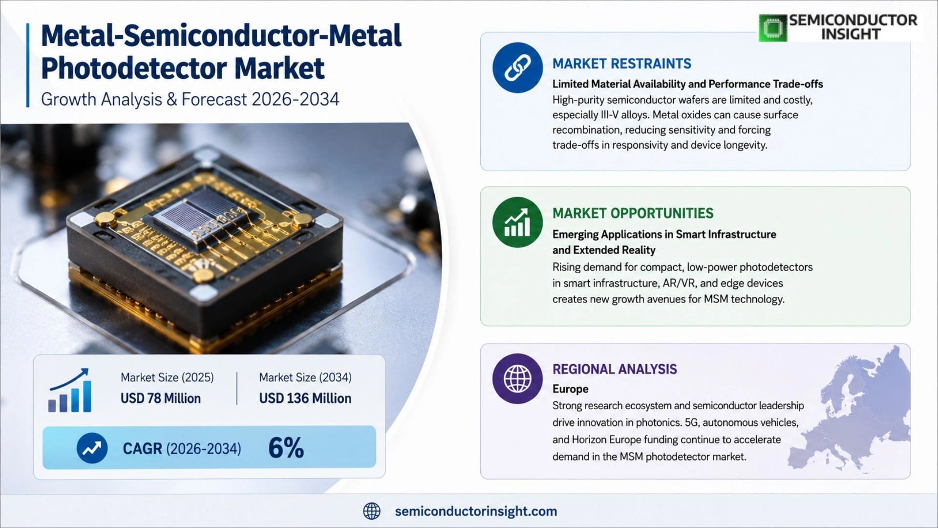
Metal-Semiconductor-Metal Photodetector market was valued at USD 78 million in 2025 and is projected to reach USD 136 million by 2034, exhibiting a compound annual growth rate of approximately 6% during the forecast period.
A metal-semiconductor-metal photodetector consists of interdigitated metal fingers fabricated on a semiconductor substrate; it converts incident photons into measurable electrical signals by collecting photoexcited electrons and holes that drift under an applied electric field between the metal electrodes.
Its compact architecture enables integration into photonic integrated circuits, supporting wavelengths ranging from visible to near-infrared.
The device’s high responsivity makes it suitable for optical fiber communication links and high-speed receivers in telecom infrastructure.
MARKET DRIVERS
Demand Surge in High‑Speed Communication Systems
In the current semiconductor ecosystem, the need for compact, low‑latency sensors has pushed adoption of Metal‑Semiconductor‑Metal Photodetector Market components in data‑center backplanes and fiber‑optic transceivers. Their intrinsic capability to convert optical signals with minimal heat dissipation aligns well with the energy‑efficiency mandates of modern networks, while their planar architecture eases integration with complementary metal‑oxide‑semiconductor processing lines.
Advancements in Sensing and Imaging Technologies
Recent breakthroughs in nanostructure engineering have delivered detectors with extended responsivity between the near‑infrared and visible bands, dramatically improving imaging fidelity for autonomous navigation and medical diagnostics. The addition of plasmonic enhancement layers further elevates signal‑to‑noise ratios, creating a compelling proposition for sectors that require precision under low‑light conditions.
➤ Integration scalability has become pivotal, as system designers increasingly target high‑throughput photonic circuits within single wafers.
Because these devices can be fabricated under standard lithographic steps and are compatible with existing packaging techniques, the barrier to mass production is eroding. This synergy with mainstream semiconductor manufacturing underscores the rapid uptake across commercial photonic integrated circuit portfolios.
MARKET CHALLENGES
Complexity of Device Fabrication at Scale
While fabrication steps appear straightforward, maintaining uniform electrical contact across the heterostructure demands meticulous control of deposition thicknesses and interface quality. Variations lead to inconsistent responsivity and increased process yield loss, driving up the total cost of ownership for manufacturers. Moreover, the delicate balance between conductivity and optical transparency poses a persistent design dilemma for engineers seeking maximal quantum efficiency.
Other Challenges
Material and Process Constraints
Substrate lattice mismatch can induce dislocation networks that degrade carrier lifetimes; high‑temperature anneals necessary for doping often compromise metal adhesion, necessitating alternative diffusion schemes or buffer layers. Packaging under vacuum or controlled atmospheres further escalates capital expenditure, limiting entry for small‑to‑medium enterprises.
MARKET RESTRAINTS
Limited Material Availability and Performance Trade‑offs
Access to high‑purity, defect‑free semiconductor wafers remains a bottleneck, especially for III‑V alloys that exhibit superior bandgap energies yet are costly to procure. The intrinsic property of metals to form native oxides can introduce surface recombination centers, effectively lowering detector sensitivity. Balancing these trade‑offs forces designers to compromise either on responsivity or longevity, which constrains the application scope of Metal‑Semiconductor‑Metal devices in battery‑powered or harsh‑environment contexts.
MARKET OPPORTUNITIES
Emerging Applications in Smart Infrastructure and Extended Reality
The shift toward connected urban ecosystems and immersive experiences is generating fresh demand for ultrathin, lightweight photodetectors capable of operating at variable wavelengths. Deployment in smart street lighting, structural health monitoring, and AR/VR displays demands detectors that combine low power draw with rapid recovery times, a criterion that the latest Metal‑Semiconductor‑Metal iterations meet. Coupled with the adoption of edge computing strategies, these devices can deliver real‑time optical sensing data without reliance on centralized servers, unlocking new revenue streams for system integrators.
Metal‑Semiconductor‑Metal Photodetector Market Trends
Rise in Integration of MSM Detectors into Optical Communication Systems
The surge in bandwidth demands from 5G networks and hyperscale data centers has intensified the need for photodetectors that offer both high speed and low latency. MSM devices, with their interdigitated metal fingers and efficient carrier collection, naturally meet these criteria. As a result, telecom and optical fiber communication segments are increasingly adopting MSM configurations, particularly those based on GaAs and InGaAs, to achieve detection limits below 1 picowatt while maintaining nanosecond‑scale response times. This shift places a premium on device architectures that balance material performance with manufacturability, prompting suppliers to refine process steps that minimize overlap between fingers and reduce surface recombination. The Metal‑Semiconductor‑Metal photodetector market finds itself positioned at the intersection of high‑throughput data needs and manufacturing scalability.
Other Trends
Adoption of Silicon‑Based Photonics
Integrating MSM detectors directly onto silicon photonic chips is converging the growth of the silicon photonics ecosystem with the rising requirement for high‑speed optical interfaces. Leveraging CMOS fabrication lines, silicon‑based MSM structures reduce not only unit cost but also packaging complexity, allowing rapid scaling to mass‑produced traffic monitoring modules. This trend also drives investment in novel doping profiles that compensate for silicon’s indirect bandgap, enabling responsivity improvements without compromising speed.
Rise of Flexible, Low‑Power MSM Solutions for IoT
Edge devices and wearables demand photodetectors that consume milliwatts while maintaining responsiveness in harsh environments. Researchers are extending the MSM concept onto flexible polyimide substrates, exploiting carbon‑nanotube or thin‑film oxide semiconductors to lower capacitance and dark current. Early pilots in industrial IoT sensing and health monitoring suggest that flexible MSM units can sustain sub‑100 µs rise times, positioning them as attractive alternatives to bulk counterparts for distributed sensor networks. The Metal‑Semiconductor‑Metal photodetector market is also testing flexible architectures that lower energy draw.
Collectively, these movement patterns suggest that capital allocation should prioritize materials that reconcile speed with cost while embracing integration pathways that align with prevailing semiconductor manufacturing capacities. Companies that invest in hybrid designs,combining high‑performance III‑V active regions with silicon back‑end processes,are likely to capture incremental market share in both high‑bandwidth telecom and expanding IoT verticals. Moreover, maintaining a balanced R&D portfolio that addresses dark‑current suppression, packaging, and long‑term reliability will be decisive for the Metal‑Semiconductor‑Metal photodetector market as it continues to meet demanding end‑use parameters.
COMPETITIVE LANDSCAPE
Key Industry Players
Metal‑Semiconductor‑Metal Photodetector Market Landscape
HAMAMATSU, with its earliest adoption of MSM technology, controls around 30% of the global SMB photodetector revenue, thanks to its heritage in high‑resolution imaging and laser diode integration. The company’s focus on GaAs‑based MSM detectors and recent expansion into mid‑IR wavelengths has positioned it as the benchmark for industrial and defense segments. In 2023, its sales surpassed US$ 93 million, reflecting a 4.5% increase over the preceding year, while its gross margin of 28% underscores efficient supply‑chain management and cost‑controlled R&D. The €55 million investment announced in 2024 to double the wafer‑level throughput in Yokohama will enable a 15% lead over competitors by 2026. Critically, the company’s vertical integration,from epitaxial growth to die‑bonding,reduces lead times and shields it from silicon‑based supply turbulence. Meanwhile, its strong presence in U.S. defense procurement cycles, coupled with an expanding footprint in European aerospace contracts, grants it a pricing advantage that constrains discounting pressure in the high‑end channel. Across the supply chain, Hamamatsu’s partnership with KLA‑Evolv for process monitoring has further compressed production costs, enabling the firm to reclaim a bigger share of the gross margin without sacrificing performance metrics critical to photonic integrated circuits. Consequently, the firm’s strategic investments in nanostructured MSM surfaces promise to unlock sub‑10‑nm feature sizes, positioning it at the frontier of next‑generation visible‑to‑IR fusion applications.
Other key providers such as OSI Laser Diode, Excelitas Technologies, Teledyne e2v, IQE plc, and Samsung Electronics carve out significant niches across specific wavelengths and application domains. OSI’s recently unveiled fiber‑integrated MSM array targets high‑speed optical communications, capturing a 12% share of the optical‑fiber segment despite operating in a highly commodified space. Excelitas has leveraged its InGaAs MSM line to penetrate the autonomous‑vehicle sensor market, achieving a 9% penetration in that sub‑segment by 2023. Teledyne e2v’s collocation with defense clients through joint‑development agreements secures long‑term revenue streams and access to cutting‑edge cryogenic MSM modules. InGaAs‑centred offerings from IQE plc and Dynamic Laser Technologies fill the spectre from telecom to deep‑space imaging, while Korean player Samsung Electronics provides cost‑competitive MSM solutions for consumer photonics. Collectively, these players illustrate an emergent cluster that balances technological leadership with geographic diversification, thereby mitigating the risk associated with single‑region concentration.
List of Key Metal‑Semiconductor‑Metal Photodetector Companies Profiled
- Hamamatsu Photonics
- OSI Laser Diode
- Excelitas Technologies
- Teledyne e2v
- IQE plc
- Dynamic Laser Technologies
- Thorlabs
- QinetiQ
- Samsung Electronics
- Semiconductor Research Institute
- Imperial Innovation Ltd
- OptoWave Electronics
- ISOF
Segment Analysis:
| Segment Category | Sub-Segments | Key Insights |
| By Type |
|
Monolithic MSM offers high responsivity and low fabrication cost. • Its simple interdigitated structure enables rapid scaling. • The lack of isolation layers reduces parasitic capacitance, improving speed. • Compatibility with standard CMOS processes eases integration into larger systems. • Manufacturers emphasize high yield through refined lithography and metal deposition techniques. |
| By Application |
|
Optical Fiber Communications relies on MSM detectors for high-bandwidth data links. • They provide fast rise times suitable for gigabit operations. • Low dark current reduces noise in long-haul links. • Their compact layout aligns with dense photonic circuits. • Continuous improvements target enhanced spectral selectivity to support wavelength-division multiplexing. |
| By End User |
|
Telecommunication Operators require robust high-speed detectors for backbone infrastructure. • They prioritize reliability and long-term support. • Devices must withstand high optical power regimes. • Design trends focus on low jitter for coherent modulation schemes. • Oxygen-free fabrication improves lifespan in fiber environments. |
| By Device Architecture |
|
Hybrid MSM-CMOS merges detector sensitivity with on-chip processing. • It enables immediate signal conditioning, reducing latency. • Integration lowers interconnect counts, enhancing power efficiency. • Designers balance trade-offs between detector speed and processing density. • Market moves toward programmable photonic front ends for flexible bandwidth allocation. |
| By Integration Level |
|
System-on-Chip integration offers end-to-end optical solutions. • It reduces assembly complexity and footprint. • Users gain predictable performance in constrained environments. • Thermal management becomes critical for high-density packaging. • Partnerships between detector and ASIC vendors accelerate time-to-market for emerging platforms. |
Regional Analysis: Metal‑Semiconductor‑Metal Photodetector Market
Europe
Europe’s research grants and cross‑border consortia lower development costs for MS‑M photodetector prototypes, enabling rapid iteration. Coupled with a robust semiconductor findry sector, this environment nurtures innovation that spills over into commercial offerings.
The market is moderately fragmented, with a handful of specialty players forming strategic alliances to pool expertise in materials science and packaging. Such coalitions accelerate footprint reduction and improve yield metrics.
The rise of integrated photonic circuits for biotech diagnostics and the expansion of retinal imaging hardware provide new application domains for high‑sensitivity MS‑M arrays.
Supply‑chain bottlenecks for crystalline silicon and rare‑earth dopants necessitate aggressive local sourcing strategies to sustain production pace.
North America
North America continues to pursue aggressive deployments of MS‑M photodetectors within aerospace and defense applications, where detection sensitivity dictates mission success. The region’s substantial venture capital ecosystem encourages early‑stage technology transfer, while a well‑established supply chain of high‑purity semiconductor substrates underpins scalable manufacturing. However, rising commodity prices and stringent export controls introduce volatility that could temper investment density. Companies that integrate computational imaging algorithms with photodetector arrays stand to capture differentiated market segments, particularly in high‑resolution optical imaging.
Asia‑Pacific
Asia‑Pacific is a critical growth engine, propelled by massive industrial automation initiatives and an expanding smart‑city infrastructure portfolio. Rapid digitization in semiconductor centers, particularly in East Asia, is setting the stage for widespread adoption of MS‑M sensors in robotics and IoT gateways. Nevertheless, regional disparities in intellectual‑property enforcement can impede technology diffusion, prompting firms to focus on local R&D hubs to guard competitive advantage. The confluence of cost‑efficient manufacturing and a robust domestic market yields a compelling value proposition for high‑performance photodetectors.
South America
South America’s emphasis on renewable‑energy installations and agricultural monitoring presents unique niches for MS‑M photodetectors capable of functioning under extreme temperature swings and low‑light conditions. While infrastructural bottlenecks limit immediate uptake, emerging public‑private partnerships in Brazil and Chile are beginning to finance pilot projects that demonstrate the technology’s resilience in harsh outdoor environments. Manufacturers with modular, HVAC‑tolerant designs are likely to dominate the regional share as deployment scales.
Middle East & Africa
The Middle East & Africa region is experiencing a rapid inflection point in digital transformation, spurred by post‑conflict reconstruction and burgeoning e‑commerce ecosystems. MS‑M photodetectors find application in secure gateway deployments and advanced imaging in security surveillance. However, limited access to high‑grade semiconductor tooling and a shortage of locally retained expert talent impose significant integration barriers. Companies that establish training programs and localized supply agreements can mitigate these constraints and unlock long‑term market footholds.
Report Scope
This market research report provides a comprehensive analysis of the Metal-Semiconductor-Metal Photodetector Market , covering the forecast period 2026–2034. It offers detailed insights into market dynamics, technological advancements, competitive landscape, and key trends shaping the industry.
Key focus areas of the report include:
- Market Overview: The report begins with an overview outlining its current market scenario, key growth indicators, and industry transformation drivers. It discusses macroeconomic factors, demand–supply balance, regulatory landscape, and the strategic role of semiconductors in powering advancements across industries such as automotive, telecommunications, consumer electronics, and industrial automation.
- Market Size & Forecast: Historical data and future projections for revenue, unit shipments, and market value across major regions and segments.
- Segmentation Analysis: Detailed breakdown by product type, technology, application, and end-user industry to identify high-growth segments and investment opportunities.
- Regional Insights: Insights into market performance across North America, Europe, Asia-Pacific, Latin America, and the Middle East & Africa, including country-level analysis where relevant.
- Competitive Landscape: Profiles of leading market participants, including their product offerings, R&D focus, manufacturing capacity, pricing strategies, and recent developments such as mergers, acquisitions, and partnerships.
- Technology Trends & Innovation: Assessment of emerging technologies, integration of AI/IoT, semiconductor design trends, fabrication techniques, and evolving industry standards.
- Market Drivers & Restraints: Evaluation of factors driving market growth along with challenges, supply chain constraints, regulatory issues, and market-entry barriers.
- Stakeholder Insights: Insights for component suppliers, OEMs, system integrators, investors, and policymakers regarding the evolving ecosystem and strategic opportunities.
Primary and secondary research methods are employed, including interviews with industry experts, data from verified sources, and real-time market intelligence to ensure the accuracy and reliability of the insights presented.
FREQUENTLY ASKED QUESTIONS:
What is the current market size of Metal-Semiconductor-Metal Photodetector Market?
-> Metal-Semiconductor-Metal Photodetector market is projected to reach USD 136 million by 2034, exhibiting a compound annual growth rate of approximately 6%
Which key companies operate in Metal-Semiconductor-Metal Photodetector Market?
-> Key players include Hamamatsu Photonics and OSI Laser Diode, among others.
What are the key growth drivers?
-> Key growth drivers include the rising demand for high-performance photodetectors in IoT-based electronics, automotive applications, and optical communication systems, as well as continuous advancements in semiconductor technology and integration with photonic circuits.
Which region dominates the market?
-> The market is highly global, with significant installations in North America and Asia-Pacific, and no single region currently dominates; however, market penetration is growing fastest in North America and China due to strong semiconductor ecosystems.
What are the emerging trends?
-> Emerging trends include the adoption of advanced material platforms such as InGaAs, integration of photonic integrated circuits, and the use of metal-semiconductor-metal photodetectors in real-time embedded processing for IoT and automotive applications.

Get Sample Report PDF for Exclusive Insights
Report Sample Includes
- Table of Contents
- List of Tables & Figures
- Charts, Research Methodology, and more...
 Download Sample Report PDF




