High Purity Semi – InsulatIng SIC Substrate Market Insights
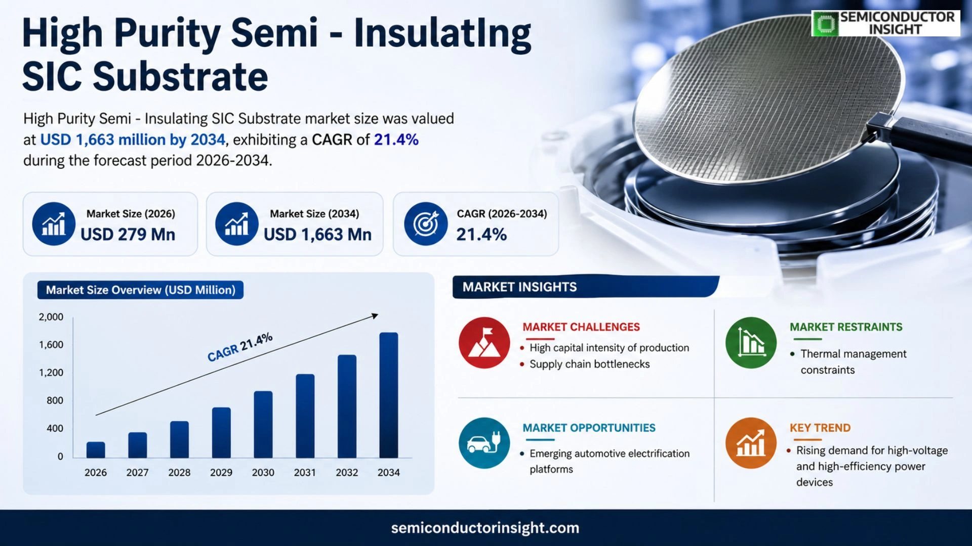
Global High Purity Semi – InsulatIng SIC Substrate market is projected to grow from USD 291 million in 2025 to USD 1,663 million by 2034, exhibiting a CAGR of 21.4% during the forecast period.
A high purity semi‑insulating SiC substrate is a single‑crystal silicon carbide wafer sliced from a SiC boule and engineered for exceptionally low bulk conductivity and RF loss.Semi‑insulating behavior suppresses parasitic leakage, making these wafers essential for high‑power, high‑frequency GaN‑based RF and microwave devices.The upstream value chain comprises ultra‑high‑purity source gases, sublimation/PVT crystal growth with tight control of nitrogen donors or vanadium compensation, followed by precision wafering and double‑side polishing.Downstream, the substrates serve as carriers for GaN/AlGaN epitaxy enabling HEMTs, power amplifiers and MMICs across wireless infrastructure, aerospace and defense applications where thermal management and electrical isolation are critical.
MARKET DRIVERS
Increasing Demand for SiC‑Based Power Devices
High Purity Semi – InsulatIng SIC Substrate Market benefits from the surge in electric‑vehicle platforms that require converters operating at higher voltages and frequencies. Silicon carbide’s superior breakdown field reduces system size, prompting OEMs to procure larger volumes of premium substrates to meet efficiency targets.
Advancements in Crystal Growth Techniques
Recent refinements in the Physical Vapor Transport (PVT) process have driven defect densities below 5 × 10^4 cm⁻², a level previously unattainable at commercial scale. This technical breakthrough translates into lower wafer rejection rates, allowing manufacturers to price high‑purity material more competitively.
➤ Substrates with impurity concentrations under 10^14 cm⁻³ enable switching speeds exceeding 1 GHz while maintaining thermal stability.
As telecom infrastructure upgrades to 5G and beyond, network operators are specifying SiC devices that can tolerate harsher electromagnetic environments. The resulting orders for ultra‑pure SIC wafers reinforce the upward trajectory of the market.
MARKET CHALLENGES
High Capital Intensity of Production
Establishing a line capable of delivering High Purity Semi – InsulatIng SIC Substrate Market volumes requires multi‑million‑dollar investments in crystal growers, metrology equipment, and clean‑room facilities. Smaller players often lack the balance sheet depth to fund such expansions, limiting market entry.
Other Challenges
Supply Chain Bottlenecks
The scarcity of high‑grade silicon sources and the limited number of certified crucible manufacturers create lead times that can exceed six months, pressuring OEM schedules.
MARKET RESTRAINTS
Thermal Management Constraints
Despite SiC’s intrinsic thermal conductivity advantage, integrating ultra‑pure substrates into densely packed modules raises heat‑spread challenges. Designers must allocate additional area for heat sinks, which can erode the size advantages that originally drove adoption of high‑purity SIC wafers.
MARKET OPPORTUNITIES
Emerging Automotive Electrification Platforms
Next‑generation EV architectures that combine on‑board chargers with bidirectional V2G capabilities are specifying SiC devices capable of handling 800 V and higher. This specification gap creates a niche for High Purity Semi – InsulatIng SIC Substrate Market suppliers that can guarantee low leakage currents and high breakdown voltages, opening avenues for premium pricing and long‑term contracts.
High Purity Semi – InsulatIng SIC Substrate Market Trends
Surging Demand from RF Power‑Amplifier Applications
The most visible shift in High Purity Semi – InsulatIng SIC Substrate Market originates from the RF front‑end segment, where GaN‑on‑SiC devices are displacing older silicon technologies. 2024 sales of over 311 K pieces reflect a clear willingness among wireless‑infrastructure and aerospace OEMs to pay a premium for the lower substrate loss and superior thermal conductivity offered by semi‑insulating SiC wafers. As antenna arrays become denser and radar systems push toward higher frequencies, designers require substrates that guarantee electrical uniformity across the whole wafer. This technical necessity translates into larger order volumes for 4‑inch and 6‑inch format wafers, while also prompting early‑stage qualification programmes that lock customers into multi‑year supply contracts.
Other Trends
Supply‑Chain Consolidation and Quality‑Plus‑Cost Competition
Manufacturers are converging around a limited set of high‑purity source materials and sublimation growth reactors, which reduces overall capacity but raises entry barriers for new entrants. Profit margins ranging from 10 % to 30 % illustrate that firms that can consistently deliver low‑defect, uniformly compensated wafers command a pricing advantage. Recent announcements from legacy players to expand to 8‑inch formats underscore a strategic move toward economies of scale, yet the prevailing market narrative emphasizes defect‑control and stable yield over sheer volume. Customers therefore favour suppliers that combine incremental cost reductions with demonstrable quality improvements, a dynamic reshaping of the competitive landscape.
Risk Landscape and Outlook for Material Innovation
While demand from high‑power RF modules remains robust, the market is not immune to cyclical pull‑back linked to telecom‑capex cycles. A temporary inventory correction can appear when network roll‑outs pause, pressuring short‑term order books. Simultaneously, alternative substrate options such as bulk silicon or emerging gallium‑oxide platforms present a price‑sensitive threat in lower‑power segments. Nevertheless, the imperative for higher breakdown strength and thermal dissipation in next‑generation power amplifiers sustains a premium niche for High Purity Semi – InsulatIng SIC Substrate Market participants that continue to push material quality and larger wafer formats. Companies that align process stability with scalable manufacturing are best positioned to capture long‑term programmes across wireless, defense, and industrial sectors.
COMPETITIVE LANDSCAPE
Key Industry Players
High Purity Semi‑Insulating SiC Substrate Competitive Landscape
Wolfspeed remains the benchmark supplier, leveraging its vertically integrated chain from crystal growth to wafer polishing. The company’s focus on large‑format 6‑inch and emerging 8‑inch substrates has allowed it to secure long‑term contracts with major GaN‑on‑SiC device fabs, translating into a stable revenue base that outpaces most rivals. Its ability to maintain impurity concentrations below 10 ppb while delivering wafer‑level uniformity feeds directly into the stringent qualification processes of aerospace and defense customers, reinforcing a defensible market position. Wolfspeed’s recent investment in vanadium‑compensated growth chambers reflects a strategic shift toward improving yield consistency, a factor that directly influences its gross margin ceiling of 30 % in the high‑volume segment.
Beyond the market leader, a constellation of specialized firms occupies the niche corridors of the supply chain. Coherent, with its heritage in optical components, supplies bespoke SiC boules for low‑volume, high‑precision applications, while SiCrystal and STMicroelectronics operate mid‑scale facilities that cater to regional device makers in Europe and Asia. TankeBlue and SICC have differentiated themselves through aggressive cost‑control in bulk crystal growth, targeting mass‑market RF modules where price sensitivity outweighs wafer size. Hebei Synlight Semiconductor and IVSemitec anchor China’s domestic supply, emphasizing rapid capacity expansion to meet the surge in wireless infrastructure projects. Sanan Semiconductor, Hypersics, and KY Semiconductor round out the list, each offering unique value propositions—ranging from proprietary surface‑polish chemistries to deep‑level compensation techniques—that allow them to capture specific customer segments despite the overall concentration of the market.
List of Key High Purity Semi‑Insulating SiC Substrate Companies Profiled
- Wolfspeed
- Coherent
- SiCrystal
- STMicroelectronics
- TankeBlue
- SICC
- Hebei Synlight Semiconductor
- IVSemitec
- Sanan Semiconductor
- Hypersics
- KY Semiconductor
- ROHM Semiconductor
- NTT Advanced Materials
Segment Analysis:
| Segment Category | Sub-Segments | Key Insights |
| By Type |
|
Larger Wafer Formats
|
| By Application |
|
Wireless Infrastructure
|
| By End User |
|
Telecom Equipment Manufacturers
|
| By Growth Driver |
|
Performance Demands
|
| By Market Challenge |
|
High Entry Barriers
|
Regional Analysis: High Purity Semi – Insulating SIC Substrate Market
Asia‑Pacific
Regional suppliers have diversified raw‑material sources, mitigating the impact of geopolitical tensions. Close collaboration between crystal growers and downstream mask makers shortens lead times, enabling manufacturers to keep production schedules tight despite external shocks.
Major fabs allocate a sizable portion of capex to substrate‑optimization programmes, focusing on reducing dislocation density and enhancing doping uniformity. Joint ventures with university labs foster breakthrough crystal‑growth techniques that raise overall material quality.
Targeted subsidies for high‑efficiency power devices lower the effective cost of SiC substrate adoption. Export‑control frameworks remain liberal, allowing regional players to capture market share in emerging economies without excessive licensing hurdles.
OEMs in electric‑vehicle and renewable‑energy applications cite the reliability gains of SiC substrates as a decisive factor, prompting early‑stage contracts that lock in long‑term supply agreements with leading producers.
North America
North America maintains a robust ecosystem of equipment manufacturers and design houses that require high‑purity SiC substrates for high‑frequency power converters. Although domestic production lags behind Asia‑Pacific, strategic investments in advanced epitaxy lines are reshaping the supply picture. Federal research grants emphasize energy‑efficiency standards, nudging automakers toward SiC solutions and creating a credible demand pipeline. The region’s emphasis on intellectual‑property protection also encourages start‑ups to commercialize niche substrate variants, adding depth to the market’s product portfolio.
Europe
European nations combine stringent emissions legislation with a long‑standing commitment to automotive innovation, fostering a favorable climate for SiC substrate uptake. Automotive clusters in Germany and France are integrating SiC‑based modules into next‑generation drivetrains, prompting local fabs to scale up specialty production. Moreover, the EU’s “Green Deal” funding streams support pilot projects that showcase the efficiency benefits of SiC, accelerating customer confidence. Supply‑chain collaborations across the continent reduce reliance on distant sources, though capacity constraints still require occasional imports.
South America
South America’s semiconductor foothold remains modest, yet emerging renewable‑energy installations generate a nascent requirement for high‑efficiency power devices. Countries such as Brazil and Chile are experimenting with SiC‑based inverters to improve grid stability, prompting early exploratory purchases. Local investors are beginning to assess joint‑venture opportunities with Asian manufacturers, aiming to build limited‑run substrate facilities that serve regional power‑conversion projects. The market’s trajectory will hinge on the pace of policy incentives for clean‑energy infrastructure.
Middle East & Africa
In the Middle East & Africa, solar‑farm developers recognize the thermal advantages of SiC substrates for inverter systems operating under high ambient temperatures. While most substrate supply continues to be imported, regional partnerships are forming to establish assembly hubs that add value locally. Government‑led initiatives to diversify energy mixes away from hydrocarbons include pilot programmes that evaluate SiC‑enabled power electronics, offering a potential catalyst for broader adoption as the technology matures.
Report Scope
This market research report provides a comprehensive analysis of the High Purity Semi – InsulatIng SIC Substrate Market , covering the forecast period 2026–2034. It offers detailed insights into market dynamics, technological advancements, competitive landscape, and key trends shaping the industry.
Key focus areas of the report include:
- Market Overview: The report begins with an overview outlining its current market scenario, key growth indicators, and industry transformation drivers. It discusses macroeconomic factors, demand–supply balance, regulatory landscape, and the strategic role of semiconductors in powering advancements across industries such as automotive, telecommunications, consumer electronics, and industrial automation.
- Market Size & Forecast: Historical data and future projections for revenue, unit shipments, and market value across major regions and segments.
- Segmentation Analysis: Detailed breakdown by product type, technology, application, and end-user industry to identify high-growth segments and investment opportunities.
- Regional Insights: Insights into market performance across North America, Europe, Asia-Pacific, Latin America, and the Middle East & Africa, including country-level analysis where relevant.
- Competitive Landscape: Profiles of leading market participants, including their product offerings, R&D focus, manufacturing capacity, pricing strategies, and recent developments such as mergers, acquisitions, and partnerships.
- Technology Trends & Innovation: Assessment of emerging technologies, integration of AI/IoT, semiconductor design trends, fabrication techniques, and evolving industry standards.
- Market Drivers & Restraints: Evaluation of factors driving market growth along with challenges, supply chain constraints, regulatory issues, and market-entry barriers.
- Stakeholder Insights: Insights for component suppliers, OEMs, system integrators, investors, and policymakers regarding the evolving ecosystem and strategic opportunities.
Primary and secondary research methods are employed, including interviews with industry experts, data from verified sources, and real-time market intelligence to ensure the accuracy and reliability of the insights presented.
FREQUENTLY ASKED QUESTIONS:
What is the current market size of High Purity Semi – InsulatIng SIC Substrate Market?
-> High Purity Semi – InsulatIng SIC Substrate market is projected to grow from USD 291 million in 2025 to USD 1,663 million by 2034.
Which key companies operate in High Purity Semi – InsulatIng SIC Substrate Market?
-> Key players include Wolfspeed, Coherent, SiCrystal, STMicroelectronics, TankeBlue, SICC, Hebei Synlight Semiconductor, IVSemitec, Sanan Semiconductor, Hypersics, KY Semiconductor, among others.
What are the key growth drivers?
-> Key growth drivers include rising RF front‑end performance requirements, increasing demand for GaN‑on‑SiC platforms, expanding wireless infrastructure, heightened aerospace and defense electronics needs, and the push for superior thermal management and breakdown strength in high‑power devices.
Which region dominates the market?
-> Asia-Pacific is a dominant region, driven by major semiconductor manufacturing hubs, strong adoption of wireless infrastructure projects, and significant aerospace & defense procurement activities.
What are the emerging trends?
-> Emerging trends include the shift toward “quality‑plus‑cost” strategies, industrialization of larger wafer formats (e.g., 8‑inch), advanced defect‑control techniques during crystal growth and wafer polishing, and increased focus on thermal conductivity and breakdown strength enhancements for next‑generation RF and microwave applications.

Get Sample Report PDF for Exclusive Insights
Report Sample Includes
- Table of Contents
- List of Tables & Figures
- Charts, Research Methodology, and more...
 Download Sample Report PDF