Float Zone Wafer Market Insights
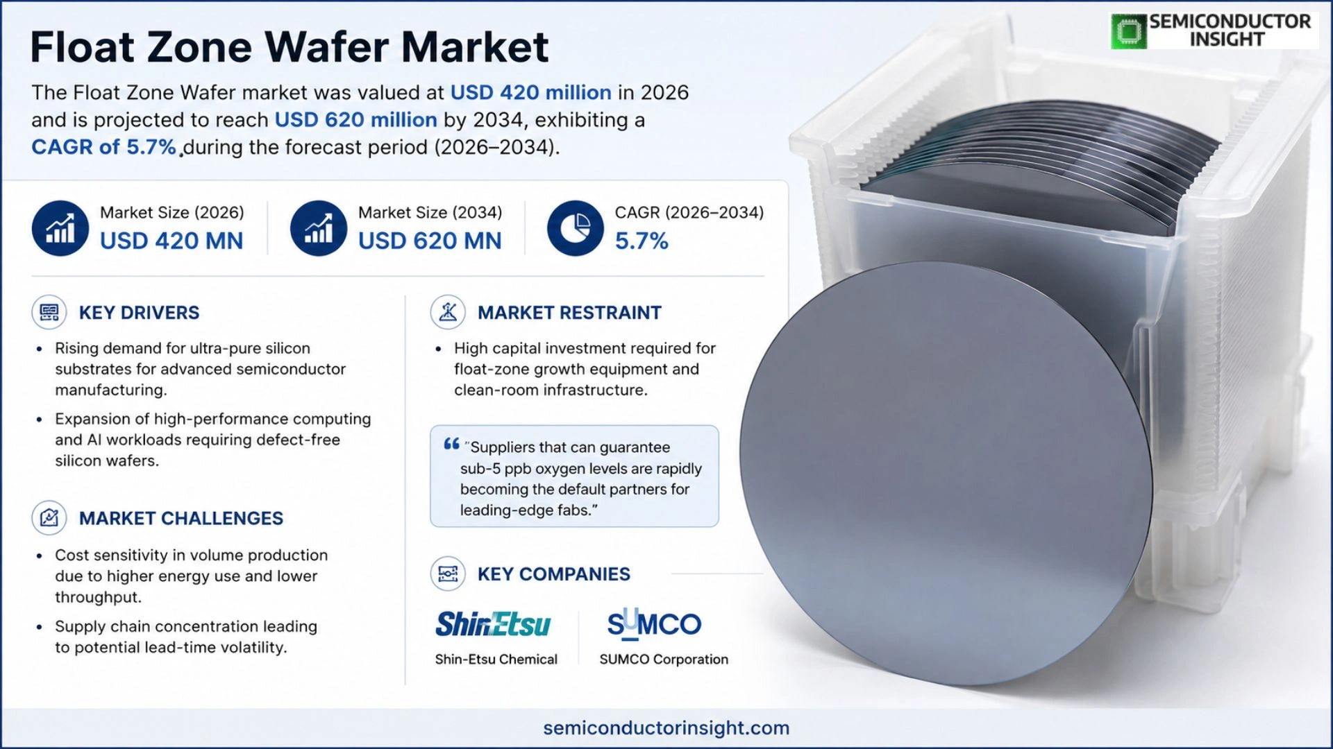
Global Float Zone Wafer market was valued at USD 420 million in 2026 and is projected to reach USD 620 million by 2034, exhibiting a CAGR of 5.7% during the forecast period.
Float Zone Wafer refers to a high‑purity silicon wafer produced by the float‑zone crystal growth technique, which yields superior resistivity uniformity and minimal oxygen contamination compared with conventional Czochralski wafers. These characteristics make it especially suitable for power devices, RF circuits, solar cell substrates and other high‑performance semiconductor applications where low defect density is critical.
The market momentum stems from accelerating adoption of electric vehicles, expanding renewable‑energy installations and increasing demand for efficient power‑electronics modules. While manufacturers benefit from premium pricing linked to performance advantages, they also face pressure from higher production costs and competition from emerging silicon‑on‑insulator solutions. Recent industry activity includes capacity expansions announced by leading suppliers such as Shin‑Etsu Chemical, SUMCO Corporation and Siltronic AG.
MARKET DRIVERS
Rising Demand for Ultra‑Pure Silicon Substrates
Float Zone Wafer Market is being propelled by semiconductor manufacturers’ need for substrates that exhibit minimal impurity levels. As device geometries shrink, even trace contaminants can affect yield, prompting fabs to favor float‑zone material over conventional Czochralski wafers. This shift underscores the strategic importance of purity as a competitive differentiator for chip makers.
Expansion of High‑Performance Computing and AI Workloads
High‑performance computing platforms, especially those supporting AI inference and training, rely on silicon devices that can operate at higher frequencies with lower power loss. Float‑zone wafers deliver the defect‑free crystal structure required for such performance envelopes, making them a preferred input for next‑generation processors. Clients that secure reliable supply lines stand to capture premium margins.
➤ “Suppliers that can guarantee sub‑5 ppb oxygen levels are rapidly becoming the default partners for leading-edge fabs.”
Beyond purity, the manufacturing ecosystem is witnessing tighter integration between wafer suppliers and device designers. Collaborative development cycles enable faster qualification of new process nodes, reducing time‑to‑market for advanced chips. Companies that invest in joint R&D initiatives are positioning themselves to benefit from this collaborative momentum.
MARKET CHALLENGES
Cost Sensitivity in Volume Production
Although float‑zone wafers offer superior electrical characteristics, their production incurs higher energy consumption and lower throughput compared with traditional methods. For manufacturers operating at high volumes, the incremental cost can compress margins, especially when end‑customers exert pricing pressure on commodity components.
Other Challenges
Supply Chain Concentration
A limited number of facilities possess the equipment and expertise to produce float‑zone ingots at scale. Any disruption,whether from equipment failure, raw‑material shortage, or geopolitical tension,can cascade through the supply chain, creating lead‑time volatility for downstream fabs.
MARKET RESTRAINTS
Capital Intensity of Production Facilities
The establishment of a float‑zone crystal growth line requires substantial upfront investment in high‑precision induction heating systems and clean‑room infrastructure. Smaller producers often lack the financial bandwidth to enter the market, reinforcing a barrier that restricts the diversity of supply sources.
MARKET OPPORTUNITIES
Emerging Applications in Power Electronics
Power devices such as silicon‑carbide (SiC) and gallium‑nitride (GaN) transistors increasingly incorporate float‑zone silicon as a substrate to improve thermal conductivity and breakdown voltage. As automotive electrification accelerates, the demand for these high‑efficiency power solutions creates a clear avenue for float‑zone wafer providers to expand their addressable market.
Float Zone Wafer Market Trends
Emerging Shift Toward Smaller Diameters
Float Zone Wafer Market is witnessing a pronounced migration from larger 12‑inch substrates to 2‑inch and 3‑inch formats. 2022 data indicate that 4‑inch wafers still dominate volume, yet the 2‑inch segment grew double‑digit year‑over‑year, driven by demand from sensor and RF circuit makers that favour thinner wafers for tighter integration. This re‑allocation of capacity reduces material waste and aligns with fab lines that are increasingly optimized for high‑mix, low‑volume production. Suppliers such as WaferPro and Shin‑Etsu Chemical have announced line upgrades that prioritize sub‑5‑inch growth, signalling that the industry perceives smaller diameters as a lever for cost control and faster time‑to‑market. For customers, the trend translates into more flexible procurement options and the ability to prototype niche devices without the overhead of 8‑inch or 12‑inch tooling.
Other Trends
Regional Performance Divergence
Across the globe, Float Zone Wafer Market displays a split trajectory. The Americas posted a 17 % increase in sales, buoyed by strong demand for power devices in automotive electrification projects. Europe followed with a 12.6 % rise, anchored by expansion of RF modules for 5G infrastructure. In contrast, the Asia‑Pacific region,traditionally the largest consumer,registered a 2 % contraction, reflecting weaker consumer electronics spend and lingering supply‑chain strain. Japan remained an outlier within the region, posting a 10 % uplift thanks to its focus on solar‑chip applications. The divergence suggests that manufacturers must tailor inventory and pricing strategies to each geography, privileging aggressive growth in the Americas while adopting a more defensive posture in APAC until end‑user demand stabilises.
Application‑Specific Demand Patterns
Application mix is reshaping Float Zone Wafer Market, with solar‑chip and power‑device volumes outpacing traditional logic wafers. Solar‑chip orders grew in tandem with renewable‑energy incentives, pushing the 8‑inch segment to its highest share since 2019. Power‑device manufacturers, capitalising on the shift toward higher voltage architectures, have increased their share of 4‑inch wafers, which offer a balanced compromise between thermal performance and cost. Conversely, logic and memory fabs are moderating consumption of the largest 12‑inch wafers as they transition to advanced node processes that rely more heavily on other wafer technologies. The net effect is a more fragmented demand landscape, prompting suppliers to diversify product portfolios and to invest in flexible manufacturing cells that can switch between size classes with minimal downtime.
COMPETITIVE LANDSCAPE
Key Industry Players
Float Zone Wafer Competitive Overview – 2024
Shin‑Etsu Chemical remains the de‑facto market leader in the float‑zone wafer segment, leveraging its vertically integrated silicon purification network to secure a reliable supply of ultra‑high‑purity billets. The company’s emphasis on 3‑inch and 4‑inch wafers for power‑device applications has entrenched its position with major foundries in Japan, South Korea, and Taiwan. Its ability to couple process optimization with aggressive cost control translates into higher yield margins, compelling OEMs to lock‑in long‑term contracts. Consequently, the market exhibits a concentration‑heavy structure where top‑three firms capture over 55 % of global shipments, reinforcing barriers to entry for new entrants lacking comparable crystal‑growth infrastructure.
Beyond the dominant trio, a cohort of niche specialists expands the competitive field. SUMCO Corporation and Siltronic AG focus on mid‑size 8‑inch wafers, targeting RF and solar‑chip segments where defect density thresholds are critical. GlobalWafers and WaferPro capitalize on flexible production schedules, serving emerging power‑device manufacturers in China and India. Smaller players such as Topsil, Okmetic, and Advanced Semiconductor Materials (ASM) differentiate through proprietary gettering techniques that enable the 12‑inch wafer format for high‑voltage applications. The presence of these diverse capabilities generates a multi‑tiered ecosystem in which technology breadth and regional proximity become decisive factors for channel partners.
List of Key Float Zone Wafer Companies Profiled
- Shin‑Etsu Chemical Co., Ltd.
- Shin‑Etsu Chemical
- SUMCO Corporation
- SUMCO
- Siltronic AG
- Siltronic
- GlobalWafers Co., Ltd.
- GlobalWafers
- WaferPro Inc.
- Topsil Semiconductor Materials AG
- Okmetic Oyj
- Advanced Semiconductor Materials (ASM)
- SK Siltron Co., Ltd.
- MEMC Electronic Materials
Segment Analysis:
| Segment Category | Sub-Segments | Key Insights |
| By Type |
|
4 Inch segment enjoys strong preference among manufacturers because:
|
| By Application |
|
Power Devices dominate due to:
|
| By End User |
|
Analog segment remains pivotal because:
|
| By Wafer Size |
|
Medium (6‑8 inch) emerges as the most versatile because:
|
| By Device Category |
|
High‑Power Devices are driven by:
|
Regional Analysis: Float Zone Wafer Market
North America
Leading fabs have modestly widened their float‑zone float‑up lines, focusing on incremental throughput gains rather than megaprojects, which aligns with the market’s emphasis on quality over volume.
The shift toward wider bandgap devices is prompting manufacturers to explore novel crucible designs that improve thermal gradient control, a subtle but consequential innovation.
Companies are diversifying raw‑silicon sources and building strategic inventories, a response to recent logistical disruptions that highlighted the fragility of single‑supplier models.
Energy‑intensive crystal growth is being examined through the lens of carbon‑footprint reduction, with several plants piloting waste‑heat recovery systems.
Europe
European producers are capitalising on the region’s strong emphasis on automotive electrification, where high‑efficiency power modules benefit from the low defect density of float‑zone wafers. Policy frameworks that reward low‑emission vehicle adoption indirectly lift demand for silicon substrates suited to high‑voltage applications. In parallel, a cluster of research institutes in Germany and the Netherlands is refining dopant control techniques, offering a modest competitive edge to local fabs. While labour costs remain higher than in Asia, the reputational advantage of “Made‑in‑Europe” quality continues to justify premium pricing for niche applications.
Asia‑Pacific
The Asia‑Pacific landscape is defined by rapid scaling of consumer electronics manufacturing, yet the float‑zone segment remains a specialty niche dominated by a few high‑tech players. Companies in Japan and South Korea have invested in process automation to harmonise wafer uniformity across larger diameters, a move that subtly improves yield without inflating cost structures. Meanwhile, emerging markets in Southeast Asia are exploring partnerships with established suppliers to gain footholds in power‑device supply chains, signalling a gradual diffusion of expertise beyond the traditional hubs.
South America
In South America, Float Zone Wafer Market is still nascent, with interest largely stemming from academic projects focused on renewable‑energy converters. Brazil’s recent incentives for semiconductor research have attracted multinational equipment vendors, creating a modest ecosystem of service providers. Although volume remains limited, the region’s abundant hydroelectric power offers a low‑cost energy base that could become attractive for energy‑intensive crystal growth if demand accelerates.
Middle East & Africa
The Middle East & Africa region is witnessing early‑stage engagement with float‑zone technology, primarily through government‑backed pilot facilities aimed at diversifying economies away from hydrocarbons. Partnerships with European research centres are fostering knowledge transfer, especially in contamination‑control protocols. While commercial scale is still years away, the strategic focus on high‑value technology manufacturing positions the region as a potential future supplier of specialised wafers.
Report Scope
This market research report provides a comprehensive analysis of the Float Zone Wafer Market , covering the forecast period 2026–2034. It offers detailed insights into market dynamics, technological advancements, competitive landscape, and key trends shaping the industry.
Key focus areas of the report include:
- Market Overview: The report begins with an overview outlining its current market scenario, key growth indicators, and industry transformation drivers. It discusses macroeconomic factors, demand–supply balance, regulatory landscape, and the strategic role of semiconductors in powering advancements across industries such as automotive, telecommunications, consumer electronics, and industrial automation.
- Market Size & Forecast: Historical data and future projections for revenue, unit shipments, and market value across major regions and segments.
- Segmentation Analysis: Detailed breakdown by product type, technology, application, and end-user industry to identify high-growth segments and investment opportunities.
- Regional Insights: Insights into market performance across North America, Europe, Asia-Pacific, Latin America, and the Middle East & Africa, including country-level analysis where relevant.
- Competitive Landscape: Profiles of leading market participants, including their product offerings, R&D focus, manufacturing capacity, pricing strategies, and recent developments such as mergers, acquisitions, and partnerships.
- Technology Trends & Innovation: Assessment of emerging technologies, integration of AI/IoT, semiconductor design trends, fabrication techniques, and evolving industry standards.
- Market Drivers & Restraints: Evaluation of factors driving market growth along with challenges, supply chain constraints, regulatory issues, and market-entry barriers.
- Stakeholder Insights: Insights for component suppliers, OEMs, system integrators, investors, and policymakers regarding the evolving ecosystem and strategic opportunities.
Primary and secondary research methods are employed, including interviews with industry experts, data from verified sources, and real-time market intelligence to ensure the accuracy and reliability of the insights presented.
FREQUENTLY ASKED QUESTIONS:
What is the current market size of Float Zone Wafer Market?
-> Float Zone Wafer market was valued at USD 420 million in 2026 and is projected to reach USD 620 million by 2034, exhibiting a CAGR of 5.7%
Which key companies operate in Float Zone Wafer Market?
-> Key players include WaferPro, Shin-Etsu Chemical, SUMCO CORPORATION, Siltronic, GlobalWafers, among others.
What are the key growth drivers?
-> Key growth drivers include advancements in semiconductor manufacturing, demand for high‑purity wafers in power devices, and increasing adoption of 5G and electric vehicles.
Which region dominates the market?
-> Asia-Pacific remains the largest region by revenue, while North America shows strong growth rates.
What are the emerging trends?
-> Emerging trends include development of larger diameter (12‑inch) Float Zone wafers, integration with AI‑driven fab processes, and sustainable manufacturing practices.

Get Sample Report PDF for Exclusive Insights
Report Sample Includes
- Table of Contents
- List of Tables & Figures
- Charts, Research Methodology, and more...
 Download Sample Report PDF