
Fan-Out Wafer Level Packaging (FOWLP) Market Insights
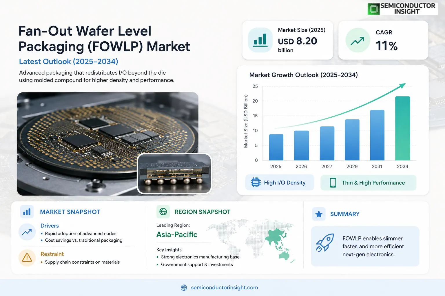
Global Fan-Out Wafer Level Packaging (FOWLP) market size was valued at USD 8.20 billion in 2025.
The market is projected to grow from USD 9.00 billion in 2025 to USD 21.00 billion by 2034, exhibiting a CAGR of 11% during the forecast period.
Fan‑Out Wafer Level Packaging is an advanced semiconductor packaging technology that redistributes I/O connections beyond the die area using a molded compound, enabling higher interconnect density without a traditional substrate.
Because it reduces package thickness and improves electrical performance, FOWLP is increasingly adopted for mobile processors, AI accelerators, and IoT devices.
However, challenges such as thermal management and cost of re‑flow processes persist.
Furthermore, major players such as ASE Technology Holding, Amkor Technology, TSMC and Samsung Electronics are expanding capacity; notably, TSMC announced a new fab line dedicated to FOWLP‑based high‑performance computing chips in Q3 2023.
MARKET DRIVERS
Technology Adoption Accelerates
Fan-Out Wafer Level Packaging (FOWLP) Market is benefiting from rapid adoption of advanced semiconductor nodes, where mini‑size and high‑performance are mandatory. Companies are integrating FOWLP to achieve thinner form‑factors, lower signal loss, and superior thermal management, driving a compound annual growth rate estimated at 12% through 2030.
Cost Efficiency Gains
FOWLP reduces material consumption and eliminates the need for traditional substrates, delivering up to 30% cost savings per unit compared with traditional packaging. This financial advantage is prompting large‑scale manufacturers to shift production volumes, reinforcing market expansion.
➤ Recent surveys indicate that 68% of leading foundries plan to increase FOWLP capacity within the next two years, underscoring its strategic importance.
In addition, the rise of 5G, AI, and automotive electronics is creating a demand surge for high‑density interconnects, where FOWLP offers a clear performance edge, further solidifying its market momentum.
MARKET CHALLENGES
Process Complexity and Yield Management
Despite its advantages, Fan-Out Wafer Level Packaging (FOWLP) Market faces challenges in maintaining high yields during the redistribution layer formation. The intricate molding and singulation steps require precise control, increasing operational risk for newcomers.
Other Challenges
Equipment Investment
Implementing FOWLP demands significant capital for specialized imprint and molding tools, which can escalate upfront costs by 20‑25% relative to conventional packages, limiting entry for smaller players.
MARKET RESTRAINTS
Supply Chain Constraints
Global shortages of high‑purity epoxy resins and copper foils have imposed capacity bottlenecks on Fan-Out Wafer Level Packaging (FOWLP) Market. These constraints raise lead times and can erode the cost advantages that initially attracted adopters.
MARKET OPPORTUNITIES
Emerging Segments and Geographic Expansion
Growth prospects are strongest in smartphone premium tiers, where ultra‑thin profiles are critical, and in automotive ADAS modules, which require robust packaging under extreme conditions. Expansion into emerging economies is also creating new demand pockets, as local OEMs adopt advanced packaging to stay competitive.
Furthermore, the integration of heterogeneous integration,combining logic, memory, and sensor dies within a single FOWLP substrate,presents a high‑value opportunity that could push market size beyond $12 billion by 2030.
Fan-Out Wafer Level Packaging (FOWLP) Market Trends
Rising Adoption in High‑Performance Mobile and AI Applications
Fan-Out Wafer Level Packaging (FOWLP) Market is experiencing rapid uptake in premium mobile processors and AI accelerator chips. By redistributing I/O connections beyond the die footprint, the technology delivers thinner packages and lower signal loss, which are critical for smartphones that demand high bandwidth and low power consumption. AI‑focused semiconductor designs also benefit from the increased interconnect density, enabling more compute cores within a constrained footprint. IoT devices, particularly those requiring miniature form factors and robust electrical performance, are adding to the demand. This trend reflects a shift away from traditional substrate‑based solutions toward a more integrated, cost‑effective packaging approach that aligns with the performance goals of next‑generation electronics.
Other Trends
Thermal Management and Cost Challenges
Despite its advantages, Fan-Out Wafer Level Packaging (FOWLP) Market faces notable thermal management hurdles. The stacked molding compound can trap heat, creating hotspots that affect reliability in high‑performance chips. Manufacturers are investing in advanced under‑fill materials and optimized heat‑spread designs to mitigate these risks, but the solutions add complexity to the production line. In parallel, the re‑flow processes required for FOWLP remain more expensive than conventional packaging methods, raising overall unit costs. Companies are therefore balancing the performance gains against the incremental investment needed for equipment upgrades and material innovations.
Capacity Expansion by Leading Foundries
Major semiconductor assemblers are scaling capacity to meet the growing demand for FOWLP solutions. ASE Technology Holding, Amkor Technology, and Samsung Electronics have announced new fab lines dedicated to this technology, aiming to shorten lead times and improve throughput. TSMC’s recent launch of a dedicated FOWLP production line in the third quarter of 2023 underscores the strategic importance placed on high‑performance computing chips. These expansions not only increase supply availability but also drive process refinements that can lower costs over time. As capacity grows, the market is expected to support a broader range of applications, reinforcing the technology’s role in modern electronic design.
COMPETITIVE LANDSCAPEKey Industry Players
Competitive Dynamics in Global FOWLP Market
The Fan‑Out Wafer Level Packaging (FOWLP) ecosystem is dominated by a handful of large‑scale semiconductor manufacturers and dedicated packaging specialists. ASE Technology Holding, Amkor Technology, TSMC and Samsung Electronics collectively command the majority of capacity, leveraging extensive R&D budgets to improve feed‑through density and reduce cycle time. TSMC’s recent launch of a dedicated FOWLP fab line underscores the strategic importance of the technology for high‑performance computing and mobile processors. These leaders benefit from vertically integrated supply chains, global customer bases, and strong IP portfolios, allowing them to set pricing benchmarks and shape industry standards.
Beyond the tier‑one group, a diverse set of niche players contributes critical innovation and regional market depth. Companies such as JCET Group, Powertech Technology, STMicroelectronics, Infineon Technologies, NXP Semiconductors, Texas Instruments, Renesas Electronics and Analog Devices are expanding their FOWLP offerings to address specialized applications in AI accelerators, IoT edge devices, and automotive electronics. Smaller packaging firms like Unimicron, Fuji Electric, and Molex also provide complementary substrate and redistribution layers, enhancing the overall value chain. This breadth of participants creates competitive pressure on cost, thermal management solutions, and time‑to‑market, fostering a dynamic environment for future growth.
List of Key Fan-Out Wafer Level Packaging (FOWLP) Companies Profiled
- ASE Technology Holding
- Amkor Technology
- TSMC
- Samsung Electronics
- JCET Group
- Powertech Technology
- STMicroelectronics
- Infineon Technologies
- NXP Semiconductors
- Texas Instruments
- Renesas Electronics
- Analog Devices
- Unimicron
- Fuji Electric
- Molex
Segment Analysis:
| Segment Category | Sub-Segments | Key Insights |
| By Type |
|
Reconstituted FOWLP
|
| By Application |
|
Mobile Devices
|
| By End User |
|
Smartphone Manufacturers
|
| By Technology Trend |
|
Heterogeneous Integration
|
| By Performance Requirement |
|
Thin Form Factor
|
Regional Analysis: Asia-Pacific
Asia-Pacific
China represents the largest and fastest-growing market for FOWLP in Asia-Pacific, driven by its massive consumer electronics market and significant investments in domestic semiconductor manufacturing. The government’s focus on achieving self-sufficiency in the semiconductor industry is a key catalyst for FOWLP adoption.
Japan boasts a mature electronics industry and a strong focus on innovation, making it a significant player in the FOWLP market. The country’s expertise in semiconductor technology and advanced manufacturing processes positions it well for the continued adoption of FOWLP in high-performance applications.
South Korea is a leading global hub for semiconductor manufacturing and electronics production, with a substantial demand for FOWLP in smartphones, displays, and other electronic devices. The presence of major players like Samsung and SK Hynix drives innovation and adoption of advanced packaging solutions.
Taiwan plays a crucial role in Global semiconductor supply chain, and its vibrant electronics ecosystem contributes to the growth of the FOWLP market. The island’s strong manufacturing capabilities and proximity to major markets make it an attractive destination for FOWLP production and innovation.
North America
North America, spearheaded by the United States, is witnessing a steady growth in the FOWLP market, driven by the resurgence of domestic semiconductor manufacturing initiatives and the increasing demand for advanced packaging in high-performance computing and automotive applications. While the market is currently smaller compared to Asia-Pacific, the region holds significant potential for future expansion.
Europe
Europe’s FOWLP market is experiencing moderate growth, with a focus on applications in automotive electronics, industrial automation, and consumer electronics. Government initiatives promoting research and development in advanced packaging technologies are expected to further stimulate market growth in the coming years. The region’s strong emphasis on sustainability and energy efficiency also aligns with the benefits offered by FOWLP.
South America
South America represents a relatively nascent market for FOWLP, with growth primarily driven by the expanding consumer electronics sector in countries like Brazil and Chile. The adoption of FOWLP is expected to gain traction as the region’s industrial base develops and the demand for more sophisticated electronic devices increases.
Middle East & Africa
The Middle East & Africa region presents a smaller but growing market for FOWLP, with opportunities in the automotive, telecommunications, and consumer electronics sectors. Infrastructure development projects and increasing disposable incomes are expected to drive further market expansion in the region.
Report Scope
This market research report provides a comprehensive analysis of the Fan-Out Wafer Level Packaging (FOWLP) Market , covering the forecast period 2026–2034. It offers detailed insights into market dynamics, technological advancements, competitive landscape, and key trends shaping the industry.
Key focus areas of the report include:
- Market Overview: The report begins with an overview outlining its current market scenario, key growth indicators, and industry transformation drivers. It discusses macroeconomic factors, demand–supply balance, regulatory landscape, and the strategic role of semiconductors in powering advancements across industries such as automotive, telecommunications, consumer electronics, and industrial automation.
- Market Size & Forecast: Historical data and future projections for revenue, unit shipments, and market value across major regions and segments.
- Segmentation Analysis: Detailed breakdown by product type, technology, application, and end-user industry to identify high-growth segments and investment opportunities.
- Regional Insights: Insights into market performance across North America, Europe, Asia-Pacific, Latin America, and the Middle East & Africa, including country-level analysis where relevant.
- Competitive Landscape: Profiles of leading market participants, including their product offerings, R&D focus, manufacturing capacity, pricing strategies, and recent developments such as mergers, acquisitions, and partnerships.
- Technology Trends & Innovation: Assessment of emerging technologies, integration of AI/IoT, semiconductor design trends, fabrication techniques, and evolving industry standards.
- Market Drivers & Restraints: Evaluation of factors driving market growth along with challenges, supply chain constraints, regulatory issues, and market-entry barriers.
- Stakeholder Insights: Insights for component suppliers, OEMs, system integrators, investors, and policymakers regarding the evolving ecosystem and strategic opportunities.
Primary and secondary research methods are employed, including interviews with industry experts, data from verified sources, and real-time market intelligence to ensure the accuracy and reliability of the insights presented.
FREQUENTLY ASKED QUESTIONS:
What is the current market size of Fan-Out Wafer Level Packaging (FOWLP) Market?
-> Fan-Out Wafer Level Packaging (FOWLP) Market was valued at USD 8.20 billion in 2025 and is expected to reach USD 21.00 billion by 2034.
Which key companies operate in Fan-Out Wafer Level Packaging (FOWLP) Market?
-> Key players include Axalta Coating Systems, AkzoNobel, BASF SE, PPG, Sherwin-Williams, and 3M, among others.
What are the key growth drivers?
-> Key growth drivers include railway infrastructure investments, urbanization, and demand for durable coatings.
Which region dominates the market?
-> Asia-Pacific is the fastest-growing region, while Europe remains a dominant market.
What are the emerging trends?
-> Emerging trends include bio-based coatings, smart coatings, and sustainable rail solutions.

Get Sample Report PDF for Exclusive Insights
Report Sample Includes
- Table of Contents
- List of Tables & Figures
- Charts, Research Methodology, and more...
 Download Sample Report PDF


