
Key Statistics
Key Takeaways
- Asia Pacific is the largest regional market because Taiwan, China and South Korea combine leading foundry capacity, design ecosystems, electronics manufacturing and dense supplier networks; the fabless model scales most efficiently where design companies can access advanced process, packaging and manufacturing partners without owning fabs.
- Logic ICs and compute-oriented designs represent the strategic value center as AI accelerators, networking processors, mobile application processors and custom silicon absorb advanced-node capacity and premium packaging. Analog, microcontrollers, sensors and connectivity remain broad-volume categories with different node economics.
- Servers, data centers and AI are the fastest-changing application pool. NVIDIA, AMD and Broadcom are reporting very large AI-related semiconductor demand, while hyperscalers increasingly seek custom accelerators and networking silicon, expanding the addressable opportunity for fabless architecture and IP teams.
- The fabless model converts fixed manufacturing cost into strategic supplier dependence. Companies avoid owning leading-edge fabs but become highly dependent on foundry allocation, advanced packaging, HBM availability, EDA tools, semiconductor IP and geographic supply-chain resilience.
- Advanced-node concentration is the principal structural risk. TSMC remains central to leading-edge production, so capacity, yield, export controls and packaging bottlenecks can influence the revenue trajectory of many nominally independent chip designers at the same time.
- Diversification beyond smartphones is reshaping the competitive landscape. Qualcomm is targeting data centers, automotive and IoT; AMD is expanding in AI and server compute; Broadcom is scaling AI accelerators and networking; and specialized design houses increasingly monetize domain-specific architectures rather than competing only in general-purpose CPUs.
Fabless Semiconductor Market Overview
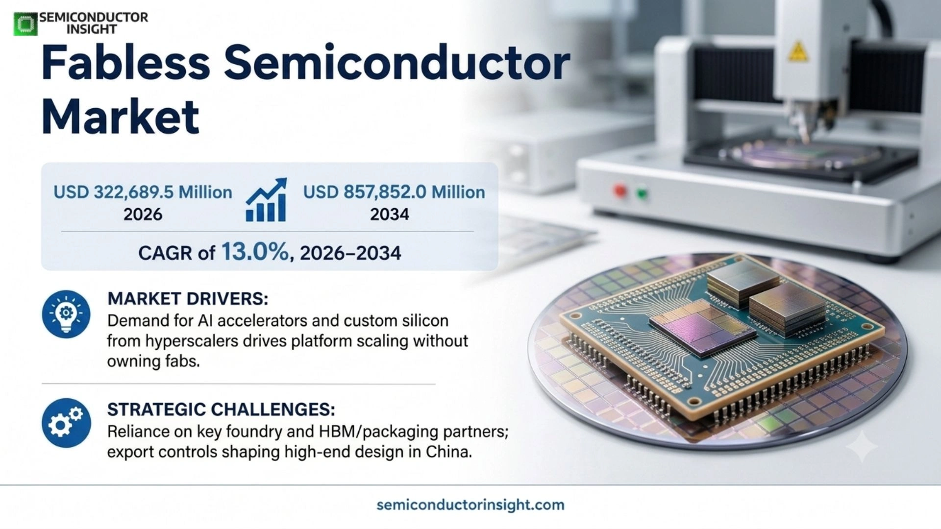
Fabless Semiconductor Market was valued at USD 285,565.9 million in 2025, is estimated at USD 322,689.5 million in 2026, and is projected to reach USD 857,852.0 million by 2034, representing an anchor-derived CAGR of 13.0% during 2026–2034. Asia Pacific is the largest regional market in 2025 on the controlling report scope, while the commercial growth mechanism is increasingly shaped by AI accelerators, custom compute, data-center networking, automotive silicon and continued outsourcing of capital-intensive wafer fabrication to foundry partners.
A fabless semiconductor company designs and commercializes integrated circuits while outsourcing wafer fabrication to external foundries. The model separates the economics of chip architecture, IP, software and customer engagement from the extremely capital-intensive manufacturing assets required at advanced process nodes. This allows successful design companies to scale revenue rapidly without financing leading-edge fabs, but it also means manufacturing capacity, yield and packaging are external dependencies that must be managed strategically.
The controlling report page segments the market across analog ICs, logic ICs, microcontrollers and microprocessors, memory ICs, discrete devices, optoelectronics and sensors, with applications spanning mobile devices, PCs, automotive, industrial and medical, servers/data centers/AI, network infrastructure, appliances and other uses. That breadth is important because the fabless model is not one technology segment; it is an operating model applied across multiple semiconductor categories and process nodes.
AI has increased the economic value concentrated in design. A high-performance accelerator combines architecture, interconnect, memory interfaces, software ecosystems and packaging choices, while production is executed by foundries and OSAT/advanced-packaging partners. The result is a market where a relatively small number of fabless companies can create very large revenue streams if they secure leading-edge capacity and establish platform-level software or customer lock-in.
At the same time, not every fabless company needs the newest process node. Analog, mixed-signal, microcontroller, connectivity and sensor suppliers often optimize mature-node economics, long product life and application-specific performance. This creates two overlapping competitive systems: one dominated by leading-edge compute and packaging constraints, and another where design reuse, channel reach, embedded qualification and cost control matter more than transistor density.
Segment Analysis: By Type
By product type, the source scope includes Analog ICs, Logic IC, Microcontroller and Microprocessor ICs, Memory IC, Discrete, Optoelectronics and Sensors. Logic and compute designs capture a disproportionate share of strategic attention because AI and data-center platforms use advanced nodes and packaging, while analog, MCU, sensor and connectivity portfolios provide diversified volume and longer product cycles.
| Type | Technical role | Market position |
|---|---|---|
| Analog ICs | Power management, signal conditioning, data conversion and interface functions that connect digital processing with real-world voltages and sensors. Many products use mature or specialty nodes where process stability, high-voltage capability and analog performance matter more than minimum geometry. | A broad and durable fabless category with long design-in cycles. Competition is driven by application expertise, product breadth and customer qualification; manufacturing dependence is spread across specialty foundries rather than concentrated only at the newest nodes. |
| Logic IC | Application processors, GPUs, AI accelerators, networking ASICs, FPGAs and other digital logic products whose value is created by architecture, software and high transistor density. | Strategic value leader. AI and data-center demand have pushed advanced logic to the center of fabless revenue growth, but dependence on leading-edge foundry and advanced packaging capacity is also highest in this category. |
| Microcontroller and Microprocessor ICs | Embedded processors and control devices used across automotive, industrial, consumer and IoT systems. Product families combine compute cores, memory, connectivity and peripherals around specific application requirements. | A large design-in market where software tools, ecosystem continuity and qualification matter. Mature and mid-range nodes remain commercially important, while higher-performance automotive and edge-AI processors pull selected designs toward more advanced processes. |
| Memory IC | Fabless participation focuses on controllers, specialty memories and architecture/IP around storage and memory subsystems rather than ownership of commodity DRAM or NAND mega-fabs. | Smaller than vertically integrated commodity memory manufacturing in the fabless model, but strategically relevant where controller design, interface IP and specialized nonvolatile memory create differentiation. |
| Discrete | Power and switching devices designed by asset-light semiconductor companies and manufactured through external foundries or specialized partners. | A selective segment where packaging, process specialization and reliability can matter as much as front-end design. Competition overlaps with integrated device manufacturers, so fabless companies need clear application or cost advantages. |
| Optoelectronics | Optical, photonic and display-related semiconductor designs used in communications, sensing and consumer electronics. | Growth is linked to data-center optics, sensing and high-speed connectivity. Specialized process platforms and packaging often matter more than pure CMOS scaling, creating opportunities for focused design companies. |
| Sensors | Image, motion, environmental and other sensing ICs whose value combines semiconductor design with application-specific signal processing and algorithms. | A diversified category with strong exposure to automotive, mobile, industrial and IoT demand. Design wins can persist for several product generations, but qualification and packaging requirements create meaningful switching costs. |
Why does the fabless model span both leading and mature nodes?
Fabless economics reward choosing the process that maximizes product value rather than automatically selecting the smallest geometry. AI accelerators and high-end mobile processors need dense advanced logic, while analog, microcontrollers, sensors and connectivity chips may achieve better cost, voltage or reliability on mature nodes. This flexibility is a core advantage of outsourcing: design companies can use different foundries and processes by product family, although each additional manufacturing relationship adds qualification and supply-chain complexity.
Segment Analysis: By Application
By application, the source scope covers Mobile devices, PCs, Automotive, Industrial & medical, Servers & Data Center & AI, Network infrastructure, Appliances/Consumer Goods and Others. Mobile remains a major installed demand pool, while servers, data centers and AI are the strongest current growth engine because accelerator, networking and custom-compute spending has expanded rapidly.
| Application | Demand characteristics |
|---|---|
| Mobile devices | Smartphones and tablets use application processors, modems, RF, power management, display, sensor and connectivity ICs. Fabless suppliers win through integration, modem/IP capability, power efficiency and platform relationships. Growth is mature relative to AI, but enormous shipment scale keeps mobile strategically important. |
| PCs | Client CPUs, GPUs, connectivity and peripheral controllers support consumer and commercial PCs. The market is cyclical and increasingly shaped by AI-PC features, but design competition remains anchored in performance per watt, software compatibility and OEM platform wins. |
| Automotive | ADAS, infotainment, connectivity, domain controllers and power-management systems increase semiconductor content per vehicle. Automotive design wins are valuable because qualification is long and production programs persist for years; suppliers must support functional safety, traceability and long product availability. |
| Industrial & medical | Industrial automation, robotics, instrumentation and medical equipment favor reliable embedded processing, analog, sensing and connectivity. Volumes are lower than consumer markets, but product lifecycles are longer and customers value technical support and continuity over rapid annual redesign. |
| Servers & Data Center & AI | Fastest-changing demand pool. AI accelerators, CPUs, DPUs, switches, NICs and custom ASICs use advanced logic, HBM interfaces and premium packaging. High system value supports very large semiconductor spending, but access to foundry and CoWoS-class packaging capacity is a critical commercial dependency. |
| Network infrastructure | Routers, switches, wireless infrastructure and optical transport use high-speed networking silicon, DSPs, RF and connectivity ICs. Demand is tied to cloud and carrier capex, with strong emphasis on bandwidth per watt and standards compliance. |
| Appliances/Consumer Goods | TVs, appliances, wearables and other devices use MCUs, connectivity, display drivers and power-management chips. This market is highly cost-sensitive and often relies on mature nodes, creating opportunities for fabless suppliers with efficient reference designs and broad distribution. |
| Others | Aerospace, defense, specialty computing and emerging IoT applications create smaller but differentiated niches. Customers may prioritize security, long lifecycle, temperature range or specialized interfaces, supporting focused design companies. |
Why is AI changing fabless semiconductor economics?
AI increases the amount of economic value captured by architecture and software while simultaneously raising dependence on manufacturing partners. Leading accelerators require advanced nodes, HBM and complex packaging, so revenue can scale faster than owned assets but only if a design company secures external capacity across several constrained stages. This rewards firms with strong foundry relationships, large purchase commitments and software ecosystems, while smaller companies increasingly use chiplets, licensed IP and specialized foundry services to reduce development risk.
Regional Analysis
Asia Pacific is the largest fabless semiconductor region because Taiwan anchors leading foundry manufacturing, China has a large and expanding design ecosystem, South Korea provides memory and semiconductor infrastructure, and the broader region contains the electronics manufacturing customers that convert designs into devices and systems. North America remains the global center for many highest-value fabless architectures and AI platforms.
How do regional roles differ in the fabless semiconductor value chain?
The fabless model creates a geographic separation between design leadership and manufacturing concentration. North America hosts many of the world’s largest design companies and software ecosystems. Asia Pacific combines large design communities with the foundry, packaging and electronics manufacturing infrastructure that turns designs into volume. Europe is strong in automotive, industrial and communications specialties. South America and Middle East & Africa are smaller direct design markets but create downstream demand and selected design-talent opportunities.
| Region | Position | Growth outlook | Demand profile | What decides supplier selection |
|---|---|---|---|---|
| Asia Pacific | Largest | Highest manufacturing-linked scale | Foundry + packaging + design ecosystem | Advanced-node access, cost, packaging capacity, local customer support |
| North America | Highest-value design hub | Very high | AI, cloud, networking and platform design | Foundry allocation, HBM/packaging access, software ecosystem, export compliance |
| Europe | Specialty design center | Moderate-High | Automotive + industrial + communications | Qualification, long lifecycle, automotive safety and regional supply resilience |
| South America | Emerging demand market | Moderate from small base | Consumer + industrial + cloud demand | Distribution, landed cost and design-support availability |
| Middle East & Africa | Emerging design/investment market | Moderate from small base | Data centers + sovereign technology investment | Talent, IP access, ecosystem depth and trusted supply |
Competitive Landscape
Competition is driven by architecture, software ecosystems, IP, customer platforms and access to external manufacturing. The largest fabless companies can spend billions on R&D and reserve significant foundry and packaging capacity, while smaller firms compete through domain-specific chips, licensed IP and focused customer relationships.
AI has widened the revenue gap between top-tier design platforms and smaller fabless companies. NVIDIA’s accelerator and software ecosystem, AMD’s CPU/GPU portfolio and Broadcom’s custom AI and networking business show how a successful architecture can scale rapidly without owning wafer fabs. The trade-off is dependence on foundry, HBM and advanced packaging partners that must expand in parallel.
Mobile remains a second major competitive system led by companies such as Qualcomm and MediaTek. Here integration of CPU, GPU, modem, RF, AI and power efficiency matters as much as raw compute performance. Mature smartphone growth has encouraged suppliers to reuse their IP in automotive, IoT, PCs and data centers, increasing competition across previously separate semiconductor categories.
Custom silicon is becoming more important because hyperscalers want accelerators and networking devices optimized for their own workloads. Broadcom, Marvell and design-service specialists can monetize deep interface, SerDes and implementation expertise, while foundries provide manufacturing. This model can support very large programs but creates customer concentration risk and requires reliable execution on advanced nodes.
China’s fabless ecosystem adds competitive pressure in mature and selected advanced categories, but export controls shape access to high-end compute technology. This can redirect local design effort toward domestic process availability, specialized accelerators, MCUs, sensors and connectivity, while international companies must build compliance into customer and foundry workflows.
| Competitive tier | Representative companies | Commercial basis |
|---|---|---|
| Global AI and compute leaders | NVIDIA; AMD; Broadcom; Qualcomm; Marvell | Compete through architecture, software, advanced-node access, networking and platform-scale customer relationships. |
| Large Asian diversified fabless suppliers | MediaTek; Novatek; Realtek; HiSilicon; GigaDevice; Silicon Motion; Goodix | Use proximity to electronics manufacturing, broad product portfolios, cost-efficient execution and strong regional customer relationships. |
| Specialty analog, interface and design players | Monolithic Power Systems; Cirrus Logic; Semtech; Synaptics; Allegro MicroSystems; Nordic Semiconductor; GUC; Alchip | Win through application expertise, mixed-signal performance, design services, connectivity, advanced implementation or focused customer programs. |
Companies profiled in the source scope
NVIDIA Corporation, Qualcomm, Broadcom Limited, Advanced Micro Devices (AMD), MediaTek, Marvell Technology Group, Novatek Microelectronics Corp., Tsinghua Unigroup, Realtek Semiconductor Corporation, OmniVision Technology, Inc., Monolithic Power Systems, Inc. (MPS), Cirrus Logic, Inc., Socionext Inc., LX Semicon, HiSilicon Technologies, Synaptics, Allegro MicroSystems, Himax Technologies, Semtech, Global Unichip Corporation (GUC), Hygon Information Technology, GigaDevice, Silicon Motion, Ingenic Semiconductor, Raydium, Goodix Limited, Sitronix, Nordic Semiconductor, Silergy, Shanghai Fudan Microelectronics Group, Alchip Technologies, FocalTech, MegaChips Corporation, Elite Semiconductor Microelectronics Technology, SGMICRO.
Production Capacity Analysis
Fabless companies do not own the front-end factories that define the model, so ‘production capacity’ is best understood as accessible foundry, advanced packaging, memory and backend capacity. The decisive constraint is whether a design company can secure the right process node and packaging technology at the time its product must launch.
Leading-edge wafer capacity is highly concentrated. TSMC’s quarterly mix shows how much revenue is already produced at advanced nodes, and large AI customers reserve capacity well before product launch. Fabless companies therefore use multi-year forecasts, prepayments and close technology collaboration to protect supply, making procurement and foundry engineering strategic functions rather than administrative sourcing tasks.
Advanced packaging has become a co-equal capacity gate for AI chips. A leading-edge die that cannot be integrated with HBM and high-density interconnect on schedule does not create revenue. This has increased the importance of packaging roadmaps, substrate supply and memory allocation in fabless product planning, especially for accelerators and networking devices.
Mature-node capacity remains important for analog, MCUs, sensors and connectivity. Those products benefit from depreciated or specialty process technologies and can remain in production for many years. Fabless suppliers must balance cost against geographic diversification and long-term availability because customers in automotive and industrial markets may require support far beyond consumer product cycles.
| Capacity layer | Where it concentrates | Commercial constraint |
|---|---|---|
| Leading-edge logic foundry | Taiwan-led, with additional U.S., Korea and global capacity | Allocation, yield, node maturity and geopolitical concentration determine whether high-end fabless designs can ramp on schedule. |
| Mature and specialty foundry | Taiwan, China, U.S., Europe, Japan and Southeast Asia-linked ecosystems | Process specialization, cost, long-term availability and analog/RF/high-voltage capability are more important than minimum geometry. |
| Advanced packaging | Taiwan and broader Asian OSAT/foundry ecosystem, with global expansion | HBM integration, 2.5D/3D capacity, interposers and substrates can constrain AI product shipments even when wafers are available. |
| Memory and components | Korea, U.S., Japan, Taiwan and global suppliers | HBM, high-speed memory and critical substrates/interfaces must scale in step with accelerator demand, creating multi-supplier coordination risk. |
Market Dynamics
The market benefits from the economic leverage of concentrating capital in design instead of fabs, but that leverage creates dependence on a concentrated manufacturing ecosystem. AI, automotive and custom silicon are expanding revenue opportunities while foundry capacity, packaging, export controls and development cost determine which design companies can convert architecture into volume shipments.
Market Drivers
| Factor | Directional impact | Why it matters |
|---|---|---|
| AI accelerators and custom compute | High | AI training and inference expand demand for GPUs, accelerators, networking and hyperscaler-specific ASICs, all well suited to the fabless model. |
| Outsourced foundry economics | High | Avoiding leading-edge fab ownership allows design companies to direct capital toward architecture, software and customer platforms while using specialist manufacturers. |
| Automotive semiconductor content | Medium-High | ADAS, connectivity, infotainment and centralized compute increase the number and value of designed ICs per vehicle and reward long-lived design wins. |
| 5G, edge and IoT diversification | Medium | Connectivity and edge processing create opportunities across mobile, industrial and consumer devices using both advanced and mature nodes. |
AI rewards architecture and software more than factory ownership
Generative AI has created extraordinary demand for accelerators and networking devices whose value is defined by architecture, memory hierarchy, interconnect and software. Fabless companies can scale these platforms quickly by outsourcing wafer fabrication, allowing revenue to grow much faster than owned physical assets. The model is especially powerful when software ecosystems create recurring customer preference and high switching costs.
Foundry specialization lowers the barrier to manufacturing world-class chips
A design company can access process technologies developed by specialist foundries without financing an entire leading-edge fab. That makes it possible for multiple architecture companies to compete at advanced nodes and lets smaller firms use mature or specialty processes tailored to their products. The trade-off is that foundry relationships and capacity commitments become central to competitive strategy.
Automotive design wins create durable revenue streams
Vehicle platforms increasingly use centralized compute, ADAS processors, connectivity and power-management ICs. Qualification cycles are long, but once a fabless supplier is designed into a vehicle architecture, production can continue for years and extend across model variants. This supports high customer lifetime value and encourages suppliers to invest in functional safety, software and long-term supply commitments.
Diversification lets established IP move into adjacent markets
Qualcomm’s expansion from handsets into automotive, IoT and data centers illustrates how reusable CPU, modem, AI, connectivity and software IP can address multiple end markets. Similar portfolio expansion reduces dependence on mature smartphone cycles and increases the economic return on large R&D investments, supporting continued fabless market growth.
Market Restraints
| Factor | Directional impact | Why it matters |
|---|---|---|
| Advanced-node foundry concentration | High | Many leading fabless designs depend on a small number of advanced foundry lines, exposing revenue to allocation, yield and geographic disruption. |
| Advanced packaging and HBM bottlenecks | High | AI chips require packaging and memory capacity that must scale with wafers; shortages in any stage can cap finished accelerator shipments. |
| Rising design and tape-out cost | Medium-High | Leading-edge masks, EDA, IP verification and engineering teams make each new advanced-node design extremely expensive, raising the scale required to compete. |
| Export controls and geopolitical fragmentation | Medium-High | Restrictions on advanced computing products and foundry due diligence complicate customer access, product planning and manufacturing relationships. |
Fabless does not mean capacity risk disappears
Outsourcing removes factory ownership from the balance sheet but does not remove the need for manufacturing capacity. When many successful designs target the same leading node or packaging technology, allocation can become the binding constraint. Large customers can secure supply through commitments and close co-development, while smaller companies face schedule risk or less favorable economics.
AI supply depends on an entire constrained stack
An accelerator requires more than a logic die. HBM, substrates, interposers, advanced packaging and networking components must all be available in compatible volumes. A fabless company may have sufficient wafer starts but still miss revenue if packaging or memory supply lags. This makes cross-supply-chain planning a core capability and increases working-capital and forecasting requirements.
Leading-edge design cost raises entry barriers
Mask sets, EDA tools, verification, IP licenses and engineering headcount become more expensive as process complexity increases. A failed tape-out can destroy substantial time and capital. Startups therefore need either exceptional funding, chiplet strategies or focused markets where mature nodes can deliver differentiated value without matching the development budget of the largest companies.
Geopolitical rules can change the addressable market
Advanced-computing export controls and foundry due-diligence requirements can restrict sales or require product modifications for specific customers and geographies. Fabless firms must account for these rules before tape-out because a chip designed around a restricted performance threshold may lose access to a major market. Compliance therefore influences architecture and commercial strategy, not just shipping paperwork.
Market Opportunities
Custom AI silicon for hyperscalers
Cloud companies increasingly want workload-specific accelerators and networking devices that optimize performance, power and total ownership cost. Fabless ASIC specialists and design-service companies can capture large programs by combining architecture, SerDes, packaging and foundry execution. Customer concentration is high, but a successful program can create substantial multi-generation revenue.
Automotive centralized compute
Vehicles are consolidating functions into domain and central processors, increasing compute and connectivity requirements. Fabless suppliers that provide scalable processors, AI acceleration, networking and software can win high-value platforms and extend the same architecture across multiple vehicle classes, creating long qualification-protected revenue streams.
Chiplets and reusable semiconductor IP
Chiplet architectures can reduce the need to place every function on the newest node and allow companies to reuse proven compute, I/O or accelerator blocks. This lowers some development risk and creates opportunities for IP, interface and design-service specialists that can make heterogeneous components work together within advanced packages.
Regional and sovereign design ecosystems
Governments and large customers increasingly want more control over strategic compute and communications technologies. Because building a leading-edge fab is extraordinarily expensive, fabless design is a more accessible entry point for new regional ecosystems. Local design centers can use global foundries while developing domestic IP, engineering talent and application-specific chips.
Supply Chain Analysis
Architecture and IP. The highest-margin value is often created before a wafer is processed. Architecture, algorithms, software, SerDes, modem, memory and accelerator IP determine product differentiation. Large fabless companies internalize core IP while licensing selected blocks, whereas startups use more third-party IP to reduce schedule and verification risk.
EDA and tape-out. Foundry process design kits, EDA tools and verification workflows translate the architecture into manufacturable geometry. Errors are expensive because advanced mask sets and schedule delays carry substantial cost. Close collaboration between design teams, EDA vendors and foundries is therefore critical to first-pass success.
Foundry and packaging. External manufacturers carry the capital burden of wafer fabrication and increasingly advanced packaging. Fabless customers trade asset-light economics for dependence on allocation, yield and supplier roadmaps. For AI products, packaging and HBM have become capacity decisions that must be planned alongside front-end wafers.
Go-to-market and platforms. The strongest fabless companies sell more than silicon. Software stacks, developer tools, reference designs and long-term OEM relationships create switching costs and turn a chip into a platform. This raises gross-margin potential but requires sustained R&D and customer support, reinforcing scale advantages at the top of the market.
Recent Developments in the Fabless Semiconductor Market
Developments tracked to September 2026. Entries are dated to the official publication date where available.
- 4 September 2026 Industry demand
The Semiconductor Industry Association reported worldwide semiconductor sales of USD 146.8 billion for July 2026, up 6.4% from the prior month and 135.1% from a year earlier. The extraordinary comparison underscores the scale of the current semiconductor upcycle and provides a strong demand backdrop for fabless designers across AI, compute and connectivity. Source - 2 September 2026 AI custom silicon
Broadcom reported fiscal Q3 2026 revenue of USD 29.6 billion, including USD 16.7 billion of AI semiconductor revenue, and guided to further AI semiconductor growth. The result demonstrates that custom accelerators and networking are becoming a large fabless business alongside merchant GPUs. Source - 26 August 2026 AI platform scale
NVIDIA reported fiscal Q2 2027 revenue of USD 96.2 billion, with Data Center revenue of USD 89.0 billion. The scale illustrates how a fabless company can capture platform-level economics through architecture and software while relying on external foundry, memory and packaging capacity. Source - 24 June 2026 Diversification
Qualcomm outlined a broader diversification strategy including data centers, automotive and IoT, targeting substantial non-handset revenue by fiscal 2029. The roadmap shows how mature mobile IP can be redeployed into adjacent markets, reducing dependence on smartphone unit cycles. Source - 15 January 2025 Export controls
The U.S. Bureau of Industry and Security strengthened restrictions on advanced computing semiconductors and foundry due diligence. The rules increase compliance requirements for fabless designers and manufacturing partners and can influence product specifications, customer screening and access to leading-edge processes. Source
Report Scope & Segmentation
| Attribute | Coverage |
|---|---|
| Report title | Fabless Semiconductor Market, Size, Trends, Business Strategies 2025-2032 |
| Base / estimate / forecast | 2025 base year; 2026 estimated year; 2034 forecast end year; CAGR measured for 2026–2034. |
| By Type | Analog ICs; Logic IC; Microcontroller and Microprocessor ICs; Memory IC; Discrete; Optoelectronics; Sensors. |
| By Application | Mobile devices; PCs; Automotive; Industrial & medical; Servers & Data Center & AI; Network infrastructure; Appliances/Consumer Goods; Others. |
| Business Model | Fabless semiconductor design companies outsourcing wafer fabrication to third-party foundries and using external or foundry-integrated packaging partners. |
| Primary Demand Logic | Architecture/IP value capture, advanced-node access, packaging/HBM availability, customer design wins and software/platform adoption. |
| Regions | North America, Europe, Asia-Pacific, South America, and Middle East & Africa, with country-level analysis where relevant to the source scope. |
| Companies | NVIDIA Corporation, Qualcomm, Broadcom Limited, Advanced Micro Devices (AMD), MediaTek, Marvell Technology Group, Novatek Microelectronics Corp., Tsinghua Unigroup, Realtek Semiconductor Corporation, OmniVision Technology, Inc., Monolithic Power Systems, Inc. (MPS), Cirrus Logic, Inc., Socionext Inc., LX Semicon, HiSilicon Technologies, Synaptics, Allegro MicroSystems, Himax Technologies, Semtech, Global Unichip Corporation (GUC), Hygon Information Technology, GigaDevice, Silicon Motion, Ingenic Semiconductor, Raydium, Goodix Limited, Sitronix, Nordic Semiconductor, Silergy, Shanghai Fudan Microelectronics Group, Alchip Technologies, FocalTech, MegaChips Corporation, Elite Semiconductor Microelectronics Technology, SGMICRO |
| Customization Scope | Free report customization (equivalent to up to 4 analyst working days) with purchase. Addition or alteration to country, regional and segment scope. |
Frequently Asked Questions
What is the size of the fabless semiconductor market?
The source page publishes a global value of USD 223.64 billion in 2023 and an endpoint of USD 671.82394 billion in 2032. Rebased to the production window, that corresponds to approximately USD 285,565.9 million in 2025, USD 322,689.5 million in 2026 and USD 857,852.0 million by 2034, with an internally consistent 13.0% CAGR during 2026–2034.
What does fabless semiconductor mean?
A fabless semiconductor company designs integrated circuits and typically owns the architecture, IP, software and customer relationship while outsourcing wafer manufacturing to external foundries. The model avoids the capital burden of owning leading-edge fabs, but it makes foundry capacity, process-node access, yield, packaging and memory supply strategic dependencies that directly affect product launch schedules and revenue.
Which region leads the fabless semiconductor market?
Asia Pacific is the largest regional market because the region combines Taiwan’s leading foundry ecosystem, large design communities in Taiwan and China, semiconductor infrastructure in South Korea and the electronics manufacturing customers that convert chips into high-volume products. North America captures exceptional design value, particularly in AI, but relies heavily on Asian manufacturing partners.
Which fabless semiconductor application is growing fastest?
Servers, data centers and AI are the strongest current growth pool. Accelerator, networking and custom ASIC demand has produced very large revenue growth at companies such as NVIDIA, AMD and Broadcom. These products use advanced process nodes, HBM and complex packaging, so they also create unusually strong demand for foundry and backend capacity.
Who are the leading fabless semiconductor companies?
The source scope includes NVIDIA, Qualcomm, Broadcom, AMD, MediaTek, Marvell, Novatek, Realtek, OmniVision, Monolithic Power Systems, Cirrus Logic, Socionext, HiSilicon, Synaptics, Allegro, Himax, Semtech, GUC, GigaDevice, Silicon Motion, Nordic Semiconductor and numerous other specialized Asian and global design companies. Their competitive positions differ by product category and customer platform.
What is the main advantage of the fabless business model?
The primary advantage is capital efficiency and design focus. A fabless company can invest in architecture, software, IP and customer applications while using manufacturing technologies developed by specialist foundries. This can support rapid revenue scaling and access to advanced processes without financing a leading-edge fab, although the company sacrifices direct control over manufacturing capacity.
What is the biggest risk for fabless semiconductor companies?
The largest structural risk is dependence on a concentrated external manufacturing stack. Leading-edge wafers, advanced packaging and HBM can all become bottlenecks, and many high-value designs depend on the same suppliers. A successful chip architecture therefore still requires capacity reservations, yield execution, packaging availability and compliant global logistics before it can convert design demand into shipments.
How are export controls affecting the fabless market?
Advanced-computing export controls can restrict product sales, require foundry due diligence and influence what performance levels can be supplied to specific customers or countries. Fabless companies must consider these rules during product definition because architecture, process node and interconnect capability can determine whether a device falls inside a controlled category, making compliance a design and market-access issue.
Why are custom AI chips an opportunity for fabless companies?
Hyperscalers increasingly want accelerators and networking devices tuned to their own workloads, power budgets and software stacks. Fabless ASIC specialists can combine architecture, SerDes, memory interfaces and foundry execution without owning a fab. A successful customer program can generate very large multi-year volume, although it also increases customer concentration and demands reliable advanced-node and packaging delivery.
What is the forecast CAGR for the fabless semiconductor market?
The source page’s published USD 223.64 billion 2023 and USD 671.82394 billion 2032 anchors imply essentially the same 13.0% compound annual growth rate as the printed label. That rate is applied consistently to the target production window, giving the 2025 base, 2026 estimate and 2034 endpoint used throughout this overview.
Research Sources & Evidence Base

Get Sample Report PDF for Exclusive Insights
Report Sample Includes
- Table of Contents
- List of Tables & Figures
- Charts, Research Methodology, and more...
 Download Sample Report PDF


