CoWoS Advanced Packaging Market Insights
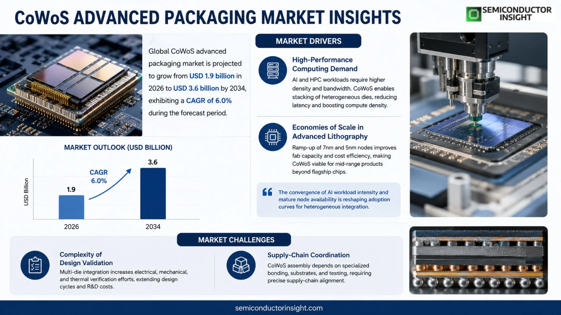
Global CoWoS advanced packaging market size was valued at USD 1.8 billion in 2025. The market is projected to grow from USD 1.9 billion in 2026 to USD 3.6 billion by 2034, exhibiting a CAGR of 6.0% during the forecast period.
CoWoS (Chip‑on‑Wafer‑on‑Substrate) is an advanced heterogeneous integration technique that stacks multiple dies on a silicon interposer before attaching them to a substrate, enabling high‑density interconnects and superior electrical performance for AI accelerators, high‑performance computing and other bandwidth‑intensive applications.
The sector is gaining momentum because AI workloads demand higher compute density while power budgets tighten, prompting designers to adopt CoWoS for its ability to combine logic, memory and specialized processors in a compact form factor. Leading foundries such as TSMC, Intel and Samsung are expanding capacity and offering design incentives, which further fuels adoption across data‑center and edge devices.
MARKET DRIVERS
High‑Performance Computing Demand
Enterprises pursuing AI inference and scientific simulation are pressuring silicon suppliers to deliver density and bandwidth that exceed traditional fan‑out solutions. CoWoS advanced Packaging Market satisfies this need by stacking heterogeneous dies, thereby shortening interconnect paths and slashing latency. Clients that can squeeze more compute per square millimeter gain a competitive edge in data‑center workloads, prompting early adopters to allocate capital toward 2.5‑D integration.
Economies of Scale in Advanced Lithography
Recent ramp‑up of 7 nm and 5 nm process nodes has created surplus capacity in high‑volume fabs, reducing per‑die cost for advanced packaging. When manufacturers align CoWoS processes with mainstream logic production, they capture cost synergies that make the technology financially viable for mid‑range products, not just flagship chips. This cost discipline encourages broader design‑win pipelines across the semiconductor ecosystem.
➤ “The convergence of AI workload intensity and mature node availability is reshaping adoption curves for heterogeneous integration.”
Design houses that embed high‑bandwidth memory (HBM) directly on logic die are now able to meet thermal envelopes without resorting to exotic cooling solutions. This technical advantage reduces time‑to‑market for next‑generation servers, reinforcing the strategic relevance of CoWoS advanced Packaging Market for OEMs seeking differentiation.
MARKET CHALLENGES
Complexity of Design Validation
Integrating multiple dies in a single substrate escalates verification cycles. Engineers must model electrical, mechanical, and thermal interactions across heterogeneous materials, which stretches design schedules and inflates R&D spend. Companies lacking mature simulation tools often face re‑spin risks that erode projected margins.
Other Challenges
Supply‑Chain Coordination
CoWoS assembly relies on a narrow set of specialized bonding facilities. Any disruption,whether from logistical bottlenecks or capacity constraints,creates a ripple effect that can delay product launches across multiple OEMs.
MARKET RESTRAINTS
Capital Intensity of Tooling
Acquiring wafer‑level bonding equipment and precision alignment stations demands multi‑million‑dollar outlays. Smaller fabless firms often lack the balance sheet flexibility to invest, limiting their ability to participate in CoWoS advanced Packaging Market and reinforcing a concentration of capability among a handful of large players.
Regulatory and Environmental Scrutiny
Advanced packaging processes consume atypical chemicals and generate unique waste streams. Emerging environmental regulations in key manufacturing regions impose stricter reporting and remediation requirements, adding compliance costs that can deter new entrants.
MARKET OPPORTUNITIES
Emerging Edge‑AI Devices
Edge devices for autonomous vehicles and smart cameras require compact, high‑throughput compute blocks. CoWoS offers a pathway to embed AI accelerators alongside memory in a miniature footprint, opening a lucrative niche where traditional system‑in‑package (SiP) solutions fall short. Early movers can lock in design‑win agreements with OEMs targeting 2027‑2028 product cycles.
Customizable Interposer Materials
Advances in low‑k dielectric and glass‑based interposers are reducing signal loss while improving thermal dispersion. Companies that develop proprietary interposer stacks can differentiate their offering within CoWoS advanced Packaging Market, capturing premium pricing for performance‑critical applications.
CoWoS Advanced Packaging Market Trends
AI‑Intensive Compute Pressures
CoWoS advanced Packaging Market is reacting to a surge in artificial‑intelligence workloads that demand tighter logic‑to‑memory coupling. Engineers are opting for Chip‑on‑Wafer‑on‑Substrate solutions because they permit dozens of high‑performance dies to share a silicon interposer, trimming interconnect length and curbing signal loss. This architecture directly addresses the power‑budget constraints that modern data‑center accelerators face, allowing designers to meet performance targets without expanding board real estate. The immediate effect is a noticeable shift in design roadmaps: projects that previously relied on discrete components now embed memory, compute, and specialized processors within a single package, yielding a more deterministic thermal profile and faster time‑to‑market.
Other Trends
Foundry Capacity Expansion
Leading silicon foundries are scaling up their CoWoS production lines to match the rising demand. Investment in advanced lithography slots and interposer fabrication has translated into shorter lead times for customers seeking heterogeneous integration. In parallel, design‑win incentive programs encourage early adopters to qualify their IP on the latest process nodes, creating a feedback loop that reinforces capacity builds. This operational scaling not only improves supply reliability but also drives cost efficiencies that make the technology accessible to a broader set of midsized enterprises pursuing edge‑AI solutions.
System‑Level Differentiation Strategies
Manufacturers are leveraging CoWoS to differentiate products at the system level rather than relying solely on raw compute power. By stacking high‑bandwidth memory directly beneath AI cores, chip designers achieve latency reductions that translate into measurable performance gains for inference workloads. The ability to integrate heterogeneous dies also opens pathways for incorporating security enclaves and specialized I/O blocks without incurring additional board complexity. Consequently, product portfolios that embed CoWoS technology can command premium pricing and faster adoption cycles, especially in sectors where latency and power efficiency are decisive factors.
COMPETITIVE LANDSCAPE
Key Industry Players
CoWoS Advanced Packaging Market Competitive Overview
The market is anchored by a handful of large‑scale foundries that have turned CoWoS into a services platform rather than a niche offering. TSMC leads the pack, leveraging its 12‑inch silicon interposer capacity and a suite of design‑for‑CoWoS incentives that lower entry barriers for AI accelerator developers. Intel follows with a vertically integrated approach, pairing its own silicon photonics and advanced packaging fabs to provide end‑to‑end solutions for high‑performance computing clusters. Samsung’s competitive edge lies in its mature backside‑illumination expertise, which it repurposes for high‑bandwidth memory integration on the interposer, allowing customers to meet aggressive power‑per‑performance targets. The trio’s dominance forces smaller players to specialize, either by focusing on niche memory‑centric stacks or by offering ancillary services such as testing, die‑bonding, and substrate engineering.
Beyond the three giants, a constellation of niche but technically proficient firms is shaping the market’s depth. ASE Group and Amkor Technology have expanded their CoWoS‑compatible assembly lines, targeting fabless designers that require rapid turn‑around without the volume commitments demanded by the larger foundries. GlobalFoundries and SMIC, while not yet offering full‑scale interposer production, provide hybrid integration services that combine chip‑on‑wafer capabilities with cost‑effective back‑end processes. European players such as STMicroelectronics and Infineon Technologies concentrate on automotive and industrial applications, where reliability and long‑term supply are prized over raw density. Memory specialists like Micron and NXP contribute by co‑developing HBM‑compatible dies that fit seamlessly onto CoWoS stacks, adding a layer of differentiation for system integrators. This diversified ecosystem creates a competitive pressure that encourages continuous innovation in interposer materials, thermal management, and design automation tools.
List of Key CoWoS Advanced Packaging Companies Profiled
- TSMC
- Intel
- Samsung Electronics
- ASE Group
- Amkor Technology
- GlobalFoundries
- STMicroelectronics
- Infineon Technologies
- Micron Technology
- NXP Semiconductors
- SMIC
- Qualcomm
- IBM
- Applied Materials
- Renesas Electronics
Segment Analysis:
| Segment Category | Sub-Segments | Key Insights |
| By Type |
|
2.5D Interposer is viewed as the foundational approach because it balances integration density with manageable thermal characteristics.
|
| By Application |
|
AI Accelerators dominate the application landscape as designers seek unprecedented compute density.
|
| By End User |
|
Data Center Operators favor CoWoS because it aligns with the need for power‑efficient, high‑throughput modules.
|
| By Technology |
|
Silicon Interposer remains the preferred technology due to its superior electrical characteristics.
|
| By Market Driver |
|
Performance Demands drive adoption as AI workloads push the limits of silicon.
|
Regional Analysis: CoWoS Advanced Packaging Market
Concentrations of 200 mm and 300 mm fabs in Taiwan and Korea host the bulk of CoWoS back‑end activity. These sites leverage mature process control, delivering cost‑effective interposer yields that smaller players struggle to match, thereby reinforcing the region’s dominance in high‑volume production.
Data‑center accelerators and high‑performance networking gear dominate demand, as vendors chase bandwidth advantages offered by silicon‑interposer architectures. The rapid rollout of edge AI devices also nudges tier‑1 chipmakers toward localized CoWoS solutions.
A shift toward vertically integrated supply chains reduces lead times. Foundries are increasingly bundling wafer‑level testing with packaging, a move that mitigates risk for OEMs facing tight product calendars.
Relaxed export controls on advanced packaging equipment in several APAC economies have lowered entry barriers, encouraging new entrants to experiment with multi‑chip‑module designs without heavy compliance overhead.
North America
North America remains a focal point for design innovation, particularly in the United States where major CPU and GPU designers maintain extensive R&D budgets. The region’s strength lies less in wafer output and more in intellectual property generation, fostering collaborations that push CoWoS architectures toward tighter integration with emerging memory technologies. However, the higher cost structure of domestic fabs pushes many firms to outsource production to Asian partners, creating a “design‑first” model that emphasizes system‑level validation over in‑house manufacturing. For service providers, this translates into a growing market for simulation tools and design‑for‑manufacturability consulting.
Europe
European players contribute a nuanced blend of precision engineering and standards‑driven development, especially within the automotive and aerospace sectors where reliability certifications are paramount. While the continent lacks the sheer volume capacity of Asia, its emphasis on quality assurance and compliance opens niches for premium CoWoS solutions tailored to safety‑critical applications. Cross‑border research initiatives, supported by EU funding, also nurture a pipeline of niche technologies such as optical‑interposer hybrids that could redefine connectivity standards.
South America
In South America, market activity revolves around localized assembly and testing services that support regional telecommunications upgrades. The region’s modest domestic fab footprint means most CoWoS components are imported, yet this reliance generates opportunities for value‑added logistics and final‑stage packaging firms that can guarantee rapid turnaround for telecom operators seeking to expand 5G backhaul capacity.
Middle East & Africa
The Middle East & Africa exhibit emerging interest driven by sovereign wealth funds allocating capital toward semiconductor‑related infrastructure. Initiatives to establish “smart city” projects stimulate demand for high‑density compute modules, prompting local consortiums to partner with established CoWoS providers. Although the ecosystem is nascent, the strategic emphasis on digital transformation positions the region as a potential growth frontier for specialized packaging services.
Report Scope
This market research report provides a comprehensive analysis of the CoWoS Advanced Packaging Market , covering the forecast period 2026–2034. It offers detailed insights into market dynamics, technological advancements, competitive landscape, and key trends shaping the industry.
Key focus areas of the report include:
- Market Overview: The report begins with an overview outlining its current market scenario, key growth indicators, and industry transformation drivers. It discusses macroeconomic factors, demand–supply balance, regulatory landscape, and the strategic role of semiconductors in powering advancements across industries such as automotive, telecommunications, consumer electronics, and industrial automation.
- Market Size & Forecast: Historical data and future projections for revenue, unit shipments, and market value across major regions and segments.
- Segmentation Analysis: Detailed breakdown by product type, technology, application, and end-user industry to identify high-growth segments and investment opportunities.
- Regional Insights: Insights into market performance across North America, Europe, Asia-Pacific, Latin America, and the Middle East & Africa, including country-level analysis where relevant.
- Competitive Landscape: Profiles of leading market participants, including their product offerings, R&D focus, manufacturing capacity, pricing strategies, and recent developments such as mergers, acquisitions, and partnerships.
- Technology Trends & Innovation: Assessment of emerging technologies, integration of AI/IoT, semiconductor design trends, fabrication techniques, and evolving industry standards.
- Market Drivers & Restraints: Evaluation of factors driving market growth along with challenges, supply chain constraints, regulatory issues, and market-entry barriers.
- Stakeholder Insights: Insights for component suppliers, OEMs, system integrators, investors, and policymakers regarding the evolving ecosystem and strategic opportunities.
Primary and secondary research methods are employed, including interviews with industry experts, data from verified sources, and real-time market intelligence to ensure the accuracy and reliability of the insights presented.
FREQUENTLY ASKED QUESTIONS:
What is the current market size of CoWoS Advanced Packaging Market?
-> CoWoS advanced packaging market is projected to grow from USD 1.9 billion in 2026 to USD 3.6 billion by 2034, exhibiting a CAGR of 6.0%
Which key companies operate in CoWoS Advanced Packaging Market?
-> Key players include TSMC, Intel, Samsung, GlobalFoundries, and AMD, among others.
What are the key growth drivers?
-> Key growth drivers include rising AI and high‑performance computing workloads, demand for higher compute density under tight power budgets, and the need for heterogeneous integration of logic, memory and specialized processors.
Which region dominates the market?
-> Asia‑Pacific leads the market due to the concentration of leading foundries such as TSMC and Samsung, while North America and Europe also show strong adoption.
What are the emerging trends?
-> Emerging trends include advanced 2.5D/3D stacking, integration of AI accelerators on interposers, and increased design incentives from leading fabs to accelerate CoWoS adoption.

Get Sample Report PDF for Exclusive Insights
Report Sample Includes
- Table of Contents
- List of Tables & Figures
- Charts, Research Methodology, and more...