Advanced Electronic Packaging Materials Market Insights
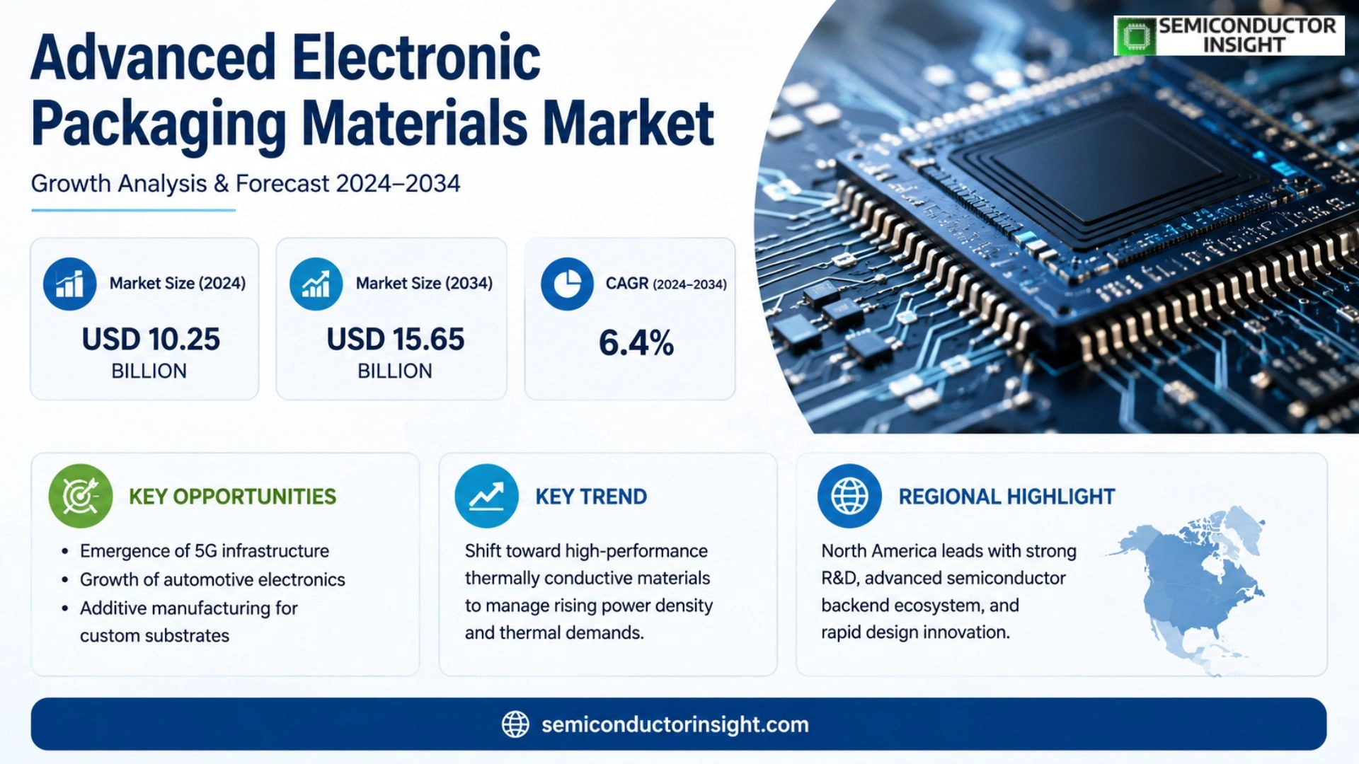
Global Advanced Electronic Packaging Materials market size was valued at USD 10.25 billion in 2024 and will reach USD 15.65 billion by 2034, reflecting a CAGR of 6.4 % over the forecast period.
Advanced Electronic Packaging Materials encompass both electronic packaging and assembly supplies such as potting, encapsulation and plastic packaging compounds, ceramics, glass substrates, solder alloys, electro‑plated metal coatings, bonding agents, printed‑circuit‑board laminates, packaging substrates, adhesives for assembly, low‑k fillers and thermal‑management coatings. The current analysis concentrates on electronic‑grade adhesives and functional film materials.
The upward trajectory stems from expanding semiconductor production,estimated at USD 579 billion in 2022 and expected to climb toward USD 790 billion by 2029,as well as growing demand for high‑performance IoT devices that require reliable thermal management and miniaturized form factors. Companies such as Panasonic, Henkel and Shin‑Etsu MicroSi have announced new high‑temperature adhesive formulations in Q3 2023, while Nitto introduced a low‑dielectric constant film targeting automotive radar modules in early 2024. These initiatives illustrate how material innovators respond to tighter electrical performance specifications and stricter environmental regulations.
MARKET DRIVERS
Miniaturization Pressure Across Device Segments
Manufacturers of smartphones, wearables and IoT sensors are compressing more functionality into ever‑smaller footprints. This push forces Advanced Electronic Packaging Materials Market to supply substrates and interconnects that sustain high signal fidelity while occupying minimal board area. Companies that can deliver low‑dielectric, high‑thermal‑conductivity laminates gain a decisive edge because they enable thinner, lighter products without sacrificing performance.
Shift Toward Heterogeneous Integration
System‑in‑package (SiP) architectures are replacing traditional multi‑chip modules, creating demand for substrates that support mixed‑material stacks, through‑silicon vias and embedded passives. The ability to integrate logic, memory and RF blocks in a single package drives material providers to innovate around thermal management and mechanical reliability. Firms that align their R&D pipelines with these integration trends are positioning themselves for sustained revenue streams.
➤ “Customers prioritize packaging solutions that reconcile thermal constraints with high‑frequency performance, making material differentiation a core competitive factor.”
Supply‑chain resilience also contributes momentum. Recent disruptions highlighted the advantage of diversified material sourcing, prompting OEMs to qualify multiple vendors for critical films and adhesives. This safety‑net approach expands the addressable pool of suppliers, reinforcing overall market activity.
MARKET CHALLENGES
Escalating Cost Structures in High‑Performance Materials
The premium alloys, low‑k polymers and advanced ceramic substrates required for next‑generation packages command price points that exceed traditional PCB materials. While these costs are justified by performance gains, they compress margins for downstream assemblers facing intense price pressure from end‑users.
Other Challenges
Regulatory Compliance Complexity
Stringent RoHS and REACH restrictions limit the use of certain flame retardants and heavy metals, forcing material developers to redesign formulations and re‑qualify processes, which adds time and expense to product launches.
MARKET RESTRAINTS
Technical Barriers to Ultra‑Thin Form Factors
Achieving sub‑100‑micron total thickness while preserving mechanical robustness remains a formidable engineering hurdle. Current bonding agents and dielectric layers can exhibit brittleness at such thinness, leading to yield losses that deter mass adoption of the most aggressive designs.
Moreover, the thermal bottleneck in densely packed dies limits the cooling capacity of conventional heat spreaders. Until reliable, thin‑film thermal interface materials mature, designers may opt for conservative stack‑up configurations, curbing demand for the most advanced offerings.
MARKET OPPORTUNITIES
Emergence of 5G Infrastructure Deployments
Roll‑out of 5G base stations and edge‑computing nodes requires RF‑compatible packaging that tolerates high power density and operates across wide frequency bands. Advanced dielectric films with low loss tangent are essential, creating a niche where material suppliers can capture premium pricing.
Growth of Automotive Electronics
Electric vehicles and ADAS systems increasingly rely on high‑speed data links and power electronics that must endure harsh thermal cycles. Materials engineered for automotive qualification,offering both electrical performance and durability,represent a fast‑growing segment within the overall market.
Finally, the adoption of additive manufacturing for electronic substrates opens a pathway to custom, on‑demand packaging solutions. Early entrants that integrate conductive inks with high‑temperature resins could reshape supply dynamics and capture a share of future design‑for‑manufacturing value.
Advanced Electronic Packaging Materials Market Trends
Shift Toward High‑Performance Thermally Conductive Materials
The relentless push for higher power density in semiconductor devices has forced design houses to re‑evaluate the thermal pathway from chip to board. Traditional silicone‑based compounds are giving way to ceramic and glass‑filled polymers that can ferry heat more efficiently while maintaining electrical isolation. This material migration is not driven solely by technical merit; it reflects a cost calculus where reduced cooling system complexity translates into slimmer form factors and lower assembly labor. Manufacturers that secure a reliable supply of these conductors are poised to capture design wins in data‑center servers, automotive power modules, and emerging 5G infrastructure, where thermal margins are razor‑thin.
Other Trends
Rise of Electronic‑Grade Adhesives for Miniaturization
As component footprints shrink, the adhesive layer becomes a critical structural element rather than a mere filler. Formulations that combine low viscosity with high bond strength enable precise die‑to‑substrate placement without compromising yield. The market is seeing a convergence of adhesive chemistry with under‑fill technologies, allowing manufacturers to address warpage and reliability concerns in stacked‑die architectures. Companies that can deliver a portfolio balancing flexibility, cure speed, and long‑term stability are increasingly sought after by OEMs targeting ultra‑thin smartphones and wearable sensors.
Functional Film Expansion in Flexible Electronics
Flexible displays, roll‑to‑roll photovoltaics, and conformal sensors are expanding the demand for thin‑film materials that combine dielectric strength with mechanical resilience. Polymer‑based functional films are being engineered with nano‑scale fillers that enhance barrier properties while preserving bendability. This evolution is fueled by a surge in IoT deployments where devices must conform to irregular surfaces yet survive harsh environments. Suppliers that integrate printed‑circuit capabilities into these films create a dual‑value proposition,reducing part counts and streamlining assembly lines. Consequently, end‑users are able to accelerate time‑to‑market for products that would have required multiple discrete layers in the past.
COMPETITIVE LANDSCAPE
Key Industry Players
Competitive Pressures and Consolidation in Advanced Electronic Packaging Materials
The market is anchored by a handful of large multinational firms that command a sizable share of revenue and R&D spend. Panasonic continues to leverage its broad semiconductor packaging footprint, pairing its resources in ceramic substrates with aggressive expansion in high‑performance adhesives. Henkel’s specialty chemicals division has deep expertise in electronic-grade adhesives, enabling it to capture premium contracts in automotive and IoT modules. Shin‑Etsu MicroSi’s dominance in silicon‑based plating and advanced encapsulants offers a stable revenue base while it diversifies into functional films for thermal management. The concentration of these three players has fostered a competitive environment where scale, technology patents, and global supply‑chain integration become decisive differentiators for customers seeking reliable, high‑density packaging solutions.
Beyond the tier‑one incumbents, a cohort of specialist manufacturers pursues niche opportunities that collectively shape the market’s breadth. Lord Corp. focuses on low‑k dielectric materials for next‑generation logic chips, while Nitto offers proprietary surface‑treatment chemistries that improve bonding yield. Sumitomo Bakelite’s heritage in high‑temperature resin systems finds relevance in power‑device packaging. Emerging challengers such as Darbond Technology and Huitian New Material target the fast‑growing smart‑terminal segment with innovative potting compounds. Smaller but technically agile firms,including Crystal Clear Electronic Material, Cybrid Technologies, Suzhou Shihua Technology, and several regional players,provide customized solutions that address specific substrate or coating requirements, thereby pressuring larger firms to augment their portfolios through partnerships or targeted acquisitions.
List of Key Advanced Electronic Packaging Materials Companies Profiled
- Panasonic
- Henkel
- Shin‑Etsu MicroSi
- Lord Corp.
- Nitto Denko
- Sumitomo Bakelite
- Darbond Technology
- Huitian New Material
- Crystal Clear Electronic Material
- Cybrid Technologies
- Suzhou Shihua Technology
- Metaforce International
- Taiwan Chem
- Advanced Ceramics Co.
- Formosa Plastics Group
Segment Analysis:
| Segment Category | Sub-Segments | Key Insights |
| By Type |
|
Electronic Grade Adhesives are emerging as the pivotal material class because they enable reliable interconnects in high‑density modules, support diverse substrate chemistries, and tolerate the thermal cycles of advanced packaging processes.
|
| By Application |
|
Integrated Circuit Packaging dominates the application landscape as manufacturers push for higher I/O density and finer pitch interconnects.
|
| By End User |
|
Consumer Electronics drives intense material innovation due to the demand for thinner form‑factors, higher functionality, and robust reliability.
|
| By Material Innovation |
|
Low‑k Dielectric Films are gaining prominence as they reduce parasitic capacitance, enabling faster signal transmission in high‑frequency packages.
|
| By Process Technology |
|
Curing Processes underpin the reliability of advanced packaging by ensuring complete cross‑linking and optimal mechanical properties.
|
Regional Analysis: Advanced Electronic Packaging Materials Market
Silicon Valley, Austin, and the Toronto‑Waterloo corridor operate as clusters where material scientists and packaging engineers co‑develop low‑k dielectrics and anisotropic conductive films, accelerating time‑to‑market for high‑performance devices.
Redundant sourcing strategies, bolstered by near‑shore facilities in Mexico, mitigate disruptions, ensuring consistent material availability for OEMs facing volatile component demand.
Strict RoHS and REACH compliance drives adoption of lead‑free solders and environmentally benign encapsulants, compelling suppliers to certify their formulations across multiple jurisdictions.
Consumer‑driven growth in wearables and IoT devices fuels preference for ultra‑thin, flexible packaging solutions that balance thermal performance with mechanical robustness.
Europe
European manufacturers benefit from a coordinated standards framework that streamlines qualification of novel packaging chemistries. Initiatives such as the EU’s Circular Economy Action Plan incentivize recyclability, prompting the market to experiment with bio‑based substrates and low‑temperature curing processes. While the region lags behind North America in sheer volume, its focus on high‑precision automotive and aerospace applications yields premium segment opportunities for advanced interposers and metal‑based heat spreaders.
Asia‑Pacific
The Asia‑Pacific arena blends expansive consumer electronics production with burgeoning semiconductor fab capacity, especially in Taiwan, South Korea, and Singapore. Local material providers adapt quickly to cost pressures, offering hybrid organic‑inorganic composites that satisfy both price and performance criteria. Rising investment in 5G infrastructure and smart‑city projects amplifies the need for reliable high‑frequency packaging, positioning the region as an emerging growth pole despite ongoing challenges around IP protection.
South America
In South America, Brazil and Mexico serve as regional distribution hubs, yet the market remains under‑penetrated due to limited domestic fab capability. Companies relying on imports are increasingly negotiating long‑term supply agreements to lock in pricing amid currency volatility. Opportunities arise from the region’s expanding renewable‑energy sector, where robust packaging is essential for power‑module reliability in solar‑inverter applications.
Middle East & Africa
The Middle East & Africa market is characterized by selective adoption, primarily driven by defense and aerospace programs in the United Arab Emirates and South Africa. Strategic partnerships with European suppliers enable technology transfer for high‑temperature ceramic substrates. Although overall demand is modest, the focus on mission‑critical electronics creates niche avenues for premium material solutions that can withstand extreme operating environments.
Report Scope
This market research report provides a comprehensive analysis of the Advanced Electronic Packaging Materials Market , covering the forecast period 2026–2034. It offers detailed insights into market dynamics, technological advancements, competitive landscape, and key trends shaping the industry.
Key focus areas of the report include:
- Market Overview: The report begins with an overview outlining its current market scenario, key growth indicators, and industry transformation drivers. It discusses macroeconomic factors, demand–supply balance, regulatory landscape, and the strategic role of semiconductors in powering advancements across industries such as automotive, telecommunications, consumer electronics, and industrial automation.
- Market Size & Forecast: Historical data and future projections for revenue, unit shipments, and market value across major regions and segments.
- Segmentation Analysis: Detailed breakdown by product type, technology, application, and end-user industry to identify high-growth segments and investment opportunities.
- Regional Insights: Insights into market performance across North America, Europe, Asia-Pacific, Latin America, and the Middle East & Africa, including country-level analysis where relevant.
- Competitive Landscape: Profiles of leading market participants, including their product offerings, R&D focus, manufacturing capacity, pricing strategies, and recent developments such as mergers, acquisitions, and partnerships.
- Technology Trends & Innovation: Assessment of emerging technologies, integration of AI/IoT, semiconductor design trends, fabrication techniques, and evolving industry standards.
- Market Drivers & Restraints: Evaluation of factors driving market growth along with challenges, supply chain constraints, regulatory issues, and market-entry barriers.
- Stakeholder Insights: Insights for component suppliers, OEMs, system integrators, investors, and policymakers regarding the evolving ecosystem and strategic opportunities.
Primary and secondary research methods are employed, including interviews with industry experts, data from verified sources, and real-time market intelligence to ensure the accuracy and reliability of the insights presented.
FREQUENTLY ASKED QUESTIONS:
What is the current market size of Advanced Electronic Packaging Materials Market?
-> Advanced Electronic Packaging Materials market will reach USD 15.65 billion by 2034, reflecting a CAGR of 6.4 % over the forecast period.
Which key companies operate in Advanced Electronic Packaging Materials Market?
-> Key players include Panasonic, Henkel, Shin‑Etsu MicroSi, Lord, Nitto, Sumitomo Bakelite, Darbond Technology, Huitian New Material, Crystal Clear Electronic Material, Cybrid Technologies, Suzhou Shihua Technology, among others.
What are the key growth drivers?
-> Key growth drivers include rising demand for electronic‑grade adhesives and functional films, rapid expansion of IoT‑enabled devices, growth of semiconductor manufacturing, and increasing need for advanced thermal management solutions in automotive and consumer electronics.
Which region dominates the market?
-> Asia leads the market, driven by strong semiconductor production hubs in China, Japan, South Korea, and emerging manufacturing in Southeast Asia, while Europe and North America also show significant activity.
What are the emerging trends?
-> Emerging trends include integration of high‑performance electronic‑grade adhesives with functional film technologies, development of eco‑friendly and low‑temperature curing materials, and advanced thermal‑management coatings to support high‑power density applications.

Get Sample Report PDF for Exclusive Insights
Report Sample Includes
- Table of Contents
- List of Tables & Figures
- Charts, Research Methodology, and more...
 Download Sample Report PDF