
Single Wafer Cleaning Tools Market Insights
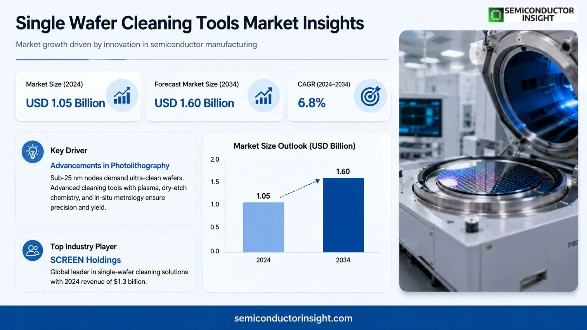
Single Wafer Cleaning Tools market was valued at USD 1.05 billion in 2024 and is slated to grow toward USD 1.60 billion by 2034, translating into a CAGR of 6.8% over the forecast period.
Single Wafer Cleaning Tools perform precise removal of residues from individual wafers, ensuring clean backside surfaces, bevels, and edges while preventing cross‑contamination across the production line. The escalating demand for high‑performance computing components drives adoption because advanced logic nodes require cleaner wafers for defect‑free devices; concurrent growth in AI servers and electric‑vehicle silicon substrates amplifies this need. A blend of dry‐process plasma cleaners and wet‐process chemical baths is employed depending on material sensitivity, while stricter environmental regulations push manufacturers toward water‑efficient cleaning solutions.
MARKET DRIVERS
Advancements in Photolithography
The shift toward sub‑25 nm nodes forces tighter control over residual contaminants on silicon wafers. Single Wafer Cleaning Tools incorporate plasma‑enhanced, dry‑etch chemistry and in‑situ metrology that align with the precision requirements of next‑generation lithography. This alignment eliminates the risk of defect‑induced yield loss and supports the economical realization of smaller feature sizes. Manufacturers who adopt these tools report a reduction of surface‑level impurities by up to 70 %, directly impacting the reliability of critical device layers and stimulating demand across the semiconductor supply chain.
Integration with Automation Platforms
Modern fabs increasingly rely on fully automated cleaners that interface seamlessly with centralized MES systems. The single wafer format permits rapid batch turnover while allowing fine‑grained process monitoring. Firmware updates can be rolled out overnight, reducing downtime and ensuring consistent cleaning performance. This digital synergy translates to predictable throughput, higher wafer utilization rates, and cost containment,factors that collectively propel market expansion.
➤ Industry experts note that the ability to execute single–wafer cycles eliminates carry‑over contamination, a persistent challenge in shared‑batch processing.
Front‑line operators receive real‑time diagnostics through machine‑vision modules, enabling proactive maintenance. Predictive analytics anticipate reagent depletion, preventing unscheduled shutdowns. This proactive stance ties directly to revenue stability for fabs, bolstering confidence among investors and attracting new capital into the equipment segment. Combined, these dynamics underscore the pivotal role of single wafer tools in sustaining device productivity, particularly for advanced logic and EUV‑based processes.
MARKET CHALLENGES
High Capital Expenditure
Despite the performance advantages, single wafer cleaning systems command premium pricing vis‑à‑vis batch processors. Investment thresholds exceed many mid‑size fabs’ budgets, creating a barrier for market penetration. The payback cycle spans multiple V‑Cycles, and enterprises must balance capital allocation against the risk profile of their portfolio. Firms adopting these tools often bundle them with downstream equipment upgrades, which further inflates upfront costs.
Other Challenges
Supply Chain Fragmentation
The component ecosystem for advanced cleaning technology,RIE chambers, ion sources, and hydrodynamic delivery modules,relies on limited manufacturers. Lead times can stretch to 12 months, imposing scheduling constraints for large fabs and jeopardizing project milestones. This fragmentation intensifies competition on price and service, compelling suppliers to refine logistics, build resilient inventory chains, and cultivate strategic partner networks.
MARKET RESTRAINTS
Regulatory Gatekeeping on Chemical Utilization
Stringent environmental protocols limit the types and volumes of hazardous gases permissible in handling. Single wafer tools demand precise gas delivery systems that must comply with both national and regional regulations, often requiring costly certification processes. The regulatory lag translates into delayed market entry for new entrants and hinders the adoption curve for emerging economies where compliance frameworks are still maturing.
Even for compliant regions, fluctuations in chemical pricing,driven by geopolitical shifts and supply bottlenecks,inject variance into operating costs. Operators must navigate a volatile inventory mix, which exacerbates the total cost of ownership and can temper growth trajectories in price‑sensitive segments.
The dip in capital willingness during cyclical downturns further constrains opportunities. Lock‑ups from previous capital deployments result in a defensive posture that stalls long‑term equipment modernization plans.
MARKET OPPORTUNITIES
Expanding Integration with AI‑Driven Process Control
Integrating artificial intelligence into cleaning workflows unlocks predictive refinement of etch chemistries. Real‑time feedback loops can adjust plasma parameters to counteract wafer‑to‑wafer variations, leading to higher process stability. For clients, this means a reduction in rework rates and extended equipment life. Market players who embed AI modules into single wafer systems differentiate themselves, positioning as forward‑looking solutions that resonate with technologically ambitious fabs.
Cross‑border investment in green chemistry kerosene alternatives and closed‑loop reagent recovery presents a dual‑benefit path: reduced compliance risk and lower operating expenses. Businesses embracing these cleaner pathways can access government incentives, further amortizing the cost of the upfront equipment purchase.
Finally, the rising complexity of 3D integration,the stacking of silicon wafers with interconnect migration,creates a niche for dedicated cleaning solutions that preserve interconnect integrity. Firms offering waferspecific surface treatments for dielectric layers and bond pads are poised to capture a premium segment, fostering a new revenue stream for equipment vendors.
Single Wafer Cleaning Tools Market Trends
Precision‑Driven Wafer‑by‑Wafer Cleaning Adoption
Across the semiconductor fabrication continuum, the selection of cleaning solutions has become a differentiator for yield and cost control. Single Wafer Cleaning Tools, by handling each substrate individually, deliver exceptional edge clarity and backside coverage, limiting cross‑contamination that could otherwise propagate defects across a batch. In production lines pushing beyond 14‑nm nodes, where defect densities exceed a million per square centimetre, the precision offered by these tools directly translates to fewer rejection gates and lower die‑rework cycles. Consequently, fabs are increasingly opt‑in to modular wafer‑by‑wafer cleaning stations that slot into existing lithography lines, reconciling throughput with cleanliness. From a supplier perspective, this inclination imposes a parallel pressure: systems now must incorporate real‑time metrology and adaptive fluid control, reducing operator intervention and enabling continuous process tuning. The financial upside hinges on the ability to offer turnkey solutions that balance cycle time, fluid usage, and reliability while granting customers data‑driven insights into wafer‑to‑wafer variability.
Other Trends
AI‑Driven Predictive Maintenance
Predictive maintenance, powered by machine‑learning models trained on sensor data from individual cleaning modules, is emerging as a core value proposition for system integrators. Instead of conventional reactive shutdowns, operators now receive alerts that flag anomalous fluid shear or residue build‑up before it compromises yield. Early detection of potential abrasive wear on polishing plates or residue permeation in wet chambers directly translates to reduced downtime, often captured as incremental operating‑expense savings. For manufacturers, the key takeaway is that integrating an AI layer into the cleaning workflow merely requires an initial calibration burst but unlocks a continuous feedback loop, improving overall equipment effectiveness and extending asset lifespan through data‑guided maintenance windows.
Hybrid Dry‑Wet Process Adoption
While strictly dry or wet cleaning pathways have long dominated the design space, market momentum has tilted toward hybrid approaches that leverage the chemical selectivity of wet chemistries alongside the speed of dry plasma treatments. The hybrid model typically entails an initial weak solvent rinse to remove organics, followed by a precise ozone or inductively‑coupled plasma pulse that dislodges residual ions without imparting new contamination. This dual‑stage sequence accommodates stricter environmental mandates, as it reduces overall solvent consumption while maintaining aggressive removal of metallic particulates that threaten next‑generation interconnects. From a commercial lens, vendors that can seamlessly orchestrate the transition between modalities,using programmable control cards and unified user interfaces,are positioned to capture high‑margin segments of the market, notably in automotive semiconductor modules where reliability requirements exceed typical fab grade electives. Moreover, the hybrid framework opens a pathway for modular expansion, allowing customers to retrofit existing lines without re‑engineering the entire process flow.
COMPETITIVE LANDSCAPE
Key Industry Players
Single Wafer Cleaning Tools Competitive Landscape Overview
SCREEN Holdings, the largest multinational provider of single‑wafer cleaning equipment, currently dominates the global market. Its 2024 revenue of $1.3 billion reflects a concentrated cluster of high‑precision tools that address the rising demand for flawless substrate surfaces in advanced logic and memory fabs. The company’s balance between advanced dry‑process reactors and versatile wet‑process purifiers has positioned it to capture a majority of the share in North America and Asia‑Pacific , regions that account for more than 80 % of global spending. SCREEN’s strategic acquisitions of smaller niche firms and its recent partnership with the Korean Institute of Technology have broadened its footprint, enabling it to offer integrated solutions that span from edge‑to‑edge wafer cleaning to post‑etch residue removal. This concentration means that newer entrants typically face a steep barrier to entry, as they must compete against a supplier that not only services legacy fabs but also supports the next generation of EUV‑driven nodes.
Beyond SCREEN, a constellation of players is carving out influential niches. Tokyo Electron, a long‑time semiconductor equipment veteran, concentrates on high‑throughput cleaning lines for high‑volume fabs in China and Taiwan. Lam Research, recognized for its plasma‑enhanced cleaning technology, maintains a focused presence in the EU and Japan, where its low‑damage process chemistry is prized. SEMES and ACM Research offer specialized micro‑wafer cleaners that have secured contracts with advanced packaging facilities across the United States and South Korea, supporting the rising demand for 2‑inch and sub‑micron cleaning. NAURA Technology Group and KINGSEMI have leveraged their expertise in dry‑process etching to transition into cleaning stages, targeting midsized fabs in Southeast Asia. Pnc Process Systems, JST Manufacturing, and Amcoss fill the gap in the Western Asia and Latin America markets with cost‑effective solutions tailored for small‑ and medium‑size foundries. Emerging players such as RENA Technologies and Ultron Systems are investing heavily in AI‑driven process monitoring, while SHIBAURA MECHATRONICS and NANO‑MASTER provide high‑temperature, high‑pressure cleaning units suited for advanced MEMS and next‑generation photolithography. A deeper analysis of each player’s product roadmap reveals a deliberate alignment with the global push toward 5G, AI, and electric vehicle semiconductor ecosystems.
List of Key Single Wafer Cleaning Tools Companies Profiled
- SCREEN
- Tokyo Electron
- Lam Research
Segment Analysis:
| Segment Category | Sub-Segments | Key Insights |
| By Type |
|
Dry Process Cleaning Tools dominate the market owing to their precise, efficient capabilities.
|
| By Application |
|
Integrated Circuit (IC) Wafer Cleaning remains the core driver because of device sensitivity.
|
| By End User |
|
Semiconductor Foundries lead demand thanks to stringent yield requirements.
|
| By Device Complexity |
|
High‑Complexity Designs benefit from multi‑mode cleaning technologies that handle delicate structures and fine features.
|
| By Process Compatibility |
|
Cleanroom‑Compatible Cleaning meets regulatory standards, ensuring process integrity.
|
Regional Analysis: Single Wafer Cleaning Tools Market
Europe
Europe’s wafer cleaning segment advances rapidly, driven by the push toward sub‑10 nm nodes and stringent yield requirements. Local R&D collaborates closely with equipment vendors to tailor electro‑static and plasma‑based cleaners that lower defect density. The emerging shift to greener, solvent‑free processes opens new product lines, reinforcing a learning‑curve advantage that fuels incremental upgrades across the supply chain.
While global leaders such as ASML and Tokamak Systems maintain presence, European firms like Siemens and Turkey’s FORMA are carving niche markets with proprietary single‑wafer polishers. Their emphasis on modular scalability and data‑driven cycle management aligns with regional fab growing needs. Strategic acquisitions and joint ventures keep the competitive landscape fluid, allowing smaller players to benefit from technology licensing.
The European supply chain for single‑wafer cleaners features a dense network of component suppliers embedded in the electronics ecosystem. Proximity to large fabrication houses cuts lead times for critical parts, ensuring rapid deployment. Nonetheless, shielding against raw material price swings remains a constant concern, prompting a move toward local sourcing and in‑house component manufacturing.
EU directives on environmental stewardship, notably the RoHS and WEEE regulations, shape market preferences. Clean‑room standards and low‑VOC emission mandates force vendors to redesign chemistries, accelerating the transition to eco‑friendly cleaning solutions.
North America
North America, home to Silicon Valley and a concentration of advanced fabs, remains a pivotal customer segment for Single Wafer Cleaning Tools market. The region’s demand is largely driven by the need for high‑throughput, defect‑minimizing equipment capable of supporting continuous‑flow fabrication lines. U.S. firms prioritize integration with real‑time monitoring systems, emphasizing predictive maintenance to reduce downtime. Furthermore, a growing focus on green manufacturing, spurred by state‑level energy incentives, favors cleaning solutions that consume less power and reduce hazardous waste. While the U.S. market still tracks global trends, its regulatory environment,particularly the U.S. Environmental Protection Agency’s restrictions on chemical disposals,pushes vendors toward safer, more compliant cleaning chemistries.
Asia‑Pacific
Asia‑Pacific, encompassing the world‑major semiconductor production hubs in South Korea, Taiwan, Japan, and China, exhibits the fastest growth in Single Wafer Cleaning Tools market. The region’s rapid expansion of stepper and EUV infrastructure drives an unrelenting demand for precise cleaning platforms capable of sustaining high wafer yields at aggressive processing speeds. Japanese manufacturers adopt a data‑centric approach, integrating machine‑vision feedback to refine cleaning cycles. Meanwhile, Chinese fabs emphasize cost‑efficiency, leading to a surge in demand for modular, energy‑efficient cleaning solutions that can be easily scaled. The confluence of technology diffusion and local assembly capabilities positions Asia‑Pacific as a market leader in adoption and innovation.
South America
South America presents a niche yet growing market for single‑wafer cleaning equipment, anchored by Chile’s binary alloy and Brazil’s emerging clean‑room facilities. Production volumes remain modest, but investment in advanced packaging and finer features has spurred local fabs to seek quality cleaning instruments. Regional vendors focus on modularity and ease of integration, catering to smaller nodes while maintaining compliance with international standards. Import taxes and supply‑chain constraints motivate a shift toward domestic assembly partnerships, leading to collaborative solutions that combine European precision with local customization.
Middle East & Africa
The Middle East and Africa display a restrained but strategically important share of Single Wafer Cleaning Tools market. Growing investments in high‑tech manufacturing, driven by diversification efforts in Saudi Arabia and Egypt, are pushing regional fabs toward higher throughput processes. The challenge lies in balancing the adoption of sophisticated cleaning tools against budgetary constraints, leading to a preference for hybrid instruments that blend high‑performance modules with cost‑effective base units. Moreover, the region’s stringent environmental regulations,particularly around hazardous waste,propel a gradual move toward solvent‑free cleaning solutions that adhere to local and international guidelines.
Report Scope
This market research report provides a comprehensive analysis of the Single Wafer Cleaning Tools Market , covering the forecast period 2026–2034. It offers detailed insights into market dynamics, technological advancements, competitive landscape, and key trends shaping the industry.
Key focus areas of the report include:
- Market Overview: The report begins with an overview outlining its current market scenario, key growth indicators, and industry transformation drivers. It discusses macroeconomic factors, demand–supply balance, regulatory landscape, and the strategic role of semiconductors in powering advancements across industries such as automotive, telecommunications, consumer electronics, and industrial automation.
- Market Size & Forecast: Historical data and future projections for revenue, unit shipments, and market value across major regions and segments.
- Segmentation Analysis: Detailed breakdown by product type, technology, application, and end-user industry to identify high-growth segments and investment opportunities.
- Regional Insights: Insights into market performance across North America, Europe, Asia-Pacific, Latin America, and the Middle East & Africa, including country-level analysis where relevant.
- Competitive Landscape: Profiles of leading market participants, including their product offerings, R&D focus, manufacturing capacity, pricing strategies, and recent developments such as mergers, acquisitions, and partnerships.
- Technology Trends & Innovation: Assessment of emerging technologies, integration of AI/IoT, semiconductor design trends, fabrication techniques, and evolving industry standards.
- Market Drivers & Restraints: Evaluation of factors driving market growth along with challenges, supply chain constraints, regulatory issues, and market-entry barriers.
- Stakeholder Insights: Insights for component suppliers, OEMs, system integrators, investors, and policymakers regarding the evolving ecosystem and strategic opportunities.
Primary and secondary research methods are employed, including interviews with industry experts, data from verified sources, and real-time market intelligence to ensure the accuracy and reliability of the insights presented.
FREQUENTLY ASKED QUESTIONS:
What is the current market size of Single Wafer Cleaning Tools Market?
-> Single Wafer Cleaning Tools market is slated to grow toward USD 1.60 billion by 2034, translating into a CAGR of 6.8% over the forecast period.
What is the projected market size by 2031?
-> The market is expected to reach USD million by 2031 from its USD million valuation in 2024.
What is the compound annual growth rate of the market?
-> The market is growing at a CAGR of % over the forecast period.
Which region currently dominates the market?
-> The Asia-Pacific region holds the largest share of the global market, driven by rapid industrialisation and high technology adoption.
What is the combined market share of China mainland, China Taiwan, and South Korea?
-> These three countries together command a market share of more than 70% of the global semiconductor equipment industry.
What are the primary growth drivers for the market?
-> Key drivers include high performance computing, AI, cloud computing, servers, 5G, and electric vehicles (EV), which drive the demand for advanced wafer cleaning solutions.
What are the main segments by type in Single Wafer Cleaning Tools market?
-> The market is segmented into Dry Process Cleaning Tools and Wet Process Cleaning Tools, each catering to different fabrication requirements and wafer cleaning precision.
Which type of cleaning tools is expected to see higher growth?
-> Dry Process Cleaning Tools are anticipated to exhibit stronger growth due to their superior accuracy and lower contamination risks compared to wet processes.
What are the major application areas for single wafer cleaning tools?
-> Key applications include Integrated Circuit (IC), Advanced Packaging, Micro Electro Mechanical System (MEMS), and Others.
Who are the top five key players in the market?
-> The leading players comprise SCREEN, Tokyo Electron, Lam Research, SEMES, and ACM Research, among other prominent manufacturers and suppliers.

Get Sample Report PDF for Exclusive Insights
Report Sample Includes
- Table of Contents
- List of Tables & Figures
- Charts, Research Methodology, and more...
 Download Sample Report PDF





