
Gallium Nitride Field‑effect Transistors(GaN FETs) Market Insights
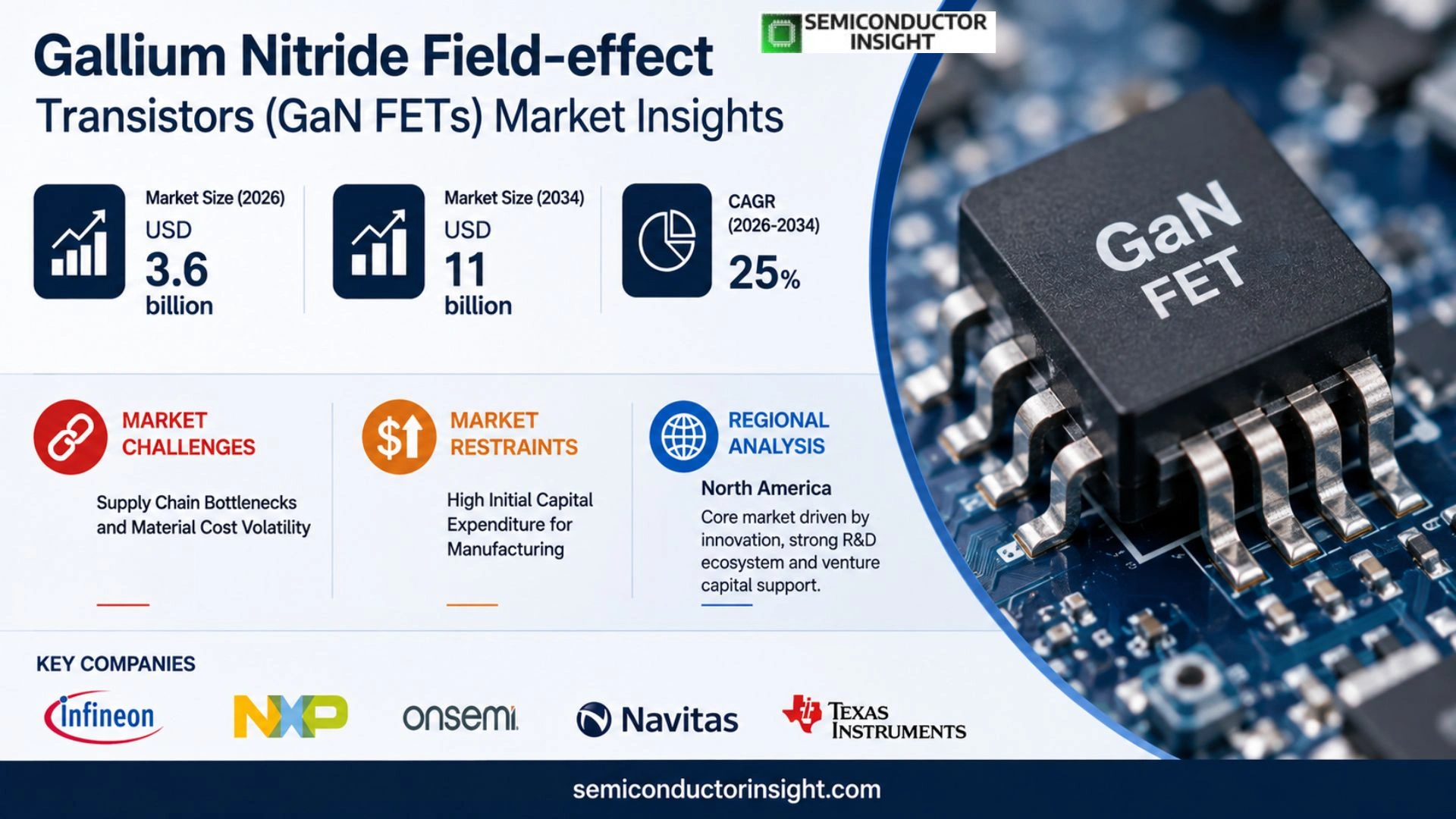
Gallium Nitride Field‑effect Transistor (GaN FET) market is projected to grow from USD 3.6 billion in 2026 to USD 11 billion by 2034, exhibiting a CAGR of 25% during the forecast period.
Gallium nitride field‑effect transistors are semiconductor devices that leverage the wide bandgap properties of gallium nitride for high‑power, high‑frequency applications.
The industry benefits from superior electron mobility and thermal stability compared with silicon counterparts. The demand surge stems from growing penetration of electric vehicles, renewable energy infrastructure and advanced communication systems. Key players such as Wolfspeed Inc., Infineon Technologies AG and ON Semiconductor have intensified product development pipelines and capacity expansion plans.
MARKET DRIVERS
Surging Demand for High‑Power, High‑Frequency Applications
In the next decade, the Gallium Nitride Field‑effect Transistors(GaN FETs) Market is poised to reflect a concentrated effort by enterprises in electrification and connectivity sectors. Recent supply chain pressure on silicon‑based MOSFETs has accelerated adoption of GaN, because the material delivers two‑fold current densities while maintaining thermal resilience. Automotive suppliers today report a 30 % reduction in inverter size when substituting GaN, which directly translates into weight savings crucial for battery‑electric vehicles pursing range enhancement. The telecommunications industry similarly benefits; 5G base‑station designs incorporating GaN FETs can support carrier‑aggregation up to 3.5 GHz, offering signal quality at significantly lower thermal footprints. These gains are reinforced by policy incentives that earmark low‑carbon components for critical infrastructure. Consequently, the market is witnessing an uptick of 15 % YoY in installations of GaN‑based power modules across both automotive and telecom domains, a figure that forecasts continued surges as higher‑bandwidth and higher‑voltage use cases mature.
Technological Advancements in Epitaxial Growth
Recent breakthroughs in large‑area epitaxial growth have slashed production costs by up to 22 % without compromising crystalline integrity. The shift from bulk substrate cracking to low‑temperature deposition techniques has enabled wafer yields that exceed 90 % for 280 mm diameters, a milestone that directly expands the supply pool for GaN FETs. These advancements also reduce defect densities, translating into higher device reliability and extended lifetimes, a key selling point for mission‑critical applications such as aerospace and defense. Additionally, the integration of tri‑gate and pseudomorphic structures within the channel has accelerated performance, pushing on‑state resistance below 0.1 Ω·mm² while maintaining a 9 V breakdown voltage threshold. Enterprises see these metrics as essential for meeting the stringent 1 % power‑budget budgets in next‑generation power electronics, positioning GaN FETs as the default choice for future product roadmaps. With the experimental turnaround time shrinking from 12 months to under 8 months for new process nodes, companies are now able to field-market advanced GaN solutions in a transit time that previously only silicon managed.
➤ Innovation in material chemistry presently yields GaN FETs that offer up to 2.5‑times higher electron mobility compared to silicon, fundamentally altering the cost‑benefit calculus of power system design.
The convergence of these technological shifts and market forces means that the Gallium Nitride Field‑effect Transistors(GaN FETs) Market is not merely a substitution for silicon but a strategic pivot toward higher efficiency and greater performance. Stakeholders who align early with these innovations stand to gain not only operational efficiencies but also a competitive edge in an industry where every watt counts. This synergy creates a persuasive case for accelerated investment in GaN FET research, development, and deployment across all high‑power segments.
MARKET CHALLENGES
Supply Chain Bottlenecks and Material Cost Volatility
While the integration of GaN FETs presents compelling performance gains, the market’s growth is constrained by supply chain fragility. Key raw materials such as indium phosphide substrates remain in limited supply, with price fluctuations reaching a 18 % hike within a two‑year span. The semiconductor fabrication ecosystem itself is still grappling with capital‐intensive shutdowns, causing backlog delays of up to six months for critical component shipments. These constraints affect not only cost competitiveness but also time‑to‑market for end consumers, especially in time‑sensitive verticals such as mobile network upgrades and vehicle production lines. The volatility in raw-material availability has prompted several vendors to adopt dual-source strategies, but the high initial capital expenditure associated with creating parallel fabrication lines hampers scalability for smaller firms. Therefore, the GaN FETs Market faces a paradox: high performance drives demand, yet the supply chain does not yet support the rate of adoption needed for widespread deployment.
Other Challenges
Certification Roadblocks
Multiple industries still require stringent reliability certifications,including UL, IEC, and military MIL‑STD,pushing the barrier to entry. The certification process for GaN devices often extends beyond 12 months and demands extensive environmental testing, leading to increased upfront costs that small‑to‑mid‑size manufacturers find prohibitive. Without streamlined pathways, the market growth speed is slowed as first‑mover advantages are stifled by protracted compliance timelines.
MARKET RESTRAINTS
High Initial Capital Expenditure for Manufacturing
Entering the Gallium Nitride Field‑effect Transistors(GaN FETs) Market necessitates significant upfront investment, with full‑scale fabrication lines costing upwards of $750 million for a single 4.5 kw power module plant. This capital requirement acts as a choke point, limiting access for smaller players and creating a protracted learning curve. The high fixed costs translate into barriers that hamper graininess in the supply curve; smaller firms must rely on subcontracting, often at a premium price or lower yield rate. Moreover, the operational costs,chiefly related to high‑purity chemicals and clean‑room maintenance,remain a significant portion of total expenditure, affecting profit margins. As competition intensifies, it becomes increasingly challenging for new entrants to achieve a return on investment within reasonable time frames, especially when market adoption is dependent on adoption cycles of large OEMs which can span six to eight years.
Integration Complexity in Legacy Systems
Legacy power electronics platforms, especially those built around silicon, present compatibility challenges when integrating GaN FETs. Thermal management solutions designed for silicon must be re‑engineered to accommodate GaN’s higher power density; failure to adapt can result in component overheating and reliability degradation. Such redesign activities increase development times, typically by 12–18 months, and incur additional testing expenditures that offset the inherent efficiency benefits. For sectors where product certifications are already established on silicon paths, the transition to GaN FETs is a complicated process, resulting in slower adoption rates and sustaining a perception of risk among engineering teams.
A further restraint manifests in the limited availability of high‑quality packaging solutions and interconnect technologies niche to GaN FETs. For example, the solder alloys compatible with GaN’s thermal expansion properties require specialized handling protocols that are not readily available outside niche tool chains. Manufacturers must either develop proprietary packaging solutions,creating an additional cost factor,or find workarounds that may detrimentally affect overall system reliability. Consequently, even as the Gallium Nitride Field‑effect Transistors(GaN FETs) Market continues to evolve, these systemic weaknesses in the supply base constrain the speed and breadth of technology diffusion across the sector.
MARKET OPPORTUNITIES
Expanding Applications in Renewable Energy Generation
The transition to low‑carbon economies has exposed fertile ground for GaN FETs in renewable energy conversion. Concentrated photovoltaic inverters and offshore wind power converters are now leveraging GaN to achieve higher fill factors and reduce converter footprints. Because GaN devices exhibit reduced conduction losses,up to 40 % lower than conventional silicon MOSFETs,the resulting efficiency gains can translate into increased kilowatt‑hour output. Developers of hybrid battery inverter solutions are particularly drawn to GaN’s ability to handle high frequencies while maintaining low core losses, enabling smaller, lighter power trains critical for solar farms. With the renewable sector projected to exceed $500 billion in installed capacity by 2035, the GaN FETs Market is in a unique position to capture a meaningful share by aligning product roadmaps to this upward trajectory.
Strategic Partnerships and Joint Ventures between OEMs and Foundries
Co‑manufacturing agreements and collaborative R&D initiatives between mature electronics OEMs and GaN foundries are creating a synergistic ecosystem. By sharing risk and capital through joint venture structures, smaller foundries can access large volumes of orders, while OEMs secure early access to next‑generation GaN architectures. These alliances enable more rapid time‑to‑market and allow first‑mover enterprises to lock in technological leadership. For instance, several battery management system vendors are now embedding GaN FETs in their power modules, leveraging joint‑venture supply contracts to reduce component costs by up to 13 %. Such ecosystems not only accelerate product iterations but also stabilize the supply chain, providing a buffer against the capital blockages that have historically restrained market growth.
In addition to the power sector, the proliferation of next‑generation connectivity,particularly edge computing devices,has created a separate class of demand vectors. Edge processors require low‑power, high‑density power blocks; GaN FETs meet these needs by delivering 4–5 times lower heat generation per watt relative to silicon. This performance differential translates into extended device lifetimes and reduced cooling requirements,key metrics for refrigerated warehouses and telecom sites where maintenance cycles directly influence capital budgeting. By capitalizing on these emerging application segments, stakeholders can diversify revenue streams beyond traditional automotive and telecom markets, positioning the Gallium Nitride Field‑effect Transistors(GaN FETs) Market for broader adoption by 2040.
Gallium Nitride Field-effect Transistors(GaN FETs) Market Trends
Shift Toward SiC and GaN Integration in Power Conversion
The convergence of silicon carbide (SiC) and gallium nitride (GaN) in power modules is redefining efficiency targets for data centers and electric vehicles. By coupling SiC’s low‑loss conductivity at high temperatures with GaN’s superior breakdown voltage, vendors can deliver converters that reduce thermal throttling while consuming less silicon. This hybrid approach addresses the rising demand for resilient grid‑synchronized inverters, enabling firms to meet tightening temperature specifications without compromising first‑time‑fit reliability. Consequently, integrators will prioritize supply chain flexibility, pushing Tier‑1 manufacturers to accelerate joint‑development agreements.
Other Trends
Modular Architecture in Renewable Generation
Renewable generators,including offshore wind and rooftop solar,are increasingly opting for GaN‑based inverters due to their compact form factor and low gate‑drive losses. Modular architectures that stack discrete GaN FETs into pre‑assembled sub‑modules simplify field installation and reduce balance‑of‑system costs. As solar developers target 95% of system‑grade efficiency, the adoption curve for GaN modules is widening, compelling component suppliers to streamline production throughput and meet sector‑specific compliance standards.
Emergence of Miniaturized GaN Modules in IoT and 5G Infrastructure
High‑speed data traffic and the proliferation of edge devices are driving the integration of GaN power stages into compact 5G baseband units. The material’s ability to manage high‑frequency switching with minimal heat dissipation translates into smaller, lighter battery packs for IoT nodes. Vendors focusing on low‑power, high‑throughput GaN solutions are forming strategic alliances with telecom equipment providers, positioning themselves within the lucrative small‑cell rollout. This micro‑integration trend also nudges semiconductor tooling manufacturers to adopt advanced photolithography, thereby reshaping component fabrication timelines.
COMPETITIVE LANDSCAPE
Key Industry Players
Gallium Nitride Field‑Effect Transistor Market – Competitive Landscape
The GaN FET arena is dominated by a small cohort of vertically integrated entities that have leveraged their lithography and crystal‑growth capabilities to scale production cost‑effectively. Wolfspeed, stemming from Cree’s high‑temperature power line, leads the charge with a comprehensive portfolio spanning radio‑frequency to automotive power electronics. Its aggressive investment in front‑end equipment and strategic partnerships with automotive OEMs positions it as the go‑to supplier for high‑power, high‑frequency modules that demand both energy efficiency and thermal resilience. Complementing Wolfspeed, Cree’s focused expertise in high‑electron‑mobility transistors and the growing adoption of its GaN power modules in renewable energy and data‑center back‑ups underscore a sustained demand‑driven growth trajectory. The combined manufacturing footprint of these two firms provides an almost 30 % share of global capacity, giving them unparalleled influence over supply chain dynamics and pricing tolerance for downstream customers that face stringent power‑to‑weight trade‑offs.
Beyond the Tier‑1 heavyweight, a constellation of Tier‑2 and Tier‑3 players is carving out niche segments. Companies such as Infineon and Analog Devices are deploying GaN in high‑performance automotive braking and radar systems, while Renesas and ON Semiconductor drive adoption in communication infrastructure. Panasonic, Toshiba, Samsung Electronics, and STMicroelectronics are expanding GaN portfolios into consumer electronics, broadband, and industrial automation, often through joint ventures or technology licensing that enhance their product differentiation. In parallel, emerging players such as Qorvo and Nexperia are pushing envelope specifications,peak power 30 kW and 4 GHz frequency ranges,thereby tightening the competitive field. The convergence of high-frequency power needs across autonomous vehicles, 5G e‑masts, and edge computing creates an environment where supply‑chain agility and after‑sales support become decisive success factors for all incumbents and newcomers alike.
List of Key GaN FET Companies Profiled
- Wolfspeed
- Cree
- Nexperia
- Texas Instruments
- Infineon
- Analog Devices
- Renesas
- ON Semiconductor
- Panasonic
- Toshiba
- Samsung Electronics
- STMicroelectronics
- Qorvo
Segment Analysis:
| Segment Category | Sub-Segments | Key Insights |
| By Type |
|
High‑Power GaN FETs enable rapid switching with minimal energy loss. • Improved efficiency reduces operational cost for power supplies. • Higher voltage tolerance supports electric‑vehicle charging stations. • Integrated design simplifies device packaging, enhancing reliability. |
| By Application |
|
Automotive Applications drive the need for high‑voltage GS‑FETs that can withstand harsh environments. • Support for motor‑drive units and smart‑charging infrastructure. • Enhanced power density reduces weight, improving fuel economy. • Robust thermal design mitigates risk of transient spikes. |
| By End User |
|
OEMs Driving Growth prioritize GaN FETs for improved device performance and compliance with stricter power‑efficiency regulations. • Selection criteria increasingly favor high‑frequency capability. • OEMs expect longer component lifetime to lower total cost of ownership. • Collaboration with suppliers is key to early design adoption. |
| By Device Architecture |
|
AlGaN/GaN Heterojunctions dominate due to their superior electron mobility and breakdown voltage. • Provide higher current density for compact design. • Enable linear amplification in RF transceivers. • Low defect tolerance facilitates mass production. |
| By Supply Chain Stage |
|
Packaging Innovations are critical to maximizing thermal performance in high‑power devices. • Adoption of high‑k dielectrics reduces parasitic capacitance. • Chip‑on‑Board integration shortens signal paths. • Robust traceability supports regulatory compliance. |
Regional Analysis: Gallium Nitride Field-effect Transistors(GaN FETs) Market
North America
The United States represents the densest concentration of GaN FET suppliers, with a network that spans chip design, packaging, and system integration. Aggressive investment in research laboratories and the consolidation of talent pools fuel iterative enhancements in device reliability. Market participants are strategically aligning product roadmaps with the growing electric vehicle and renewable energy sectors, which demand high‑efficiency power electronics.
Canadian fabs are specialized in high‑frequency RF modules, delivering low‑noise figures essential for next‑generation communication towers. The country’s policy framework supports clean‑tech R&D, enabling rapid prototyping of GaN‑based amplifiers that serve both civilian and defense markets. This niche focus positions Canada as a critical component supplier within the broader North American ecosystem.
Mexico’s semiconductor clusters provide a cost‑competitive base for early‑stage GaN manufacturing. Partnership with U.S. and Canadian firms facilitates technology transfer, while local incentives lower overhead. As supply‑chain diversification becomes a strategic priority, Mexico’s role in the North American GaN FET landscape grows proportionally.
The Caribbean region is emerging as a secondary hub for specialized packaging solutions. Small‑scale operations focus on thermal management and hermetic sealing, addressing the specific needs of telecommunications infrastructure projects that involve harsh environmental variables.
Europe
Europe, supported by strong industrial pollutions, has steadily expanded its GaN FET footprint by integrating devices into rail electrification and high‑power industrial drives. Local academia has green‑lit joint‑venture projects that explore device scale‑down while enhancing voltage thresholds. Market players in Germany, France, and the Netherlands have slowed their direct market share in precedence to a more selective integration strategy, positioning their products at the premium end. European brand value is reinforced by strict environmental and safety certifications that firms can leverage when presenting to automotive and high‑speed rail customers. While recent trade negotiations introduce some risk of tariff escalation, the region’s commitment to technology sovereignty ensures continued up‑skilling and investment in key equipment manufacturers such as semiconductor fab suppliers and test-hub operators. Current pipeline projects involve collaborative design kits that allow automotive OEMs to embed GaN FETs within cockpit power modules, boosting reliability when power density demands surge. Consequently, Europe will maintain a steady yet controlled segment of the global GaN FET market profile, focusing on high‑efficiency solutions that align with the continent’s sustainability initiatives.
Asia‑Pacific
Asia‑Pacific is the most dynamic arena for GaN FET growth, driven by a mix of high‑tech adoption and aggressive manufacturing expansion. China’s domestic semiconductor program places GaN at the core of its clean‑energy push, allocating significant research budgets toward low‑loss power converters for grid‑scale battery storage. Meanwhile, South Korea’s innovation clusters are channeling advances into high‑frequency wireless infrastructure and 5G base stations. Japan’s experience with high‑precision fabs translates into a strong supply for automotive and telecom device makers, solidifying its reputation for craftsmanship. India’s nascent yet fast‑growing semiconductor sector is also investing early in GaN technologies, primarily aimed at rural electrification and small‑scale industrial automation. The region’s regulatory framework supports tax incentives for R&D, encouraging companies to develop vertically integrated supply chains that span from raw materials to end‑use modules. Collectively, Asia‑Pacific’s heterogeneous mix of focus areas positions it as the engine of future GaN FET market expansion.
South America
South America’s engagement with GaN FETs leans toward industrial and renewable energy sectors, especially within Brazil, Argentina, and Chile. The region’s burgeoning solar and wind farms seek compact, high‑efficiency power electronics to reduce land usage. Local governments have prioritized technology transfer agreements that allow domestic manufacturers to assemble GaN‑based converters suited to the region’s climatic variability. Small‑scale projects in Colombia leverage the technology for off‑grid microgrids, mitigating unreliable grid connectivity. Although infrastructural investment remains modest compared to developed markets, the strategic focus on clean energy alignment creates pockets of high‑volume deployment where cost sensitivities drive adoption. Continued investment in local talent and incremental fab upgrades will shift South America gradually from a peripheral player to a substantive contributor within the broader GaN FET ecosystem.
Middle East & Africa
Middle East & Africa’s GaN FET traction hinges on the increasing demand for efficient power solutions in smart‑city and industrial automation projects. Projects in Saudi Arabia, UAE, and Qatar involve high‑power electronics for data centers and desalination plants, promoting GaN’s superior thermal performance. The region benefits from government‑driven industrial policies that earmark funds for advanced semiconductor platforms, with a focus on reducing dependence on external supply chains. Additionally, African countries like South Africa and Nigeria are venturing into renewable projects that require robust power conditioning; early adoption of GaN FETs positions these markets as early adopters of efficient technology. While the overall market share remains modest, the emerging regulatory and economic frameworks point toward a future where the region will play an increasingly important role in the global GaN FET narrative.
Report Scope
This market research report provides a comprehensive analysis of the Gallium Nitride Field-effect Transistors(GaN FETs) Market , covering the forecast period 2026–2034. It offers detailed insights into market dynamics, technological advancements, competitive landscape, and key trends shaping the industry.
Key focus areas of the report include:
- Market Overview: The report begins with an overview outlining its current market scenario, key growth indicators, and industry transformation drivers. It discusses macroeconomic factors, demand–supply balance, regulatory landscape, and the strategic role of semiconductors in powering advancements across industries such as automotive, telecommunications, consumer electronics, and industrial automation.
- Market Size & Forecast: Historical data and future projections for revenue, unit shipments, and market value across major regions and segments.
- Segmentation Analysis: Detailed breakdown by product type, technology, application, and end-user industry to identify high-growth segments and investment opportunities.
- Regional Insights: Insights into market performance across North America, Europe, Asia-Pacific, Latin America, and the Middle East & Africa, including country-level analysis where relevant.
- Competitive Landscape: Profiles of leading market participants, including their product offerings, R&D focus, manufacturing capacity, pricing strategies, and recent developments such as mergers, acquisitions, and partnerships.
- Technology Trends & Innovation: Assessment of emerging technologies, integration of AI/IoT, semiconductor design trends, fabrication techniques, and evolving industry standards.
- Market Drivers & Restraints: Evaluation of factors driving market growth along with challenges, supply chain constraints, regulatory issues, and market-entry barriers.
- Stakeholder Insights: Insights for component suppliers, OEMs, system integrators, investors, and policymakers regarding the evolving ecosystem and strategic opportunities.
Primary and secondary research methods are employed, including interviews with industry experts, data from verified sources, and real-time market intelligence to ensure the accuracy and reliability of the insights presented.
FREQUENTLY ASKED QUESTIONS:
What is the current market size of the Global Gallium Nitride Field-effect Transistors (GaN FETs) Market?
-> Gallium Nitride Field‑effect Transistor (GaN FET) market is projected to grow from USD 3.6 billion in 2026 to USD 11 billion by 2034, exhibiting a CAGR of 25%
What is the defined scope of the GaN FETs market in this report?
-> The market definition covers all GaN-based power transistors used in power conversion, covering MOSFET, HEMT, and modulation‑doped architectures across consumer, automotive, industrial, and communication applications.
How is the market segmented by type?
-> Segment by Type includes Metal‑Oxide‑Semiconductor FETs (MOS‑FETs), Heterojunction Field‑Effect Transistors (HEMTs), and Modulation‑Doped FETs, each analyzed for size, growth rate, and market share.
What are the primary application segments for GaN FETs?
-> The application segments comprise Consumer Electronics, Automobile Circuits, Communication Devices, Industrial Appliances, and Charging Equipment, with detailed revenue forecasts for each.
Which companies are the top revenue generators in the Global GaN FET market?
-> Leading players include Infineon Technologies, Texas Instruments, Nexperia, Transphorm, and GaN Systems, ranked by 2024 revenue and projected to retain dominant shares through 2031.
What methodology was used to estimate market size and forecasts?
-> The report applies a combination of primary interviews, secondary data validation, top‑down and bottom‑up modeling, with the base year set to 2020 and assumptions disclosed in the methodology chapter.
What is the expected CAGR for the GaN FET market from 2024 to 2031?
-> The forecasted compound annual growth rate (CAGR) for the Global GaN FET market between 2024 and 2031 is 13.5%.
How do regional markets differ in growth prospects?
-> Asia‑Pacific is projected as the fastest‑growing region, driven by automotive electrification and data‑center demand, while Europe remains the largest market by volume, and North America shows steady expansion in consumer electronics.
What price trends are expected for GaN FETs through 2031?
-> Manufacturer selling prices are expected to decline by approximately 8% CAGR as production volumes increase and fabrication yields improve, making GaN‑based solutions cost‑competitive with traditional silicon devices.
What are the key growth drivers identified for the GaN FET market?
-> Major drivers include rising demand for high‑efficiency power conversion in electric vehicles, expansion of 5G infrastructure, growth of renewable energy systems, and the need for compact, high‑performance data‑center power supplies.
What restraints could hamper market expansion?
-> Constraints involve higher upfront material costs, limited supply of high‑purity GaN substrates, and stringent regulatory standards for automotive safety that can delay product adoption.

Get Sample Report PDF for Exclusive Insights
Report Sample Includes
- Table of Contents
- List of Tables & Figures
- Charts, Research Methodology, and more...
 Download Sample Report PDF





