635nm-1310nm TO Packaged Laser Diode Market Insights
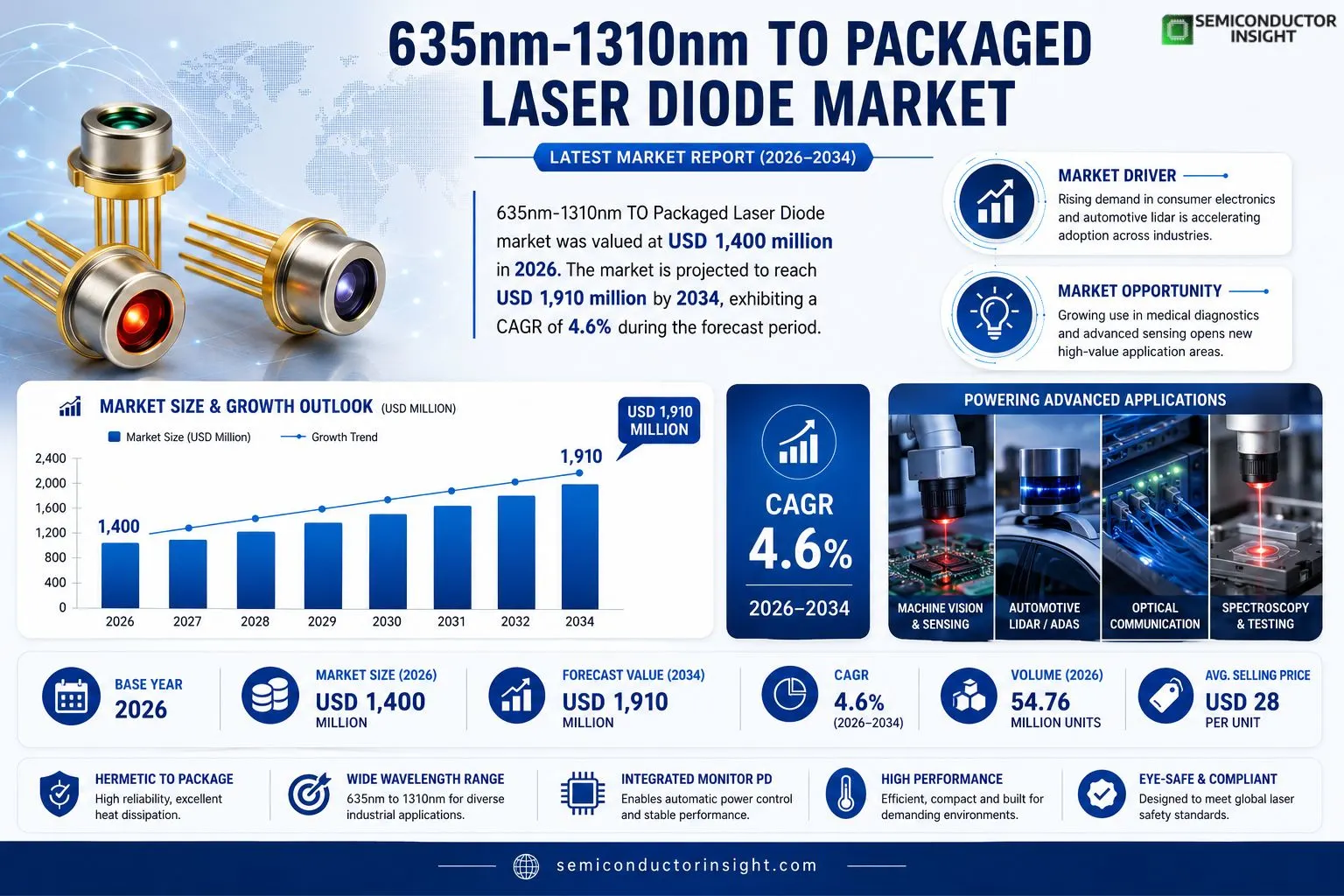
635nm-1310nm TO Packaged Laser Diode market size was valued at USD 1,400 million in 2026. The market is projected to reach USD 1,910 million by 2034, exhibiting a CAGR of 4.6% during the forecast period.
635nm-1310nm TO‑packaged laser diodes are semiconductor lasers that emit wavelengths from visible red (635 nm) through the near‑infrared band (1310 nm). The chips are sealed in a metal‑can (TO) package that provides hermetic protection, electrical connection via a metal base/pin and efficient heat dissipation; the top cap may incorporate a transparent window or collimating lens, and some variants embed a monitoring photodiode for automatic power control (APC). In 2026 production reached 54.76 million units with an average selling price of $28 per unit, supporting applications such as machine‑vision sensing, spectral measurement, optical communication/interconnection, industrial ranging and test instrumentation.
MARKET DRIVERS
Rising Demand in Consumer Electronics
The surge in wearable devices, smartphones, and augmented‑reality headsets has amplified the need for compact, high‑efficiency light sources. Manufacturers are gravitating toward 635nm-1310nm TO Packaged Laser Diode Market because the wavelength range accommodates eye‑safe operation while delivering the brightness required for display backlighting and proximity sensing. This alignment of performance and safety criteria is prompting OEMs to revise bill‑of‑materials, tightening the supply chain around these laser diodes.
Automotive Lidar and ADAS Adoption
Automakers are integrating lidar modules into driver‑assistance systems, and the 635‑1310 nm spectral window is pivotal for achieving long‑range detection with low power consumption. Recent vehicle prototypes illustrate that a single TO‑packaged diode can replace multiple bulkier components, reducing weight and assembly time. Consequently, tier‑one suppliers are scaling production capacity to meet automaker order books that have risen by roughly 15 % year‑over‑year.
➤ Industry analysts note that the convergence of stricter safety standards and the push for higher resolution sensing is making the 635nm‑1310nm band the preferred choice for next‑generation lidar.
Beyond hardware, software firms are developing algorithms that exploit the precise wavelength control offered by these diodes, unlocking new use‑cases in gesture recognition and environmental monitoring. This ecosystem effect reinforces the momentum behind 635nm-1310nm TO Packaged Laser Diode Market, translating technical advantage into measurable revenue uplift.
MARKET CHALLENGES
Cost Sensitivity in High‑Volume Applications
While performance merits are clear, the price premium attached to TO‑packaged devices remains a hurdle for sectors that operate on razor‑thin margins, such as mass‑market consumer gadgets. Suppliers must balance material costs, especially for high‑purity semiconductor wafers, against the need to stay competitive against cheaper edge‑emitting alternatives.
Other Challenges
Manufacturing Yield Constraints
Achieving high yield in the 635‑1310 nm range is technically demanding; minor variations in epitaxial growth can lead to wavelength drift, prompting additional testing cycles that erode throughput.
MARKET RESTRAINTS
Regulatory Barriers in Certain Regions
Several jurisdictions maintain stringent laser safety classifications that limit the permissible output power for wavelengths below 650 nm. Companies targeting those markets must invest in compliance testing and certification, which adds time and expense and can deter smaller players from entering 635nm-1310nm TO Packaged Laser Diode Market.
MARKET OPPORTUNITIES
Emerging Applications in Medical Diagnostics
Point‑of‑care diagnostic devices are beginning to rely on precise optical interrogation at 635 nm for hemoglobin analysis and at 1310 nm for tissue scattering measurements. The compact footprint of TO‑packaged diodes offers manufacturers a pathway to integrate optical modules directly into handheld instruments, opening a niche but high‑value revenue stream for vendors.
635nm-1310nm TO Packaged Laser Diode Market Trends
Surge in Integrated Sensing Applications
635nm-1310nm TO Packaged Laser Diode Market recorded revenue of roughly US$1.4 billion in 2026 and is forecast to climb to about US$1.91 billion by 2034. Volume data show production of 54.76 million units in 2026, with an average selling price near $28. The upward price pressure originates from tighter tolerances required in machine‑vision and spectroscopic systems, where higher‑precision optics push manufacturers to embed monitoring photodiodes and tighter thermal management. As end‑users demand faster defect detection on production lines, the resulting order‑book expansion nudges suppliers to upscale capacity, modestly lifting gross margins into the 15‑30 % band.
Other Trends
Shift Toward Miniaturized TO‑46 Packages
Within the package family, the Ø3.8 mm TO‑46 format is gaining traction because its reduced footprint aligns with compact lidar and ranging modules. Design teams favor the smaller cap for its lower parasitic capacitance, which improves modulation speed for pulse‑width applications. Manufacturers that have already qualified TO‑46 tooling report a 12 % improvement in unit throughput, a margin that directly influences the profitability of downstream module assemblers.
Geographic Realignment of Supply Chains
Regional analysis reveals that North America maintains a solid share of high‑value sales, while China accelerates its production capabilities, leveraging domestic epitaxial wafer sources to cut lead times. The rebalancing of logistics – especially the migration of certain bonding‑wire suppliers to Southeast Asia – reduces overall component cost by an estimated 3 % and shortens time‑to‑market for new optical‑communication products. This logistical advantage encourages OEMs to source directly from Asian packaging firms, reshaping traditional distributor relationships.
COMPETITIVE LANDSCAPE
Key Industry Players
Competitive Overview of the 635nm‑1310nm TO Packaged Laser Diode Market
Thorlabs dominates the high‑volume segment, leveraging a broad product catalog and deep integration with OEMs in machine‑vision and optical‑communication niches. Its extensive packaging network enables rapid time‑to‑market, which translates into a sizable share of the estimated 54.8 million units produced in 2026. The company’s ability to combine precision optics with robust TO housing gives it a pricing advantage, sustaining gross margins in the upper‑mid‑range of the industry band. Thorlabs’ strategic investments in automated die‑bonding and photodiode‑monitoring modules have reinforced its position as a benchmark supplier for customers demanding reliability across the 635 nm to 1310 nm spectrum.Beyond the market leader, a constellation of midsize and specialist firms fuels competition. Innolume and Coherent focus on custom wavelength solutions for telecom and spectroscopy, while Excelitas distinguishes itself through high‑power CW offerings. Japanese players such as Hamamatsu Photonics supply integrated monitoring photodiodes, and ROHM Semiconductor adds value with advanced epitaxial wafer processes. Regional specialists—including Ushio Inc., Edmund Optics, SemiNex, Union Optronics, Shenzhen Micost‑optotech, and II‑VI Incorporated—target niche applications such as industrial ranging and precision measurement, often differentiating through proprietary lens designs or bespoke window materials. This diversified ecosystem creates a dynamic pricing environment and pressures larger firms to continuously innovate on thermal management and package miniaturization.
List of Key 635nm‑1310nm TO Packaged Laser Diode Companies Profiled
- Thorlabs
- Innolume
- Coherent
- Excelitas
- Ushio Inc.
- Edmund Optics
- SemiNex
- Hamamatsu Photonics
- ROHM Semiconductor
- Union Optronics
- Shenzhen Micost‑optotech
- II‑VI Incorporated
Segment Analysis:
| Segment Category | Sub-Segments | Key Insights |
| By Type |
|
Continuous Wave (CW) devices
|
| By Application |
|
Machine Vision and Sensing
|
| By End User |
|
OEMs of Laser Modules
|
| By Package Size |
|
Ø3.8 mm TO‑46
|
| By Power Rating |
|
Low‑Power Continuous Wave
|
Regional Analysis: 635nm-1310nm TO Packaged Laser Diode Market
North America
The pipeline is enriched by a succession of next‑generation epitaxial structures that push efficiency beyond traditional limits. Academic consortia and corporate labs are co‑authoring patents that integrate quantum‑well engineering with advanced bonding techniques, enabling devices that deliver higher output at lower drive currents. This technical momentum fuels product differentiation and gives North American suppliers a competitive edge in high‑value niches.
Recent disruptions have forced manufacturers to diversify wafer sources and to adopt just‑in‑time inventory models supported by real‑time analytics. The region’s logistics network, anchored by major ports and cross‑border freight corridors, now incorporates redundancy buffers that safeguard against single‑point failures, thereby preserving delivery reliability for critical end‑users.
Federal agencies are refining safety standards for laser applications in autonomous vehicles and medical devices. These evolving guidelines compel OEMs to certify components early, which in turn accelerates the qualification cycles for packaged laser diodes. Companies that anticipate regulatory shifts can lock in first‑mover status in emerging application spaces.
End‑users across telecommunications, industrial sensing, and precision manufacturing are consolidating supplier relationships to leverage integrated solutions. The trend toward system‑level contracts encourages vendors to offer comprehensive design support, fostering deeper collaboration that extends beyond mere component sales.
Europe
European firms are leveraging the continent’s strong standards‑driven culture to embed laser diodes into safety‑critical infrastructure. Defense projects and railway signaling systems demand rigorously tested devices, prompting manufacturers to adopt traceable quality processes. Meanwhile, the EU’s emphasis on sustainability drives interest in energy‑efficient photonic links, nudging customers toward longer‑wavelength solutions that reduce heat dissipation. Cross‑border research initiatives, funded by Horizon Europe, keep the region at the forefront of material innovations, ensuring that European players remain attractive partners for OEMs seeking reliability and compliance.
Asia‑Pacific
The Asia‑Pacific landscape is shaped by rapid industrialization and a surge in consumer electronics production. Nations such as Japan, South Korea, and Taiwan host fabs capable of high‑volume wafer processing, which translates into competitive pricing for packaged laser diodes. At the same time, emerging markets in India and Southeast Asia are investing in smart‑city projects that incorporate Lidar‑based traffic monitoring, creating a nascent demand base. Local champions are increasingly forming joint ventures with Western designers to blend cost efficiency with advanced packaging expertise, a synergy that accelerates market penetration across the region.
South America
In South America, market momentum is modest but steadily growing as regional telecom operators upgrade backbone networks to support higher bandwidth services. The push for 5G rollout has sparked interest in photonic transceivers that rely on 635nm‑1310nm laser sources, encouraging local distributors to stock a broader portfolio. Additionally, government incentives aimed at expanding fiber‑to‑the‑home infrastructure are prompting utilities to consider integrated optical solutions, laying the groundwork for a gradual expansion of the laser diode ecosystem.
Middle East & Africa
The Middle East & Africa region displays a heterogeneous pattern, with wealthier Gulf states allocating sizable budgets toward smart‑airport initiatives that integrate laser‑based scanning for security and logistics. Meanwhile, African nations are focusing on building foundational broadband networks, where low‑cost, high‑reliability laser packages can play a pivotal role. Partnerships between multinational vendors and regional system integrators are emerging as a practical route to introduce the technology, balancing the need for expertise with localized support structures.
Report Scope
This market research report provides a comprehensive analysis of the 635nm-1310nm TO Packaged Laser Diode Market , covering the forecast period 2026–2034. It offers detailed insights into market dynamics, technological advancements, competitive landscape, and key trends shaping the industry.
Key focus areas of the report include:
- Market Overview: The report begins with an overview outlining its current market scenario, key growth indicators, and industry transformation drivers. It discusses macroeconomic factors, demand–supply balance, regulatory landscape, and the strategic role of semiconductors in powering advancements across industries such as automotive, telecommunications, consumer electronics, and industrial automation.
- Market Size & Forecast: Historical data and future projections for revenue, unit shipments, and market value across major regions and segments.
- Segmentation Analysis: Detailed breakdown by product type, technology, application, and end-user industry to identify high-growth segments and investment opportunities.
- Regional Insights: Insights into market performance across North America, Europe, Asia-Pacific, Latin America, and the Middle East & Africa, including country-level analysis where relevant.
- Competitive Landscape: Profiles of leading market participants, including their product offerings, R&D focus, manufacturing capacity, pricing strategies, and recent developments such as mergers, acquisitions, and partnerships.
- Technology Trends & Innovation: Assessment of emerging technologies, integration of AI/IoT, semiconductor design trends, fabrication techniques, and evolving industry standards.
- Market Drivers & Restraints: Evaluation of factors driving market growth along with challenges, supply chain constraints, regulatory issues, and market-entry barriers.
- Stakeholder Insights: Insights for component suppliers, OEMs, system integrators, investors, and policymakers regarding the evolving ecosystem and strategic opportunities.
Primary and secondary research methods are employed, including interviews with industry experts, data from verified sources, and real-time market intelligence to ensure the accuracy and reliability of the insights presented.
FREQUENTLY ASKED QUESTIONS:
What is the current market size of 635nm-1310nm TO Packaged Laser Diode Market?
-> 635nm-1310nm TO Packaged Laser Diode Market was valued at USD 1400 million in 2026 and is expected to reach USD 1910 million by 2034
Which key companies operate in 635nm-1310nm TO Packaged Laser Diode Market?
-> Key players include Thorlabs, Innolume, Coherent, Excelitas, Ushio Inc., Edmund Optics, SemiNex, Hamamatsu Photonics, ROHM Semiconductor, Union Optronics, among others.
What are the key growth drivers?
-> Key growth drivers include increasing demand for machine vision and optical communication, expansion of industrial ranging applications, and growth in spectroscopy and sensing technologies.
Which region dominates the market?
-> Asia accounts for the largest share, driven by strong manufacturing bases in China, Japan, and South Korea, while North America and Europe also show significant demand.
What are the emerging trends?
-> Emerging trends include integration of monitoring photodiodes for automatic power control, development of higher‑power continuous‑wave (CW) and pulse lasers, and miniaturization of TO packages for advanced sensor modules.

Get Sample Report PDF for Exclusive Insights
Report Sample Includes
- Table of Contents
- List of Tables & Figures
- Charts, Research Methodology, and more...
 Download Sample Report PDF