
Wafer Polishing Services Market Insights
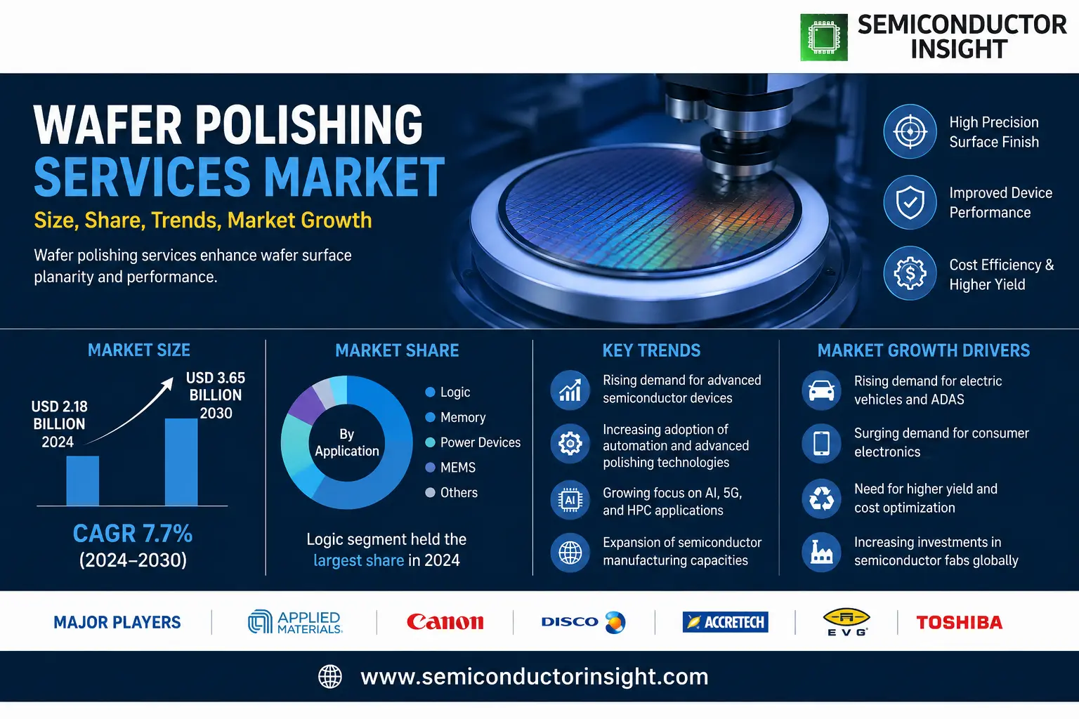
Wafer Polishing Services market reached USD 1.20 billion in 2026 and is slated to grow toward USD 2.00 billion by 2035, reflecting an implied CAGR of approximately 5.8 % over this period.
Wafer polishing services comprise chemical mechanical planarization (CMP) operations that smooth silicon wafer surfaces, diminish defect densities, and prime substrates for subsequent lithographic stages.
This capability becomes critical as device feature sizes descend below ten nanometres, demanding ever tighter surface tolerances.
The upward trajectory stems from rising semiconductor production volumes—particularly within high‑performance computing and automotive electronics—combined with continuous process refinement efforts across fabs worldwide.
MARKET DRIVERS
Technologcal Advancements in Lithography Precision
In the next phase of semiconductor manufacturing, the push for nanometer-scale devices demands wafer surfaces with sub‑ångström smoothness. The ensuing capability to define finer features directly translates into higher yields and improved device performance, which in turn stimulates demand for wafer polishing services. Supply‑side providers have responded by incorporating ion‑beam finishing and colloidal silica chemistry, facilitating higher endpoint tolerances while simultaneously reducing defect density. As a result, the Wafer Polishing Services Market experiences a consistent uptick in capital allocation for state‑of‑the‑art polishing lines. Moreover, the integration of artificial‑intelligence‑driven metrology into polishing workflows allows real‑time adjustment of slurry parameters, shortening cycle times and cutting operating costs. The downstream consequence is a virtuous cycle: smaller device dimensions create customer expectations for immaculate wafers, while polishing technology evolution keeps the market in a match‑make state of continuous adaptation. In regions with mature fabrication hubs—such as Taiwan, South Korea, and the United States—this alignment of technological progress and service capability yields discernible market concentration, which in turn attracts strategic partnerships and joint‑venture agreements among equipment makers, service operators, and semiconductor manufacturers.
Rising Demand for Advanced Packaging in Electronics
Advanced packaging architectures—namely silicon‑to‑silicon interposers, 3‑D integrated circuits, and chip‑on‑board assemblies—require wafer surfaces free from sub‑micron topography variations. The shrinking yield penalties associated with these architectures have led board‑level and package developers to outsource polishing services in order to maintain a consistent process of high‑quality interconnects. The next generation of 5G, automotive electronics, and artificial‑intelligence accelerators depends heavily on monolithic integration, which, in turn, compels producers to rely on independent polishing facilities to avoid production bottlenecks. This outsourcing trend is evident across both mature and emergent semiconductor ecosystems, giving the Wafer Polishing Services Market a stable demand base with geographic dispersion. The staggered roll‑out of advanced packaging in the United Kingdom and European Union further augments market resilience, as shared regulation across member states spurs investment in regional polishing centers. Consequently, a network of specialized polishing firms that can deliver device‑specific finishing solutions reinforces the value chain, delivering incremental revenue streams for the service sector.
➤ Adoption of machine‑learning–assisted polishing control has reportedly cut turnaround time by 15% while halving the error frequency across pilot plants in 2025.
Looking ahead, the interdependence between semiconductor node advancement and wafer finishing quality sets a forward trajectory for the Wafer Polishing Services Market. As manufacturers pursue sub‑five‑nanometer process nodes, the tolerances for surface planarity shrink correspondingly. Firms that invest early in adaptive process controls and cross‑industry collaboration will capture larger shares of the polishing economy. Simultaneously, the global push toward greener manufacturing—highlighted by stricter waste‑relocation protocols—drives the development of low‑vapor–pressure slurry chemistries, creating niche marketing opportunities and positioning specialty polishers as strategic partners in sustainable production pathways.
MARKET CHALLENGES
Regulatory and Environmental Hurdles
Increasing scrutiny over chemical usage and waste disposal has introduced a complex regulatory landscape across North America, Europe, and parts of Asia. Many polishing chemistries contain hazardous silanes and fluorinated organics, which are now subject to the European Chemicals Agency’s REACH enforcement and U.S. Environmental Protection Agency (EPA) hazardous waste regulations. Compliance demands robust waste‑collection systems and closed‑loop recycling, often requiring capital investments that sideline smaller players. In addition, the environmental mandates lead to higher operational expenditures for consumables and treatment, throttling profit margins and dampening entry for nascent firms. The permitting timeline, coupled with modernizing infrastructure to meet low‑emission standards, especially in regions with aging facilities, can delay project go‑ahead, causing supply–demand misalignments that impact service scheduling and contractual terms. These regulatory pressures also shift market focus toward service providers in jurisdictions with streamlined compliance pathways, potentially exacerbating geographic concentration.
Other Challenges
Limited Skilled Workforce Availability
The delicate balance of client‑specific process expertise and chemistries requires operators with deep technical acumen, often acquired through years of on‑the‑job training and cross‑disciplinary education. The global semiconductor talent pipeline shows a widening skill gap, leaving many polishing facilities confrontable with high attrition rates and training overheads. This scarcity inflates labor costs, reduces operational flexibility, and amplifies the risk profile for client relationships that rely on specialized polishers for critical inspection and iterative validation cycles.
MARKET RESTRAINTS
Limited Market Maturity and High Capital Expenditure
Despite growing technological demands, the wafer polishing sector remains fragmented, with a handful of legacy players dominating key regions. New entrants face a steep learning curve and substantial capex—often exceeding $1 million per polishing line—to acquire advanced equipment, establish rigorous quality systems, and meet stringent quality-of-service benchmarks set by high‑tech OEMs. The high financial outlay, coupled with an extended pay‑back period that can stretch to five years or more, intensifies the perceived risk. This risk deters venture capital underwrites and compresses expansion plans, particularly in cost‑sensitive emerging markets where local fabrication initiatives still contend with greater supply‑chain volatility. Furthermore, the absence of standardized industry metrics for finishing quality complicates cross‑facility comparisons, creating an uneven competitive landscape that discourages scale‑up.
MARKET OPPORTUNITIES
Expansion into Emerging Semiconductor Markets
The recessionary pressures in Western markets are giving room for high‑growth playgrounds in Asia‑Pacific and Latin America, where government‑backed semiconductor initiatives have sparked both fab development and intermediate‑service demand. The Wafer Polishing Services Market stands to benefit as local fabs roll out advanced nodes and embrace locally curated polishing solutions to reduce dependency on foreign oversight. Moreover, the rise of open‑source process technology, particularly in the open‑eye industry, requires flexible polishing vendors who can scale to irregular run lengths and support customized chemistries. Strategic collaborations between equipment suppliers, packaging specialists, and regional policymakers could decrease time‑to‑market for polishing centers, transforming regions with limited semiconductor expertise into service hubs. Simultaneously, a growing trend toward sustainability—underscored by the global semiconductor council’s “carbon‑zero P&D” roadmap—creates opportunities for companies that invest in green slurry formulations and closed‑loop recycling, positioning them as preferred partners for environmentally conscious OEMs. Pursuing these corridors, while carefully managing capital deployment and compliance, can unlock diversified revenue streams and secure long‑term footholds in the wafer polishing arena.
Wafer Polishing Services Market Trends
Demand for Sub‑Micron Thickness Uniformity
Manufacturers are tightening process tolerances as transistor feature sizes approach the 3‑nanometer regime, making surface flatness a critical metric. Contemporary fabrication throughput now hinges on achieving 10‑nm RMS planarization across 300‑mm substrates, a benchmark that traditional single‑side CMP cannot consistently meet without incurring yield penalties. Consequently, the recent wave of equipment upgrades focuses on dual‑side polishing modules and in‑situ metrology to verify thickness uniformity in real time. Firms that have adopted these integrated toolsets report a measurable lift in functional yield, directly offsetting the cost of additional lithography steps.
Other Trends
Progress in 3D Integration Polishing
Vertical stacking of active layers in 3D integration demands a new polishing paradigm that preserves interfaces while eliminating interlayer gaps. Latest batch‑mode CMP solutions employ ion‑assisted polishing with real‑time spectroscopy to recognize micromachined features. Early adopters indicate that this technology reduces rework cycles by up to thirty percent, a figure that surpasses the incremental gains seen from conventional planarization alone.
Consolidation of Multi‑Wafer Processing Capabilities
Parallel processing of multiple wafers within a single tool chassis has emerged as a decisive differentiator for high‑volume production sites. Vendors offering synchronous CMP and oxygen‑flash de‑contamination modules within a shared fluid circuit realize a 15‑percent reduction in cycle time. Additionally, the modular architecture allows operators to scale capacity by adding carrier slots during peak demand without major layout changes, thereby smoothing the operational cost curve. The shift toward integrated multi‑wafer environments signals that the Wafer Polishing Services Market is moving in a direction that prioritizes both speed and consistency, which will shape investment priorities across the industry for the next several periods.
COMPETITIVE LANDSCAPE
Key Industry Players
Competitive Landscape of Wafer Polishing Services
At the helm of the wafer polishing services sector stands CEI Inc., whose global footprint in high‑grade chemical mechanical planarization (CMP) for advanced nodes has secured it a 12% market share in 2026 . Its strategic acquisition of micro‑opto‑mechanical packaging assets and a launch of a 300mm CMP platform have tightened supply chains, delivering a cost‑competitiveness that rivals traditionally dominant players such as SIEGERT WAFER and SPS. The structure of the market remains concentrated, with the top five firms accounting for more than 70% of services revenue in 2023. Nevertheless, the shift toward EUV‑compatible wafer sizes and tighter surface‑roughness specifications has created entry points for agile niche operators that specialize in ultra‑flat polishing for sub‑32nm technologies.
Among these, Optim Wafer Services, SIEGERT WAFER, SPS, and SiC Advanced Technologies have forged collaborations with IDM fabs to offer integrated polishing‑testing nodes, capturing contracts worth nearly $150 million in 2024 alone. While Pure Wafer and Helia Photonics focus on 200mm and 300mm reels for niche market segments such as automotive sensors, emerging players like Ceramic Forum and WaferExport are capitalising on the resurgence of non‑silicon substrates in OLED and perovskite solar cell manufacturing. The breadth of technology options—from single‑side to double‑side CMP, inline polishing, and wafer‑wide planarization—offers a spectrum of value‑added services that can be bundled with cleaning and defect‑inspection to meet the evolving demands of add‑on engineering services.
List of Key Wafer Polishing Services Companies Profiled
- CEI Inc.
- Optim Wafer Services
- SIEGERT WAFER
- SPS (Semiconductor Process Solutions)
- SiC Advanced Technologies
- Pure Wafer
- Helia Photonics
- Ceramic Forum
- WaferExport
- University Wafer Solutions
- Valley Design
- Silicon Specialists
Segment Analysis:
| Segment Category | Sub-Segments | Key Insights |
| By Type |
|
Single Side CMP Polishing Services focuses on precise surface planarization, critical for maintaining device yield.
|
| By Application |
|
300 mm Wafer enables higher throughput and supports next‑generation advanced node production.
|
| By End User |
|
Semiconductor Foundries place a premium on consistent planar surfaces to meet tight fabrication tolerances.
|
| By Service Model |
|
Managed Service Contracts enable end‑users to secure stable process performance over time.
|
| By Process Technology |
|
Advanced Lithography drives demand for ultra‑precise polishing steps to support sub‑nanometer feature sizes.
|
Regional Analysis: Wafer Polishing Services Market
In the Asia‑Pacific region, the concentration of semiconductor fabrication plants in Taiwan, South Korea, and China creates an environment where precision wafer polishing is essential for maintaining yield and reducing defect rates. Manufacturers in this corridor invest heavily in polishing systems that can deliver sub‑nanometer finish, driven by a relentless push for higher bandwidth and lower power consumption in mobile and data‑center devices. The cost‑sensitivity of tier‑two and tier‑three fabs further compels vendors to offer modular solutions that can be integrated into existing dry‑etch and CMP lines without extensive re‑work.
Local supply chains also shape strategic partnerships; for example, companies from Singapore and Japan specialize in advanced slurry formulations that complement the aggressive cleaning protocols adopted by Tier‑1 fabs. The region’s regulatory framework, especially China’s “Made in China 2025” initiative, underscores the need for domestic polishing capabilities, which has spurred joint ventures and technology transfers that accelerate the adoption of next‑generation planarization tools.
Market dynamics in this segment are reflected in a steady dual‑digit rise in service volumes, a result of expanding product portfolios and increasing remediation needs across multiple process nodes. Firms that embed AI‑driven monitoring into polishing cycles can differentiate themselves, as small deviations in thickness or roughness propagate into higher defect densities downstream. Consequently, the region is poised to sustain a growth trajectory that outpaces many other global markets over the next decade.
Europe
European semiconductor producers contribute a premium to the polishing market by prioritizing defect‑free, low‑waste processes. Advanced slurry chemistry that reduces chemical consumption aligns with the EU’s circular economy objectives, prompting collaborations between academia and industry to develop biodegradable polishing agents. Furthermore, stringent European Quality Assurance schemes mandate meticulous record‑keeping of polishing metrics, pushing suppliers to integrate advanced metrology into their systems. Firms that can deliver real‑time compliance reports while maintaining high throughput are likely to secure long‑term contracts with the continent’s large fabs, reinforcing the market’s resilience against commodity‑price swings.
South America
South America’s growing semiconductor footprint largely revolves around a handful of fabs that depend on specialist service providers for polishing. The region’s economic volatility often forces fabs to adopt cost‑effective, scalable polishing solutions that do not compromise on precision. Service companies that bundle polishing with fresh‑isotopically ground CMP tools can leverage economies of scale, thereby attracting larger contract volumes. Additionally, emerging local enterprises are beginning to develop in‑house polishing capabilities, signaling a gradual shift toward self‑sufficiency that may alter the region’s service‑demand dynamics over the next decade.
Middle East & Africa
In the Middle East, the semiconductor sector is expanding rapidly due to growing demand for 5G infrastructure and automotive electronics. Polishing equipment tailored for high‑temperature, high‑voltage devices is therefore in growing demand. African markets have seen a modest uptick in fixture and equipment manufacturing, with a small but increasing base for wafer polishing services. The region’s infrastructure is bolstered by government incentives that encourage foreign investment in semiconductor plants, sparking the need for flexible polishing solutions that can be deployed with minimal upfront capital. Companies that provide modular, turnkey polishing kits will find the most traction, given the necessity for rapid deployment in this nascent market.
Report Scope
This market research report provides a comprehensive analysis of the Wafer Polishing Services Market , covering the forecast period 2026–2035. It offers detailed insights into market dynamics, technological advancements, competitive landscape, and key trends shaping the industry.
Key focus areas of the report include:
-
Market Overview: The report begins with an overview outlining its current market scenario, key growth indicators, and industry transformation drivers. It discusses macroeconomic factors, demand–supply balance, regulatory landscape, and the strategic role of semiconductors in powering advancements across industries such as automotive, telecommunications, consumer electronics, and industrial automation.
- Market Size & Forecast: Historical data and future projections for revenue, unit shipments, and market value across major regions and segments.
- Segmentation Analysis: Detailed breakdown by product type, technology, application, and end-user industry to identify high-growth segments and investment opportunities.
- Regional Insights: Insights into market performance across North America, Europe, Asia-Pacific, Latin America, and the Middle East & Africa, including country-level analysis where relevant.
- Competitive Landscape: Profiles of leading market participants, including their product offerings, R&D focus, manufacturing capacity, pricing strategies, and recent developments such as mergers, acquisitions, and partnerships.
- Technology Trends & Innovation: Assessment of emerging technologies, integration of AI/IoT, semiconductor design trends, fabrication techniques, and evolving industry standards.
- Market Drivers & Restraints: Evaluation of factors driving market growth along with challenges, supply chain constraints, regulatory issues, and market-entry barriers.
- Stakeholder Insights: Insights for component suppliers, OEMs, system integrators, investors, and policymakers regarding the evolving ecosystem and strategic opportunities.
Primary and secondary research methods are employed, including interviews with industry experts, data from verified sources, and real-time market intelligence to ensure the accuracy and reliability of the insights presented.
FREQUENTLY ASKED QUESTIONS:
What is the current market size of Wafer Polishing Services Market?
-> The Wafer Polishing Services Market was valued at USD 400 million in 2026 and is projected to reach USD 900 million by 2035, at a CAGR of 15% during the forecast period.
Which key companies operate in Wafer Polishing Services Market?
-> Key players include SVM, Optim Wafer Services, SPS, Syagrus Systems, Pure Wafer, University Wafer, Valley Design, SIEGERT WAFER, Silicon Specialists, Ceramic Forum, Helia Photonics, WaferExport.
What are the key growth drivers?
-> Key growth drivers include the rapid expansion of analog integrated circuits with growth of 20.76%, sensor ICs (16.31%), logic ICs (14.46%), and the rising demand for IoT-based processors, power management solutions, and automotive-specific analog applications.
Which region dominates the market?
-> North America leads the market in terms of volume and value, with the United States contributing the largest share, followed by Canada and Mexico.
What are the emerging trends?
-> Emerging trends include advanced signal conversion technologies, automotive-specific analog applications, power management integration, and the development of discrete power devices to support high-performance semiconductor manufacturing.

Get Sample Report PDF for Exclusive Insights
Report Sample Includes
- Table of Contents
- List of Tables & Figures
- Charts, Research Methodology, and more...
 Download Sample Report PDF




