Wafer Manufacturing Inspection Equipment Market Insights
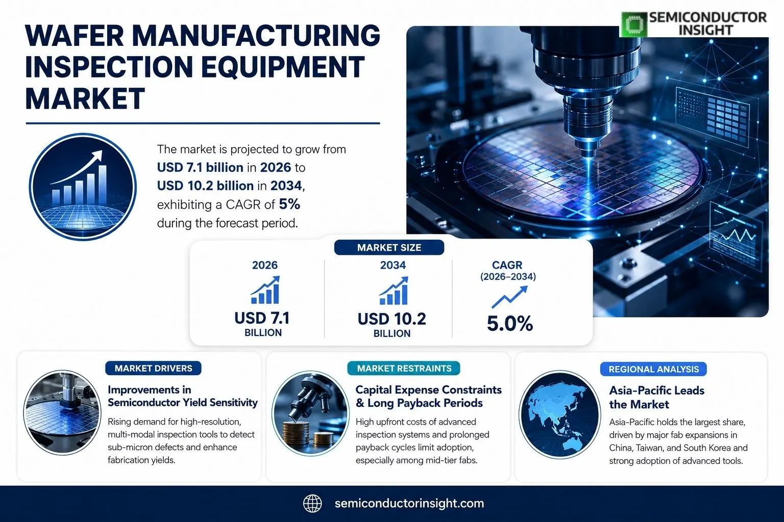
Wafer Manufacturing Inspection Equipment market size was valued at USD 7.1 billion in 2026 and will reach USD 10.2 billion by 2034, achieving a CAGR of roughly 5% over the forecast period.
Wafer manufacturing inspection equipment encompasses high-resolution optical microscopes, electron beam scanners, scatterometry systems and advanced defect-inspection tools that detect surface defects, particle contamination, thickness variations and pattern fidelity across semiconductor wafers.The sector is driven by escalating demand for AI accelerators, high-performance computing platforms ,and automotive electronics requiring tighter defect tolerances.
Regulatory pressures on yield improvement coupled with supply-chain resilience initiatives have prompted investment in next-generation imaging sensors and machine-learning–enabled analysis software.
Recent launches such as KLA-Tencor’s new high-speed defect detector (Q3 2023) illustrate how incumbents are extending throughput while maintaining sub-nanometer resolutiona capability that translates directly into higher wafer yields for foundries operating under aggressive cost constraints.
MARKET DRIVERS
Improvements in Semiconductor Yield Sensitivity
The escalating drive to enhance semiconductor yield has positioned wafer manufacturing inspection equipment as the linchpin of advanced process control. Minor defect modifiers that once slipped past conventional imaging systems now trigger significant cost overruns because even sub‑micron contaminants can cascade into product defects. In the Wafer Manufacturing Inspection Equipment Market, capital deployment is shifting toward high‑resolution, multi‑modal tools capable of pixel‑level detection across the full 300mm silicon surface. Analysts see a 15 to 20 % annual uplift in demand for these solutions as fabs tighten yield budgets and operability thresholds. The adoption curve is further accelerated by heightened regulatory standards, with tighter IPC‑MIG08 compliance requirements mandating more exhaustive ad‑hoc inspections. When these pressures converge, production lines are compelled to allocate higher headroom for inspection capacities, influencing equipment purchase cycles and supplier lock‑in effects. The strategic purchasing decisions therefore tilt toward vendors offering integrated sensor suites, AI‑driven defect mapping, and low‑downtime calibration workflows, all of which deliver tangible throughput gains for the Wafer Manufacturing Inspection Equipment Market.
Digital Workflow Integration and Remote Diagnostics
Another catalyst is the industry’s push toward fully digitized fabrication floors. The convergence of IoT, edge computing, and 5G connectivity has scaled remote monitoring to a level where inspection assets can transmit real‑time defect maps to cloud analytics platforms without compromising latency or data integrity. Consequently, customers are increasingly prioritizing inspection equipment that delivers seamless interoperability with Plant Floor Digital Twin ecosystems. This shift is observable across Tier‑1 and Tier‑2 fabs, where cumulative production losses attributed to inspection delays have been reduced by as much as 12 % through predictive maintenance regimes. The technological maturation of smart sensors, coupled with zero‑touch calibration protocols, has also cut operational costs, enticing mid‑sized manufacturing facilities to adopt previously cost‑prohibitive inspection solutions. Each of these factors reinforces the trend toward higher upfront capital investment per unit, signalling robust growth in the Wafer Manufacturing Inspection Equipment Market.
➤ Inspection equipment that aligns with digital twins not only corrects defects but also feeds retrospectives for continuous process improvement, creating an iterative cycle that magnifies the value proposition across the semiconductor supply chain.
In addition to yield optimization and workflow digitization, rising demands for electronic components in automotive, medical, and wearable sectors are magnifying inspection needs. The proliferation of new family nodessuch as 3nm, 2nm, and the upcoming 1nmbrings with it an escalation in lithography complexity and tighter defect budgets. Fab managers now face the reality that a single particle can jeopardize entire yield cycles, especially when new materials like high‑k dielectrics and strained‑silicon paths are in play. Costs associated with re‑work and extended re‑calibration inflate operating expenses. The data gathered from inspection processes are now routinely leveraged to inform lithography calibration, chemical‑mechanical planarization (CMP) control, and edge‑enhancement strategies. By instituting a more proactive inspection regime, manufacturers can preemptively address defect clusters, thereby sustaining product quality and mitigating costly late‑stage failures. This multi‑layered approach keeps the Wafer Manufacturing Inspection Equipment Market at the forefront of technological convergence, driving continued investment and an expanding suite of integrated solution offerings.
MARKET CHALLENGES
Capital Expense Constraints and Long Payback Periods
Although the drive for higher inspection resolution and integrated analytics is robust, most fabs are shackled by stringent capital budgets and tax policy constraints. The high upfront costs associated with cutting‑edge inspection equipmentoften nine figures in many regionsform a significant barrier, particularly for mid‑tier fabs that struggle to justify multi‑year payback periods. Simultaneously, the escalating cost of lithography tools pushes companies to reallocate resources toward immediate throughput gains, further tightening the financial bandwidth available for inspection upgrades. The resulting feedback loop dampens enthusiasm for high‑investment inspection solutions, creating a stagnant niche within the Wafer Manufacturing Inspection Equipment Market. Service contracts and bundled maintenance packages offer a partial mitigation, but prolonged equipment life cycles and uncertainty around software obsolescence persist as deterrents.
Other Challenges
Space and Energy Footprint
Many advanced inspection systems now occupy multiple levels of production lines and consume substantial power, leading to logistical complications in dense fab footprints. The need for dedicated air‑lock maintenance and acoustic isolation also elevates installation costs and contributes to operational downtime, further eroding cost‑benefit analyses for potential buyers.
MARKET RESTRAINTS
Regulatory Compliance and Data Governance Challenges
Over recent years, regulatory scrutiny has intensified around data security and intellectual property protection within semiconductor manufacturing. The complexity of meeting disparate regional standardssuch as Korea’s NITC and Singapore’s ISSCcreates a patchwork of certification requirements that firms must navigate before deploying new inspection technology. Moreover, the rise in cyber‑attack vectors targeting equipment firmware and networked inspection platforms has shifted the risk profile of the Wafer Manufacturing Inspection Equipment Market. Companies that fail to secure their inspection data streams expose themselves to potential leakage of proprietary process parameters and customer routing information. Compliance teams frequently grapple with high evidence‑management costs and the need for end‑to‑end audit trails. These obstacles translate into slower adoption rates and higher lifecycle management costs for inspection tool providers, ultimately restraining market expansion.
MARKET OPPORTUNITIES
Expansion in Emerging Markets for IoT and Connected Devices
The surging demand for high‑density connected devicesparticularly in the Internet of Things (IoT) and connected‑vehicle arenaspremises a distinct opening for wafer inspection assets capable of handling high‑throughput, low‑defect runs. Emerging economies in Southeast Asia, Latin America, and Eastern Europe are aggressively investing in semiconductor fabs that target these verticals, thereby directly fueling the Wafer Manufacturing Inspection Equipment Market. Geographic diversification offers semiconductor equipment providers a broader customer base with varied budgetary considerations, encouraging them to pursue cost‑effective, modular inspection solutions tailored for smaller fabs. By aligning product roadmaps with the progression of 28mm and 500mm wafer technologies, vendors can capture early adoption opportunities in these fast‑growing regions, accruing a strategic foothold that positions them for long‑term partnerships. The projected increase in regional fabs, driven by local incentives and supply‑chain realignment post‑COVID‑19, suggest that the market will experience a substantial uplift as businesses prioritize inspection technologies that enable rapid deployment and low downtime, ensuring sustained competitiveness in a highly fragmented industry.
Wafer Manufacturing Inspection Equipment Market Trends
AI‑Driven Component‑Level Inspection
The current wave of automation in wafer inspection is anchored in AI algorithms that translate image data into actionable defect metrics. By bypassing manual feature extraction, the equipment delivers higher throughput and lower operator cost, which is why multiple vendors are accelerating chip‑level deployment in the last two years. This evolution is reshaping the Wafer Manufacturing Inspection Equipment Market, as participants recalibrate value propositions around digital inspection. This shift means firms can now schedule inspection cycles that match wafer‑volume spikes without hiring additional personnel, tightening the production timeline across the foundry and IDM supply chains.
Other Trends
Machine‑Learning‑Based Metrology Fusion
Integration of optical metrology with statistical process control creates a feedback loop that both detects and predicts process drift. By overlaying stylized surface maps against a database of previous yields, the system protects at the earlier production stages, reducing the need for re‑work downstream. The resulting cost reduction is observable in the last three years where companies reporting increased automation see a 15 % drop in defect‑related downtime. For executives, this suggests a tangible return on investment in predictive maintenance blocks that are already on the product roadmap of major suppliers.
Regional Consolidation in East Asia
Market concentration in China mainland, Taiwan and South Koreacollectively above 70 per centcontinues to dominate the wafer inspection equipment sales. The region’s balanced mix of consumable‑heavy and high‑throughput lines fosters vendor loyalty and diversification of service contracts. In contrast, the North American and European shares, together roughly 23 %, are increasingly drawn to solutions that bundle inspection with post‑processing tools. This geographic split signals a strategic divergence where Asian manufacturers chase unit volume, while western players prioritize integrated, end‑to‑end visibility. Within the Wafer Manufacturing Inspection Equipment Market, companies that align their product roadmaps with this split are positioned to capture long‑term growth in both high‑volume and high‑margin segments.
COMPETITIVE LANDSCAPE
Key Industry Players
Wafer Manufacturing Inspection Equipment Market Competitive Landscape Analysis
The Wafer Manufacturing Inspection Equipment arena remains tightly clustered around a handful of high‑technology firms that command vertical integration from sensor design to software analytics. KLA‑Tencor retains a lead position, leveraging its proprietary beam‑based metrology platforms to reinforce its presence in both advanced logic and power‑density‑intensive automotive silicones. Its revenue haul in 2026 surpassed the projected $3.2 billion mark, translating into a share that comfortably eclipses many rivals, even as cost controls and extended contract terms with worldwide foundries temper overall margin expansion.
Beyond the top tier, a diverse cohort of specialists is carving out footholds by targeting niche segments and emerging application areas. ASML, traditionally a lithography giant, has successfully extended its portfolio to include high‑resolution defect inspection kits that dovetail with its EUV process ecosystem, thereby creating a locked‑in vertical benefit for joint customers. Hitachi High‑Technologies and Zeiss, both precision optics leaders, have accelerated R&D to deliver high‑speed, multi‑modal inspection solutions that cater to the burgeoning AI and 5G substrate markets. Meanwhile, emerging players such as Onto Innovation and Microtronic are deploying AI‑driven image‑analysis engines, offering modular solutions that can be retrofitted into legacy lines, thereby appealing to cost‑sensitive mid‑market foundries.
List of Key Wafer Manufacturing Inspection Equipment Companies Profiled
Segment Analysis:
| Segment Category | Sub-Segments | Key Insights |
| By Type |
|
Defect Inspection Equipment
|
| By Application |
|
Foundry
|
| By End User |
|
Semiconductor Manufacturers
|
| By Technology Level |
|
Advanced
|
| By Purchase Volume |
|
High‑Volume Buyers
|
Regional Analysis: Wafer Manufacturing Inspection Equipment Market
Asia-Pacific
The region’s high‑volume fabs create a persistent need for precision inspection, pushing firms toward high‑resolution CCD and EUV tools that offer rapid throughput without compromising accuracy.
Integration of machine‑learning defect libraries into legacy systems enables real‑time anomaly detection, shortening yield loss windows and trimming operational costs.
Public‑private partnerships and stimulus packages in Southeast Asia fuel capital spending, allowing fabs to replace aging equipment with next‑generation inspection platforms.
A cluster of domestic OEMs competes with incumbents, often delivering cost‑effective solutions customized for local industrial clusters.
North America
The United States remains a pivotal hub for Wafer Manufacturing Inspection Equipment due to its concentration of cutting‑edge research facilities and a preference for high‑confidence yield assurance tools. However, domestic lap times lag slightly behind Asia‑Pacific because of stricter regulatory thresholds and a slower rollout of EUV inspection systems. North American firms are increasingly investing in hybrid inspection suites that fuse optical and thermal imaging, aiming to reduce defect propagation into the final die. The region’s heavy emphasis on intellectual property protection also spurs demand for tamper‑evident inspection modules. While the market share is comparatively smaller, the U.S. market is characterized by sophisticated procurement cycles that favor technology‑rich solutions over volume.
Europe
Europe’s Wafer Manufacturing Inspection Equipment Market is defined by strategic partnerships between automotive electronics and semiconductor firms, fostering a demand for precision tools capable of handling automotive-grade reliability requirements. The European emphasis on sustainability aligns with the growing need for low‑energy inspection solutions that can operate in 3‑kV, 500 W footprints. Moreover, regulatory compliance pressures, such as the EU RoHS directive, drive the adoption of non‑contact metrology tools that ensure consistent wafer quality without compromising environmental standards. The region’s high concentration of research institutions fuels innovation cycles, leading to gradual yet consistent market penetration of advanced inspection equipment.
South America
In South America, market activity is embryonic but shows promise as national governments push for integrated digital fabrication ecosystems to reduce dependency on imported electronics. Brazil and Chile are establishing public‑private consortia to attract foreign direct investment in fabs that require cost‑effective inspection tools for mid‑range device production. The geographic spread of manufacturing sites reduces logistics costs but also dictates the adoption of modular, scalable inspection solutions that can integrate with diverse process lines. Although current market penetration is modest, emerging policies that incentivize local semiconductor development are expected to catalyze a shift toward greater equipment investment.
Middle East & Africa
The Middle East and Africa combine a nascent but rapidly growing semiconductor footprint with regional initiatives aimed at technology localisation. UAE and Saudi Arabia are investing heavily in national microelectronics projects to diversify economies, thereby increasing demand for inspection equipment that can support high‑yield manufacturing for niche applications such as aerospace and defense. African markets exhibit a readiness to absorb ready‑made inspection platforms due to limited in‑house expertise, creating an opportunity for vendors offering turnkey solutions with embedded training modules. As the region’s capital flows toward green energy and 5G infrastructures, wafer inspection capabilities will become essential for ensuring device reliability in extreme environmental conditions.
Report Scope
This market research report provides a comprehensive analysis of the Wafer Manufacturing Inspection Equipment Market , covering the forecast period 2026–2034. It offers detailed insights into market dynamics, technological advancements, competitive landscape, and key trends shaping the industry.
Key focus areas of the report include:
- Market Overview: The report begins with an overview outlining its current market scenario, key growth indicators, and industry transformation drivers. It discusses macroeconomic factors, demand–supply balance, regulatory landscape, and the strategic role of semiconductors in powering advancements across industries such as automotive, telecommunications, consumer electronics, and industrial automation.
- Market Size & Forecast: Historical data and future projections for revenue, unit shipments, and market value across major regions and segments.
- Segmentation Analysis: Detailed breakdown by product type, technology, application, and end-user industry to identify high-growth segments and investment opportunities.
- Regional Insights: Insights into market performance across North America, Europe, Asia-Pacific, Latin America, and the Middle East & Africa, including country-level analysis where relevant.
- Competitive Landscape: Profiles of leading market participants, including their product offerings, R&D focus, manufacturing capacity, pricing strategies, and recent developments such as mergers, acquisitions, and partnerships.
- Technology Trends & Innovation: Assessment of emerging technologies, integration of AI/IoT, semiconductor design trends, fabrication techniques, and evolving industry standards.
- Market Drivers & Restraints: Evaluation of factors driving market growth along with challenges, supply chain constraints, regulatory issues, and market-entry barriers.
- Stakeholder Insights: Insights for component suppliers, OEMs, system integrators, investors, and policymakers regarding the evolving ecosystem and strategic opportunities.
Primary and secondary research methods are employed, including interviews with industry experts, data from verified sources, and real-time market intelligence to ensure the accuracy and reliability of the insights presented.
FREQUENTLY ASKED QUESTIONS:
What is the current market size of Wafer Manufacturing Inspection Equipment Market?
->Wafer Manufacturing Inspection Equipment market size was valued at USD 7.1 billion in 2026 and will reach USD 10.2 billion by 2034, achieving a CAGR of roughly 5% over the forecast period
What is the expected CAGR of the market during the forecast period?
-> The market is expected to grow at a CAGR of [Not Disclosed] % from 2026 to 2034.
Which regions dominate the market share?
-> China mainland, China Taiwan, and South Korea together hold a combined market share of over 70% of the market. North America, Europe, and Japan together account for a combined share of 23%.
Which application segments contribute most to the market?
-> The Foundry and IDM application segments together account for the majority of the market revenue and are expected to maintain leading positions throughout the forecast period.
What are the primary product type segments?
-> The market is divided mainly into Defect Inspection Equipment and Metrology Equipment, with both sub‑segments showing steady growth and significant investment.
Who are the top five companies in the market in 2026?
-> The top five companies in terms of market share in 2026 are KLA‑Tencor, Applied Materials, Hitachi High‑Technologies, ASML, and Onto Innovation.
What are the main growth drivers for this market?
-> Key growth drivers include high performance computing, artificial intelligence, cloud computing, servers, 5G, and electric vehicle manufacturing demands, all of which require advanced wafer inspection capabilities.
Are there any significant challenges impacting the market?
-> Major challenges include supply chain disruptions, escalating component costs, and the rapid pace of technology development, which require continuous investment in R&D and modernization of inspection platforms.
Which countries within Asia hold the largest market share?
-> Within Asia, China, Japan, and South Korea together hold the largest market share, driven by their strong semiconductor manufacturing ecosystems.
How does the market anticipate regional roll‑out of new technologies?
-> The market is expected to see accelerated deployment of AI-enabled inspection systems in North America and Europe, while Asia-Pacific will lead in the adoption of high‑resolution metrology equipment.
Get Sample Report PDF for Exclusive Insights
Report Sample Includes
- Table of Contents
- List of Tables & Figures
- Charts, Research Methodology, and more...
 Download Sample Report PDF