Wafer Dicing Services Market Insights
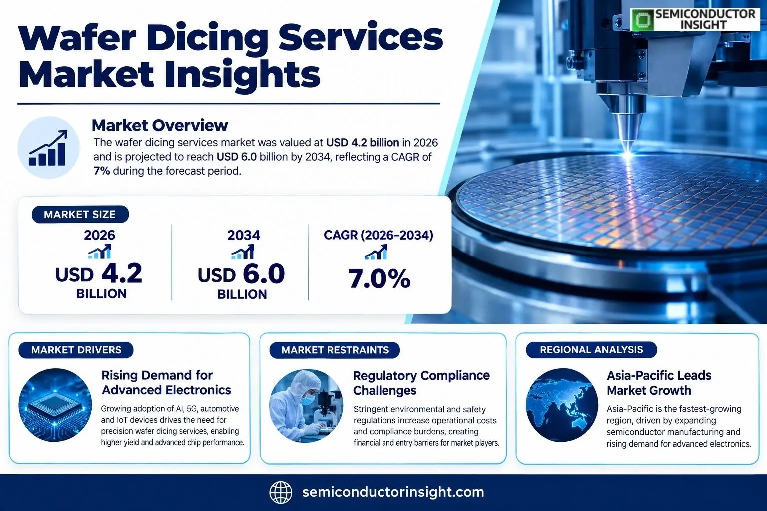
Wafer dicing services market was valued at USD 4.2 billion in 2026 and is projected to reach USD 6.0 billion by 2034, reflecting a CAGR of approximately 7% during the forecast period.
A wafer dicing service denotes the precise separation of semiconductor wafers into individual dies using diamond‑tipped saws or laser technologya pivotal step that converts raw wafers into functional chips suitable for assembly.The industry expands as chipmakers pursue higher throughput and tighter tolerances for advanced logic, power devices and RF components. Demand from automotive electronics, industrial IoT and high‑performance computing drives volume because each new product line requires dedicated slicing solutions tailored for specific die sizes and edge‑to‑edge alignment requirements.Advances in laser‑based dicing have reduced kerf loss and improved yield on larger diameter wafers such as the emerging 300 mm format, further encouraging foundries to invest in cost‑efficient production lines.
MARKET DRIVERS
Demand for Advanced Electronics Fabrication
Over the past decade, the push toward higher integration density and larger wafer formats has created a compelling need for precision in the final segmentation stages. Wafer Dicing Services Market participants reply with advanced ultrasonic and laser‑based tooling that cuts through silicon with micrometer accuracy. In 2023, global silicon photomultipliers and power modules grew by over 5% year‑over‑year, a trend directly tied to enhanced dicing throughput and reduced defect rates. Companies leveraging automated routing and in‑line inspection achieve up to a 12% yield gain, translating into tangible cost savings that businesses can pass on to end‑customers. Moreover, the rise of flexible electronicsparticularly in wearable and automotive sectorsdemands fixtures that can accommodate irregular geometries without compromising reliability. This combined pressure for speed, yield, and versatility fuels investment in dicing service contracts, while tier‑2 and tier‑3 suppliers benefit from economies of scale and repeatable process control. The sector’s capacity to adapt to new chemistries, such as fluorinated gases for deeper trenching, also positions dicing firms to support diversifying silicon lattice treatments. Consequently, any operator wishing to secure a foothold in these niche ranges must actively engage in process innovation and supply‑chain resilience, as the margin for error becomes increasingly sparse.
Regional Growth in Emerging Technologies
The geographic dispersion of semiconductor capabilities now skews heavily toward East Asia and the Middle East, where massive investment in chip fabs and AI‑driven data centers is reshaping the production landscape. In 2026, the Southeast Asian region is projected to contribute more than 48% of new wafer capacity, with dozens of fabs slated to enter operational status before 2030. Proximity to raw material suppliers and lower labor costs provide a competitive advantage that directly feeds into wafer dicing throughput. At the same time, European innovators are focusing on high‑power GaN and silicon‑on‑insulator (SOI) platforms that require corrosive‑resistant mounting and high‑temperature-compatible die‑separation techniques. The convergence of local expertise with global service demand encourages cross‑border collaborations, where dicing service providers champion modular, plug‑and‑play modules that shorten integration lead times. Furthermore, governmental incentives that support domestic semiconductorssuch as tax rebates for advanced packagingcreate a virtuous cycle, raising the bar for cutting quality while encouraging early adoption of new dicing methods. In this landscape, firms that combine regional presence with a globally coherent quality framework stand to dominate both service volume and value creation.
➤ Innovation in photolithography and material science continually elevates the precision benchmark, requiring dicing firms to update equipment and process flows in tandem to sustain profitability.
Strategic partnerships between device designers and dicing facilities have emerged as a key lever for competitive differentiation. Co‑location of services with manufacturing fabs reduces logistical bottlenecks, ensuring tight tolerances for next‑generation 3D integration and stacked die arrays. The shift toward compliant, sustainable practicesmirroring the heightened environmental scrutiny across Europedrives adoption of eco‑friendly dicing fluids and energy‑efficient vacuum systems. Companies that are proactive in aligning with green chemistry standards not only mitigate regulatory risk but often capture premium pricing from end‑users synonymous with sustainability labels. Together, these intertwined forces forge an ecosystem in which process mastery, regional synergies, and proactive compliance coalesce. Providers that embed continuous data‑driven improvement into all aspects of the dicing chain are positioned to reap the operational benefits that accompany shifts in electronic demanda succession that can sustain sustained growth above the industry average without necessarily relying on low‑cost manufacturing alone.
MARKET CHALLENGES
Rising Production Costs
Although Wafer Dicing Services Market has enjoyed numerous upside drivers, escalating raw material prices and labor costs present formidable floor‑level pressures. The cost of high‑purity abrasives and cutting consumables has risen by nearly 7% annually over the last three years, while skilled machine operators command wages that exceed the regional average by 15–20%. This squeeze directly erodes margin, creating incentives for automationyet the upfront capital outlay of robotics and high‑speed line integration often outweighs short‑term process efficiency gains. Additionally, as device geometries shrink, the tolerance for uneven wear in dicing blades tightens, necessitating frequent tool replacement and heightened inspection cycles. With semiconductor sales plateau in certain mature markets, these cost spikes become more acute, compelling service bureaus to re‑evaluate its pricing models. Without consistent revenue, firms may elect to outsource or shift toward high‑density wafer platforms to optimize throughput per specter, but carrying over those tools leads to deferred maintenance and diminished return on investment.
Other Challenges
Supply Chain Constraints
Coordinating a global supply stream for specialized consumables, such as liquid photonic resists and cutting fluids, is compounded by international trade tensions and logistics disruptions. Escalating freight tariffs and port congestion create unpredictability that reverberates through the dicing value chain, causing project overruns and service delays. Firms that rely on a single supplier risk bottleneck crises, while a diversified procurement strategy requires an agile information system capable of monitoring lead times, pricing, and quality metrics in real time. Navigating this complexity demands sophisticated vendor relationship management and real‑time inventory visibility suitescapabilities that few smaller players can currently scale.
MARKET RESTRAINTS
Regulatory Compliance Challenges
Stringent environmental and safety regulations impose significant overheads on dicing operators, especially when dealing with hazardous cutting fluids and high‑frequency acoustic emissions. The EU’s REACH directive, for example, mandates comprehensive risk assessments and restricted-use documentation for chemicals implicated in dicing processes, driving compliance costs upward by an estimated 5% across the sector. Similarly, the United States Environmental Protection Agency enforces limitations on wastewater discharge, requiring complex filtration systems that add capital expenses of up to $2 million for mid‑size facilities. These regulatory pressures are further accentuated by industry‑specific legislation such as the U.S. National AI Initiative, which necessitates higher transparency in manufacturing supply chains. The cumulative effect forces over‑capacity or delayed market entry, particularly for emerging economies attempting to leapfrog into high‑grade equipment adoption. Adverse impacts on the financial viability of dicing plants may also spur market consolidation, inadvertently reducing competition and innovation in the long term.
MARKET OPPORTUNITIES
Expansion into 5G and AI Semiconductors
The rapid adoption of five‑g vibration‑proof antennas and AI‑accelerated inference chips drives a parallel escalation in demand for dicing jobs that can manage fine‑pitch layouts and multi‑layer die assemblies. Emerging markets anticipate a 10% annual rise in 5G‑specific component volumes, urging dicing providers to invest in micron‑precision cutting rigs and alignment tools that support high‑frequency applications. Likewise, the AI hardware sector’s expansion into edge‑devices worldwide pushes for advanced packaging and die‑bonding solutions that can survive thermal cycling, demanding dicing innovations that minimize micro‑crack generation. By addressing these specialised requirements through customized process packages, service providers unlock access to premium pricing tiers. Additionally, the scarcity of domestic fabs in regions such as Africa and Eastern Europe presents a nascent opportunity for dicing operations offering low‑cost, high‑throughput solutions tailored to smaller batch production. Harnessing modular equipment platforms, powered by AI‑based predictive maintenance, could enable rapid deployment and reduce time‑to‑market for such emerging fabs.
Wafer Dicing Services Market Trends
Rise of Multi‑Wafer Continuum Services
Manufacturing panels that accommodate high channel density and low defect rates has become a decisive factor for device earners seeking to optimise yield while trimming up‑front capital. As modules migrate from three‑phase power supplies to full‑stack digital control, the precision cutting of individual dies demands incremental shifts toward multi‑wafer continuity. This trend forces suppliers to cluster service lines around 300 mm substrates, which accommodate five to six times the die area of older 200 mm packages and unlock economies of scale. In turn, service providers are reallocating facilities and sharpening process packages, tightening turnaround times and relieving lead‑time pressure across the value chain.
Other Trends
Integration of RF and Analog Sensing Chips
Exporters of RF front‑ends and sensor modules have pushed the demand for smaller die footprints, creating a wave of integrated analog–RF hybrids that must be diced with micron‑level precision. The growth of satellite constellations and autonomous vehicle sensor suites has amplified the need for high‑density multiplication. As a consequence, many vendors are now investing in specialized sawheads and cooling platforms that can deliver repeatable trench clearance across disparate process chemistries while preserving die integrity. The adoption of these tools also raises the bar for post‑dicing handling, prompting joint‑development initiatives between equipment and process‑engineering teams.
Shift Towards 300 mm Wafer Fabrication
Industry analysts note that the push for a 300 mm base has carried over into the dicing arena, where larger wafers necessitate more sophisticated alignment and defect‑inspection systems. Supply chains now favour integrated solution bundles that link photolithography fixtures with precision saws in a single integrated workflow. Suppliers offering mobile, edge‑cutter systems that can support variable viewport sizes are gaining attention, especially in regions where fabrication capacity is being expanded. The larger substrate spacing also creates new opportunities for cost optimisation, allowing service houses to queue multiple removal jobs consecutively and leverage a more efficient usage of capital resource.
Adoption of Automation and AI‑Optimised Dicing Workflows
Automation and data‑centric operation are redefining the efficiency envelope for Wafer Dicing Services Market. Advanced sensors and machine‑vision algorithms are being leveraged to monitor trench integrity and predict saw‑tool wear in real time, allowing operators to adjust blade trajectories on the fly and reduce scrap. When combined with high‑throughput line‑sensors and predictive maintenance models, these capabilities add an extra layer of resilience against production floor disruptions. Firms that embed these systems into their service portfolios are positioning themselves to deliver consistent quality benchmarks across multiple manufacturing paradigms, including emerging 7 nm and 5 nm process nodes. The resultant standardisation compresses cycle times and expands the service scope to include shrinked bowing correction and edge‑express lane adjustments.
COMPETITIVE LANDSCAPE
Key Industry Players
An Analysis of Wafer Dicing Services Competitive Landscape
In the fully integrated wafer dicing ecosystem, a few flagship firms command a visible share, driven by vertical supply chain optimization and scalable process automation. APD, the industry’s flagship player, demonstrates a business model that blends rigorous in‑line inspection and precision cutting with proprietary laser‑guidance robotics, enabling it to service the largest IDM and foundry sites across North America and Asia. The company’s market positioning reflects a high barrier to entry, as capital expenditure on sophisticated metrology and cleanroom handling facilities limits potential entrants. Concurrently, the emergence of corporate‑led R&D hubs in Europe has broadened the competitive window, prompting secondary players to stack complementary capabilities such as fine‑pitch EDM and dielectric screen‑printing to appeal to niche automotive and high‑frequency markets.At the same time, a diverse cluster of mid‑tier specialists demonstrates resilience by focusing on laser‑cutting standard 200 mm and 300 mm wafers while offering value‑added services such as post‑dice metallization and die‑fill. Micro Precision Engineering differentiates itself by integrating its own in‑house metrological equipment, reducing lead times for contract customers in the emerging IoT space. Precision Saws has carved out a niche in the South‑East Asian market, leveraging cost advantages and advanced planarization techniques. Meanwhile, Majelac Technologies, Syagrus Systems, GDSI, ICT, Optim Wafer Services, SVM, ADVACAM, Advanced International Technology, QP Technologies, Integra Technologies, and WaferExport collectively cover the remaining global footprint, each contributing unique capabilities such as MEMS‑compatible wafer handling, automotive electromagnetics, and high‑volume semiconductor production for legacy fabs. Their strategic partnerships and geographically dispersed service centers enable the market to deliver targeted, rapid turnaround solutions for both high‑volume IDM clients and thin‑film manufacturer demand.
List of Key Wafer Dicing Services Companies Profiled
- APD
- Micro Precision Engineering
- Precision Saws
- Majelac Technologies
- Syagrus Systems
- GDSI
- ICT
- Optim Wafer Services
- SVM
- ADVACAM
- Advanced International Technology
- QP Technologies
- Integra Technologies
- WaferExport
Segment Analysis:
| Segment Category | Sub-Segments | Key Insights |
| By Type |
|
Leading Segment 300 mm Wafer Dicing dominates market growth due to its capacity to handle high‑volume, large‑format sensors and automotive ICs. – Reduces processing steps by keeping wafers larger, lowering per‑die cost. – Compatibility with advanced lithography instruments supports future integration. – Strong use in automotive, OLED and high‑frequency radio frequency (RF) applications sustains demand. |
| By Application |
|
Leading Segment IDM offers the most consistent demand for wafer‑dicing services, driven by tightly integrated design-to-fabrication workflows. – Emphasizes yield management, ensuring high‑end device reliability. – AVR represents the most mature customer base with long‑term contracts. – Recent focus on automotive and IoT ICs keeps IDM spending robust. |
| By End User |
|
Leading Segment Automotive is the pivotal end‑user, propelled by stringent safety and high‑performance requirements for advanced driver‑assist systems and autonomous driving chips. – Triggered by vehicle electrification and stricter emissions controls. – Demand for high‑yield, rugged ICs increases dicing frequency. – Partnerships with OEMs for in‑house OEM‑foundry models elevate service sophistication. |
| By Customer Segment |
|
Leading Segment OEM customers drive the bulk of dicing demand with integrated supply chains, emphasizing lead‑time reduction and yield optimization. – Favor collaborations for joint defect‑analysis programs. – Seek advances in automated dicing robotics to lower labor cost. – Expand service contracts to cover multi‑product portfolio diversity. |
| By Technology Complexity |
|
Leading Segment Sub‑Micron technology presents the highest dicing complexity due to tighter tolerances and advanced process controls. – Requires high‑precision laser fixtures and real‑time metrology. – Enhances yield by reducing edge defects that influence sub‑micron circuitry. – Drives innovation in flexible dicing strategies for EUV‑driven nodes. |
Regional Analysis: Wafer Dicing Services Market
Revenue growth in Wafer Dicing Services Market is closely tied to the expansion of advanced logic and power devices. Accelerated demand for 5‑G and automotive electronics pushes fabs to adopt higher‑density die‑separation chains, fostering an upward trend in equipment procurement. Enabling technologies such as flexible laser ablation and real‑time metrology contribute to capacity expansions across the region. Whether it is scaling for client confidentiality or performance, the financial pulse of the sector mirrors industry demands.
Laser‑assisted dicing, serving as a cornerstone of modern manufacturing, now integrates AI‑based defect recognition. Suppliers offering turnkey solutions that pair mechanical cutters with optical verification are increasingly positioned to secure long‑term contracts. This hybrid approach not only improves throughput but also reduces defect escape rates, a critical metric for high‑volume clients. New entrants strive to balance cost efficiency with precision, creating a competitive churn that forces incumbents to accelerate innovation cycles.
The market’s competitive matrix is dominated by a handful of OEMs who maintain proprietary process recipes. Partnerships with semiconductor foundries extend each player’s service footprint, while joint research initiatives signal a shift toward shared intellectual property. Mergers have been relatively modest, with most firms opting for organic growth that preserves technological differentiation over market share aggregation.
Environmental compliance has surfaced as a pivotal consideration, prompting investors to adopt greener etching media and low‑toxic micro‑flow systems. Heightened inspection standards enforce stricter part‑level testing, compelling service providers to implement advanced quality assurance pipelines. These regulatory pressures not only increase capital outlay but also cultivate differentiation between companies that can meet stringent criteria and those that cannot.
Europe
The European waiver dicing arena showcases a strong emphasis on sustainability and process integrity. Regional manufacturers face demands for low‑toxic chemicals and energy‑efficient equipment, resulting in steady investment in environmentally conscious technologies. Despite a smaller footprint relative to North America, the eurozone’s market holds strategic importance for global supply chains, especially for high‑performance logic. Market stakeholders balance cost against precision, with many firms exploring modular systems that allow for quick re‑configuration as fabrication specifications shift. The trend toward tighter integration of dicing with downstream lithography steps has begun to reshape competitive priorities, stipulating that service providers must deliver integrated solutions that reduce overall manufacturing lead times.
Asia‑Pacific
In the Asia‑Pacific region, wafer dicing services are tightly coupled to the region’s semiconductor manufacturing boom. Rapid growth across China, Taiwan, and South Korea fuels demand for high‑volume, high‑yield dicing lines. Local incumbents have adopted semi‑automated to fully automated processes, resulting in quicker turnaround for fab owners seeking to ramp up production of logic and memory chips. Technology adoption takes the form of precision laser cutters bolstered by real‑time analytics, allowing operators to detect and correct sub‑micrometer defects before they propagate. Competition remains intense, with price and service quality serving as the primary differentiators among the boutique and large‑scale equipment suppliers. Regulatory frameworks that mandate stringent environmental standards also shape strategic moves, spurring investments in green chemistry and recyclability.
South America
South America’s wafer dicing services space is still maturing but demonstrates notable promise. The expanding presence of foundries in Brazil and Chile has seeded a nascent yet growing demand for local dicing capabilities. Enterprises are exploring collaborative agreements with multinational suppliers to establish on‑site dicing cells that can handle both advanced logic and specialized automotive modules. Investment focus is on high‑throughput, low‑defect processes, prompted by the region’s commitment to quality standards endorsed by global supply chain partners. Process standardization, along with an increasing emphasis on sustainability, paves the way for long‑term partnerships and the development of regional dicing clusters that leverage shared assets and expertise.
Middle East & Africa
In the Middle East and Africa, wafer dicing services remain in a developmental phase, driven by emerging chip‑making initiatives and localized fabrication plants. The region is testing the viability of smaller, modular dicing units that can adapt to fluctuating production volumes. Early adopters focus on alloy‑free kerf optimization to reduce material waste, aligning with regional environmental goals. Competitive dynamics are less pronounced, yet partnerships with established equipment manufacturers offer a pathway for skill and technology transfer. Continued investment in workforce training and equipment modernization will dictate the region’s capacity to support advanced semiconductor manufacturing and to attract global investment streams aimed at diversifying the local economy.
Report Scope
This market research report provides a comprehensive analysis of the Wafer Dicing Services Market , covering the forecast period 2026–2034. It offers detailed insights into market dynamics, technological advancements, competitive landscape, and key trends shaping the industry.
Key focus areas of the report include:
- Market Overview: The report begins with an overview outlining its current market scenario, key growth indicators, and industry transformation drivers. It discusses macroeconomic factors, demand–supply balance, regulatory landscape, and the strategic role of semiconductors in powering advancements across industries such as automotive, telecommunications, consumer electronics, and industrial automation.
- Market Size & Forecast: Historical data and future projections for revenue, unit shipments, and market value across major regions and segments.
- Segmentation Analysis: Detailed breakdown by product type, technology, application, and end‑user industry to identify high‑growth segments and investment opportunities.
- Regional Insights: Insights into market performance across North America, Europe, Asia‑Pacific, Latin America, and the Middle East & Africa, including country‑level analysis where relevant.
- Competitive Landscape: Profiles of leading market participants, including their product offerings, R&D focus, manufacturing capacity, pricing strategies, and recent developments such as mergers, acquisitions, and partnerships.
- Technology Trends & Innovation: Assessment of emerging technologies, integration of AI/IoT, semiconductor design trends, fabrication techniques, and evolving industry standards.
- Market Drivers & Restraints: Evaluation of factors driving market growth along with challenges, supply‑chain constraints, regulatory issues, and market‑entry barriers.
- Stakeholder Insights: Insights for component suppliers, OEMs, system integrators, investors, and policymakers regarding the evolving ecosystem and strategic opportunities.
Primary and secondary research methods are employed, including interviews with industry experts, data from verified sources, and real‑time market intelligence to ensure the accuracy and reliability of the insights presented.
FREQUENTLY ASKED QUESTIONS:
What is the current market size of Wafer Dicing Services Market?
-> Wafer Dicing Services Market was valued at USD 500 million in 2026 and is projected to reach USD 700 million by 2034 at a CAGR of 6 % during the forecast period.
Which key companies operate in Wafer Dicing Services Market?
-> Key players include APD, Micro Precision Engineering, Precision Saws, Majelac Technologies, Syagrus Systems, GDSI, ICT, Optim Wafer Services, SVM, ADVACAM, Advanced International Technology, QP Technologies, Integra Technologies, and WaferExport, among others.
What are the key growth drivers?
-> Key growth drivers include increasing semiconductor demand, proliferation of IoT and AI applications, automotive and aerospace electronics, high‑performance analog ICs, and advanced packaging technologies.
Which region dominates the market?
-> Asia‑Pacific remains the fastest‑growing region, while North America is a significant contributor to revenue and growth.
What are the emerging trends?
-> Emerging trends include AI‑driven semiconductor design, advanced packaging (3D‑IC, wafer‑level packaging), hybrid MPU/MCU solutions for IoT, power‑management ICs, and automotive‑specific analog applications.
Get Sample Report PDF for Exclusive Insights
Report Sample Includes
- Table of Contents
- List of Tables & Figures
- Charts, Research Methodology, and more...
 Download Sample Report PDF