
Wafer Cleaning (Single Waofr , Batch) System Market Insights
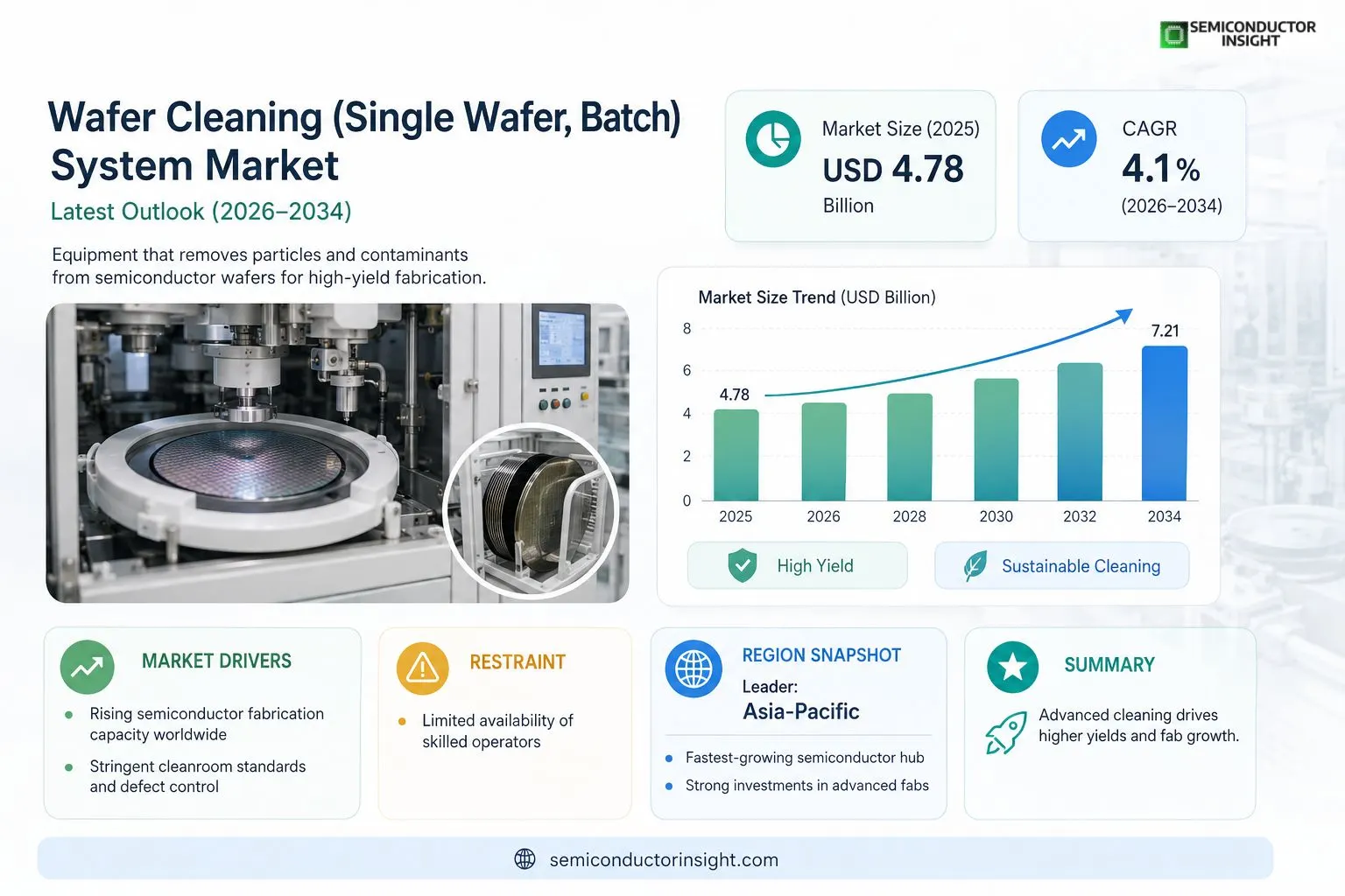
Global Wafer Cleaning (Single Wafer, Batch) System Market size was valued at USD 4.78 billion in 2025. The market is projected to grow from USD 5.02 billion in 2026 to USD 7.21 billion by 2034, exhibiting a CAGR of 4.1% during the forecast period.
Wafer cleaning systems are essential equipment used in semiconductor fabrication to eliminate particles, residues and contaminants from silicon wafers. Single‑wafer tools treat each wafer individually for precise control; batch tools process multiple wafers concurrently to boost throughput, employing chemical‑mechanical polishing, megasonic agitation and advanced rinse technologies.The market is accelerating because semiconductor demand surges,driven by advanced nodes and AI chips,prompting fabs to adopt more efficient cleaning solutions. While rising material costs present challenges, continued R&D investments and collaborations,such as the 2023 partnership between Tokyo Electron and Entegris on megasonic cleaning,are expected to propel adoption across leading manufacturers.
MARKET DRIVERS
Increasing Semiconductor Fabrication Capacity
Wafer Cleaning (Single Wafer, Batch) System Market is being propelled by a rapid expansion of fab lines worldwide, especially in regions investing heavily in 5‑nm and sub‑5‑nm technologies. Higher wafer throughput requirements drive manufacturers to adopt cleaning solutions that deliver consistent defect reduction while maintaining cycle times under 30 seconds per wafer.
Stringent Cleanroom Standards
Global cleanroom classifications such as ISO 14644‑1 Class 1 and Class 10‑level specifications force fabs to implement advanced cleaning chemistries and low‑particle‑generation equipment. This regulatory pressure translates into greater investment in single‑wafer and batch cleaning platforms that can meet tighter particle limits without compromising yield.
➤ “Adoption of plasma‑based single‑wafer cleaners is projected to rise by double‑digits annually as fabs target sub‑10 nm node yields.”
Coupled with the need for environmentally friendly solvents and water‑recycling capabilities, these drivers create a compelling value proposition for equipment vendors seeking to differentiate in a competitive landscape.
MARKET CHALLENGES
High Capital Expenditure
Deploying state‑of‑the‑art cleaning systems often requires multi‑million‑dollar outlays for tooling, automation integration, and facility upgrades, making cost a critical barrier for smaller or emerging fabs.
Other Challenges
Technology Integration
Legacy process equipment may lack the communication interfaces needed for seamless data exchange with modern cleaning solutions, necessitating additional engineering effort and extending implementation timelines.
MARKET RESTRAINTS
Limited Availability of Skilled Operators
Operating sophisticated single‑wafer cleaning tools requires specialized training. A shortage of qualified technicians can slow adoption rates, as fabs allocate resources to build internal expertise.Furthermore, the complexity of process optimization,balancing chemical concentration, plasma power, and dwell time,adds operational overhead that many manufacturers find challenging to manage efficiently.Finally, regulatory compliance for hazardous chemicals used in certain batch cleaning processes can delay projects, especially in regions with stringent environmental legislation.
MARKET OPPORTUNITIES
Emerging AI‑Driven Process Control
Artificial intelligence and machine‑learning algorithms are being integrated into cleaning equipment to provide real‑time defect monitoring and adaptive recipe adjustments, promising higher yields and reduced waste.In addition, the growing demand for silicon carbide (SiC) and gallium nitride (GaN) wafers opens a niche for customized cleaning solutions capable of handling these harder materials without surface damage.Finally, sustainable solvent‑free cleaning technologies, such as nanodispersion‑based methods, present a green‑innovation pathway that aligns with the industry’s increasing focus on carbon‑neutral manufacturing.
Wafer Cleaning (Single Wafer, Batch) System Market Trends
Shift Toward Single‑Wafer Precision for Advanced Nodes
The semiconductor industry is increasingly targeting sub‑10 nm nodes, where defect density directly influences yield. In response, fabs are prioritizing single‑wafer cleaning tools because they deliver tight process control and enable real‑time monitoring of particle removal. This precision approach reduces variability and aligns with the push for AI‑centric chips, where even minimal contamination can affect performance. The adoption rate of single‑wafer systems has accelerated over the past two years, driven by equipment manufacturers offering modular interfaces that integrate seamlessly with existing lithography lines.
Other Trends
Batch Processing Efficiency Gains
While single‑wafer solutions dominate high‑mix environments, batch cleaning remains essential for high‑volume production. Recent upgrades in megasonic agitation and advanced rinse chemistry have lifted throughput by up to 20 % without compromising particle‑level cleanliness. Operators report lower chemical consumption per wafer, which mitigates rising material costs. The blend of batch capacity and improved energy efficiency is prompting several large foundries to expand their batch lines while preserving a parallel single‑wafer capability for critical process steps.
Integration of Megasonic and Chemical‑Mechanical Technologies
Collaborations between equipment vendors and specialty material suppliers have produced hybrid cleaning modules that combine megasonic acoustic fields with chemical‑mechanical polishing (CMP) fluids. These integrated platforms can switch between gentle particle removal and aggressive surface planarization within a single cycle, shortening overall wafer handling time. Field data indicate a reduction of cycle time by roughly 15 seconds per wafer, which aggregates to significant fab floor space savings over a full production shift. As Wafer Cleaning (Single Wafer, Batch) System Market continues to evolve, the convergence of acoustic and chemical techniques is expected to set a new baseline for both yield improvement and operational cost control.
COMPETITIVE LANDSCAPEKey Industry Players
Wafer Cleaning (Single Wafer, Batch) System Market Competitive Landscape
Wafer Cleaning Market is dominated by a handful of large equipment manufacturers that leverage deep semiconductor process expertise and extensive global service networks. Tokyo Electron (TEL) leads the single‑wafer segment with its advanced megasonic and chemical‑mechanical cleaning platforms, capitalizing on strong fab contracts in Asia and the United States. Lam Research and Applied Materials follow closely, offering batch‑type systems that integrate high‑throughput rinse and drying modules, enabling fabs to meet the rising throughput demands of AI‑driven chip production. SCREEN Semiconductor Solutions complements the landscape with niche niche wafer‑scrubbing technologies that address specialty processes, while Entegris supplies critical consumables and megasonic cleaning kits that are often bundled with OEM equipment. This concentration of capabilities creates a tiered market structure where a few tier‑1 vendors command the majority of revenue, supported by a broad ecosystem of mid‑size and specialist firms.Beyond the tier‑1 giants, several niche players contribute significant innovation and market depth. KLA Corporation focuses on defect inspection‑linked cleaning solutions that enhance yield for leading‑edge nodes. Hitachi High‑Technologies provides precision ultrasonic cleaning tools tailored for advanced packaging applications. MKS Instruments supplies process control hardware that improves cleaning cycle stability. PVA TePla (Germany) and SPTS Technologies (UK) offer specialized batch cleaning equipment for emerging markets, while companies such as Advanced Semiconductor Engineering (ASE) and Ultratech (an Advantest company) extend their service portfolios with customized cleaning modules for fab‑level integration. This diverse set of providers ensures competitive pricing, rapid technology refresh cycles, and localized support for semiconductor manufacturers worldwide.
List of Key Wafer Cleaning Companies Profiled
- Tokyo Electron Ltd.
- Lam Research Corporation
- Applied Materials, Inc.
- SCREEN Semiconductor Solutions Co., Ltd.
- Entegris, Inc.
- KLA Corporation
- Hitachi High‑Technologies Corporation
- MKS Instruments, Inc.
- PVA TePla GmbH
- SPTS Technologies Ltd.
- Advanced Semiconductor Engineering (ASE)
- Ultratech (Advantest)
Segment Analysis:
| Segment Category | Sub-Segments | Key Insights |
| By Type |
|
Single‑Wafer Cleaning
|
| By Application |
|
Front‑End Process Cleaning
|
| By End User |
|
Foundries
|
| By Process Stage |
|
Post‑CMP Cleaning
|
| By Technology Trend |
|
Megasonic Cleaning
|
Regional Analysis: North America
United States
The market is witnessing continuous innovation in cleaning technologies, including plasma cleaning, chemical cleaning, and ultrasonic cleaning. These advancements are aimed at improving cleaning efficiency, reducing chemical consumption, and minimizing environmental impact.
Stringent environmental regulations regarding chemical usage and waste disposal are significantly influencing the development and adoption of more sustainable cleaning solutions. Compliance with these regulations is a key consideration for market participants.
The Wafer Cleaning System Market in the US is competitive, with key players focusing on product differentiation, technological leadership, and strategic partnerships to gain market share. Consolidation and mergers & acquisitions are also observed in the industry.
The adoption of AI and machine learning for process optimization and predictive maintenance is emerging as a key trend, improving cleaning system performance and reducing downtime.
Europe
Europe exhibits a strong and technologically advanced semiconductor industry, driving demand for sophisticated Wafer Cleaning (Single Wafer, Batch) System Market. The region’s focus on high-performance computing, automotive electronics, and IoT devices fuels the need for precise and reliable cleaning solutions. Stringent environmental regulations, particularly within the EU, are promoting the adoption of eco-friendly cleaning chemistries and processes. Several key players in the industry have a significant presence in Europe, offering a wide range of cleaning systems tailored to specific customer requirements. The emphasis on energy efficiency and sustainable manufacturing practices is influencing the development of next-generation cleaning technologies. Research and development initiatives supported by European funding bodies are further contributing to innovation in this sector. The market is characterized by a highly skilled workforce and a strong emphasis on quality and reliability.
Asia-Pacific
Asia-Pacific is the largest and fastest-growing market for Wafer Cleaning (Single Wafer, Batch) System Market globally. Driven by the rapid expansion of semiconductor manufacturing in countries like China, Taiwan, and South Korea, the region presents significant growth opportunities. The increasing demand for consumer electronics, 5G infrastructure, and electric vehicles is fueling the need for advanced wafer cleaning solutions. The market is characterized by a mix of domestic and international players, with a strong focus on cost-effectiveness and localized service support. Government initiatives supporting the development of domestic semiconductor industries are further accelerating market growth. The Asia-Pacific region is also witnessing a shift towards higher-end cleaning systems to meet the demands of advanced node manufacturing. However, concerns around supply chain disruptions and geopolitical tensions pose potential challenges to the market’s sustained growth.
South America
South America represents a relatively smaller but growing market for Wafer Cleaning (Single Wafer, Batch) System Market. The expansion of the electronics industry in countries like Brazil and Argentina is driving demand for wafer cleaning solutions. The region’s focus on automotive electronics, telecommunications, and industrial automation is contributing to market growth. While the market is currently dominated by imports, there is increasing interest in local manufacturing capabilities. The adoption of advanced cleaning technologies is progressing, driven by the need to meet the stringent requirements of semiconductor manufacturers.
Middle East & Africa
The Middle East & Africa region is an emerging market for Wafer Cleaning (Single Wafer, Batch) System Market with significant growth potential. The expansion of the electronics industry in countries like Saudi Arabia, the UAE, and South Africa is driving demand for wafer cleaning solutions. Government initiatives to diversify economies and invest in technology are further supporting market growth. The region’s focus on telecommunications, aerospace, and defense is contributing to the need for advanced cleaning systems. The market is relatively new, with opportunities for both established players and new entrants.
Report Scope
This market research report provides a comprehensive analysis of the Wafer Cleaning (Single Wafer, Batch) System Market , covering the forecast period 2026–2034. It offers detailed insights into market dynamics, technological advancements, competitive landscape, and key trends shaping the industry.
Key focus areas of the report include:
- Market Overview: The report begins with an overview outlining its current market scenario, key growth indicators, and industry transformation drivers. It discusses macroeconomic factors, demand–supply balance, regulatory landscape, and the strategic role of semiconductors in powering advancements across industries such as automotive, telecommunications, consumer electronics, and industrial automation.
- Market Size & Forecast: Historical data and future projections for revenue, unit shipments, and market value across major regions and segments.
- Segmentation Analysis: Detailed breakdown by product type, technology, application, and end-user industry to identify high-growth segments and investment opportunities.
- Regional Insights: Insights into market performance across North America, Europe, Asia-Pacific, Latin America, and the Middle East & Africa, including country-level analysis where relevant.
- Competitive Landscape: Profiles of leading market participants, including their product offerings, R&D focus, manufacturing capacity, pricing strategies, and recent developments such as mergers, acquisitions, and partnerships.
- Technology Trends & Innovation: Assessment of emerging technologies, integration of AI/IoT, semiconductor design trends, fabrication techniques, and evolving industry standards.
- Market Drivers & Restraints: Evaluation of factors driving market growth along with challenges, supply chain constraints, regulatory issues, and market-entry barriers.
- Stakeholder Insights: Insights for component suppliers, OEMs, system integrators, investors, and policymakers regarding the evolving ecosystem and strategic opportunities.
Primary and secondary research methods are employed, including interviews with industry experts, data from verified sources, and real-time market intelligence to ensure the accuracy and reliability of the insights presented.
FREQUENTLY ASKED QUESTIONS:
What is the current market size of Wafer Cleaning (Single Wafer, Batch) System Market?
-> Wafer Cleaning (Single Wafer, Batch) System Market was valued at USD 4.78 billion in 2025 and is expected to reach USD 7.21 billion by 2034. The forecast period exhibits a CAGR of 4.1%.
Which key companies operate in Wafer Cleaning (Single Wafer, Batch) System Market?
-> Key players include major semiconductor equipment manufacturers such as Tokyo Electron, Entegris, Lam Research, Applied Materials, and Hitachi High‑Technologies.
What are the key growth drivers?
-> Growth is driven by the accelerating demand for semiconductors, especially advanced nodes and AI chips, which push fabs to adopt more efficient wafer cleaning solutions.
Which region dominates the market?
-> The market is global with no single region explicitly identified as dominant; growth is observed across major semiconductor manufacturing hubs worldwide.
What are the emerging trends?
-> Emerging trends include the adoption of megasonic cleaning technologies and strategic collaborations such as the 2023 partnership between Tokyo Electron and Entegris.

Get Sample Report PDF for Exclusive Insights
Report Sample Includes
- Table of Contents
- List of Tables & Figures
- Charts, Research Methodology, and more...
 Download Sample Report PDF


