
Wafer Carriers for MOCVD Market Insights
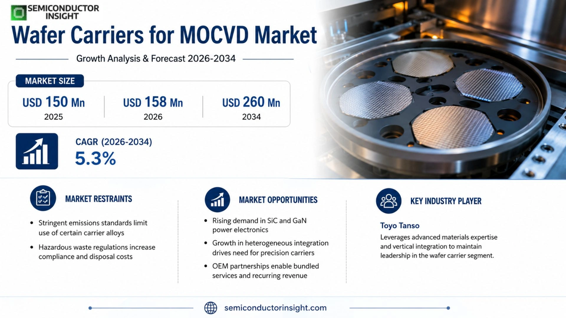
Wafer Carriers for MOCVD market size was valued at USD 150 million in 2025. The market is projected to grow from USD 158 million in 2026 to USD 260 million by 2034, exhibiting a CAGR of 5.3% during the forecast period.
Epitaxy susceptor,commonly referred to as a wafer carrier for metal‑organic chemical vapor deposition (MOCVD),is a precision‑engineered holder that supports semiconductor wafers while epitaxial layers are deposited. By providing uniform thermal distribution and minimizing particle contamination, these carriers enable consistent crystal growth essential for high‑performance GaN, InP and other compound‑semiconductor devices.
The upward trajectory is anchored in the expanding demand for compound semiconductors across LED lighting, advanced packaging and high‑frequency communications. Recent activity includes Toyo Tanso’s launch of a high‑temperature carbon‑based susceptor line in March 2024 and SGL Carbon’s partnership with a leading LED manufacturer to co‑develop low‑thermal‑expansion carriers. Such initiatives underscore the sector’s focus on reliability and throughput as manufacturers scale production of next‑generation optoelectronic components.
MARKET DRIVERS
Increasing Demand for Advanced Semiconductor Devices
The rise of 5G infrastructure, AI acceleration chips, and autonomous‑vehicle sensors has intensified the need for higher‑performance epitaxial layers. Manufacturers turn to Wafer Carriers for MOCVD Market solutions that can sustain tighter temperature gradients and reduce defect propagation, thereby delivering yields that meet the aggressive cost targets of these high‑volume programs.
Cost‑Efficiency Pressures in Production
Foundries are compressing cycle times to stay competitive. Modern carrier designs featuring low‑mass alloys and optimized slot geometry enable quicker loading and unloading, cutting downtime by up to 12 %. This operational advantage translates directly into lower per‑wafer processing expense, a factor that executives cite as a decisive lever for capital allocation.
➤ “Adopting next‑generation carriers has trimmed our fab’s throughput loss by nearly a day each month, a tangible win in a margin‑squeezed market.”
Beyond immediate throughput gains, robust carrier performance also reduces the frequency of re‑work, protecting the supply chain from ripple effects that can otherwise amplify inventory costs. The compounded savings reinforce the strategic importance of carrier innovation within Wafer Carriers for MOCVD Market.
MARKET CHALLENGES
Complexities in Carrier Material Compatibility
Different epitaxial chemistries (e.g., GaN, InP, SiC) demand carriers that can withstand distinct corrosive environments. Selecting a mismatch can accelerate carrier degradation, leading to particle contamination and wafer breakage. Companies therefore must maintain a diversified material portfolio, which inflates R&D spend and lengthens qualification cycles.
Other Challenges
Supply Chain Volatility
Raw‑material shortages for high‑purity quartz and specialty alloys have sporadically driven carrier lead times beyond the typical 6‑week window. When a key supplier experiences a production halt, fabs are forced to reroute orders, incurring higher logistics costs and potential schedule slippage.
Moreover, the scarcity of skilled engineers capable of integrating new carrier designs into existing MOCVD lines creates a talent bottleneck. Training programs are expanding, yet the lag between curriculum rollout and on‑floor competence remains a palpable risk.
MARKET RESTRAINTS
Regulatory and Environmental Constraints
Stringent emissions standards in major semiconductor hubs limit the use of certain carrier alloys that release volatile compounds during high‑temperature operation. Facilities must either invest in additional abatement equipment or switch to alternative materials, both of which raise capital outlays.
In addition, waste‑handling regulations classify spent carriers as hazardous when they contain residual precursors. Compliance mandates traceable disposal pathways, adding an administrative layer that some smaller players find prohibitive.
The cumulative effect of these rules is a deceleration in the adoption curve for novel carrier technologies, as firms weigh the incremental compliance cost against incremental performance gains.
MARKET OPPORTUNITIES
Emerging Applications in Power Electronics
Power‑device manufacturers are scaling silicon‑carbide and gallium‑nitride production to meet the efficiency demands of data‑center converters and electric‑vehicle inverters. These substrates require carriers that can maintain ultra‑flat temperature profiles, a niche where Wafer Carriers for MOCVD Market innovators are already positioning proprietary solutions.
Another growth vector stems from the rise of heterogenous integration platforms, where multiple epitaxial layers are stacked within a single wafer. Precision‑engineered carriers that minimize wafer bowing and stress gradients enable tighter layer alignment, unlocking designs previously deemed impractical.
Finally, collaborations between equipment OEMs and carrier manufacturers are spawning integrated service packages that bundle carrier lifecycle management with predictive maintenance analytics. This bundled offering not only differentiates vendors but also creates recurring‑revenue streams that appeal to capital‑conscious fabs.
Wafer Carriers for MOCVD Market Trends
Growing Adoption of Compound Semiconductors Fuels Demand for High‑Performance Susceptors
The surge in GaN‑based power devices, InP photonic components, and emerging optoelectronic applications is reshaping requirements for epitaxial growth equipment. Wafer Carriers for MOCVD Market participants are responding by engineering susceptors that balance thermal uniformity with mechanical robustness, a combination critical to maintaining layer thickness control across 2‑inch to 6‑inch wafers. Suppliers such as Toyo Tanso and SGL Carbon have introduced low‑thermal‑expansion carbon‑composite carriers, which mitigate wafer warpage during high‑temperature processes. This technical evolution reduces scrap rates in high‑volume production lines, directly improving factory‑gate profitability for LED lighting manufacturers and advanced packaging firms.
Other Trends
Regional Shifts Toward Asia‑Pacific Production Hubs
China, South Korea, and Japan are concentrating investments in MOCVD clusters, largely because domestic fabs are scaling up GaN transistor output. The concentration of semiconductor foundries in these countries creates a localized pull for carriers that can withstand rapid thermal cycling inherent to large‑scale epitaxy. Concurrently, Southeast Asian governments are offering incentives for high‑purity carbon‑based component manufacturers, encouraging new entrants to supply the supply chain. This geographic redistribution is prompting Western players to form joint ventures that leverage regional cost structures while preserving technology transfer.
Supply Chain Resilience and Material Innovation
Recent disruptions in graphite mining have highlighted the vulnerability of traditional carrier materials. In response, several firms have accelerated research into silicon‑carbide and boron‑nitride substrates, which promise comparable thermal conductivity with superior chemical inertness. The transition to these alternatives is not merely a risk‑mitigation measure; it also opens opportunities for differentiated product lines targeting niche markets such as space‑qualified optoelectronics, where thermal stability under extreme conditions is non‑negotiable. Companies that successfully integrate these novel materials into their product portfolios are likely to capture premium pricing segments and set new performance benchmarks for Wafer Carriers for MOCVD Market.
COMPETITIVE LANDSCAPE
Key Industry Players
Competitive Overview of Wafer Carriers for MOCVD (2024‑2031)
Toyo Tanso continues to dominate the wafer‑carrier segment, leveraging its deep expertise in high‑purity silicon carbide and graphite technologies. The company’s vertically integrated supply chain,from raw material sourcing to precision machining,creates pricing leverage that smaller rivals struggle to match. SGL Carbon and Tokai Carbon occupy the second tier, each commanding a sizeable share in Europe and Japan respectively through differentiated product portfolios that address both GaN and InP epitaxy platforms. Consolidation pressure is evident, as the top three firms collectively account for roughly half of global shipments, prompting mid‑size manufacturers to pursue strategic alliances or niche specialization to sustain profitability.
Beyond the dominant trio, a diverse set of niche players injects innovation into the market. Bay Carbon and Schunk Xycarb Technology focus on custom‑shaped susceptor solutions for advanced MEMS and LED lighting applications, often collaborating directly with equipment OEMs. ZhiCheng Semiconductor and Mersen have carved out a foothold in the Chinese and European markets by offering cost‑effective yet thermally stable carriers for emerging compound‑semiconductor fabs. CoorsTek supplies ceramic‑based carriers that excel in high‑temperature processes, while Veeco Instruments and Aixtron broaden their value propositions by bundling carriers with their MOCVD toolsets. Additional entrants such as Sumitomo Electric, Norstel, and DIL Technology maintain regional relevance through specialized alloy compositions and rapid prototyping capabilities, ensuring the market remains fragmented despite the strength of the leading firms.
List of Key Wafer Carriers for MOCVD Companies Profiled
- Toyo Tanso
- SGL Carbon
- Tokai Carbon
- Mersen
- Bay Carbon
- CoorsTek
- Schunk Xycarb Technology
- ZhiCheng Semiconductor
- Veeco Instruments
- Aixtron SE
- Sumitomo Electric Industries
- Norstel
- DIL Technology
Segment Analysis:
| Segment Category | Sub-Segments | Key Insights |
| By Type |
|
GaN‑based carriers
|
| By Application |
|
LED Lighting
|
| By End User |
|
Semiconductor Fabricators
|
| By Wafer Size |
|
6‑inch carriers
|
| By Growth Technique |
|
MOCVD
|
Regional Analysis: Wafer Carriers for MOCVD Market
Asia‑Pacific
Industry leaders such as Samsung, SK Hynix, and TSMC have entrenched production lines that rely on precise wafer handling. Their procurement strategies now favor carriers that can endure repeated thermal cycles without compromising surface integrity, catalyzing a shift toward bespoke carrier chemistries tailored to each fab’s process window.
Recent disruptions highlighted the fragility of single‑source logistics. Vendors are diversifying material sources and establishing regional buffer stocks, ensuring uninterrupted flow of carrier components even amid geopolitical tensions or transport bottlenecks.
Research parks in Shenzhen and Hsinchu host collaborative programs that merge academic breakthroughs with commercial carrier designs. The rapid prototyping environment accelerates the transition from lab‑scale formulas to production‑ready carriers, shortening time‑to‑market for cutting‑edge MOCVD solutions.
Government incentives targeting semiconductor self‑sufficiency have allocated funding for carrier R&D. These subsidies lower entry barriers for emerging suppliers, expanding the competitive set and fostering price‑performance improvements across the region.
North America
In North America, Wafer Carriers for MOCVD Market evolves under the influence of major research institutions and a mature equipment ecosystem. Customers prioritize carriers that can support the stringent reliability standards of aerospace and defense applications, driving vendors to emphasize low‑contamination processes. The region’s investment in domestic chip fabrication, buoyed by recent policy initiatives, is creating a modest but steady demand for localized carrier production, encouraging strategic partnerships between U.S. OEMs and specialty material firms.
Europe
European players view carrier technology through the lens of sustainability and regulatory compliance. The emphasis on circular manufacturing has spurred interest in reusable carrier platforms that minimize waste while maintaining performance. Additionally, the EU’s focus on advanced photonics and quantum devices amplifies the need for carriers capable of handling ultra‑thin epitaxial layers, prompting niche players to develop high‑precision solutions that align with Europe’s green‑tech agenda.
South America
South America remains an emerging arena for Wafer Carriers for MOCVD Market, with Brazil and Chile leading modest fab expansions. Growth is constrained by limited capital expenditure, yet the region benefits from a cost‑advantageous labor pool that attracts niche subcontractors. These firms often act as cost‑effective suppliers for larger Asian assemblers, positioning South America as a supplemental source of carrier components rather than a primary innovation hub.
Middle East & Africa
The Middle East & Africa region is witnessing incremental interest in semiconductor manufacturing as part of broader diversification strategies. While local fabs are few, governmental initiatives in the UAE and Saudi Arabia to establish technology parks have sparked early demand for high‑quality carriers. Suppliers are capitalizing on this nascent market by offering turnkey carrier solutions bundled with technical training, laying the groundwork for future ecosystem development.
Report Scope
This market research report provides a comprehensive analysis of the Wafer Carriers for MOCVD Market , covering the forecast period 2026–2034. It offers detailed insights into market dynamics, technological advancements, competitive landscape, and key trends shaping the industry.
Key focus areas of the report include:
- Market Overview: The report begins with an overview outlining its current market scenario, key growth indicators, and industry transformation drivers. It discusses macroeconomic factors, demand–supply balance, regulatory landscape, and the strategic role of semiconductors in powering advancements across industries such as automotive, telecommunications, consumer electronics, and industrial automation.
- Market Size & Forecast: Historical data and future projections for revenue, unit shipments, and market value across major regions and segments.
- Segmentation Analysis: Detailed breakdown by product type, technology, application, and end-user industry to identify high-growth segments and investment opportunities.
- Regional Insights: Insights into market performance across North America, Europe, Asia-Pacific, Latin America, and the Middle East & Africa, including country-level analysis where relevant.
- Competitive Landscape: Profiles of leading market participants, including their product offerings, R&D focus, manufacturing capacity, pricing strategies, and recent developments such as mergers, acquisitions, and partnerships.
- Technology Trends & Innovation: Assessment of emerging technologies, integration of AI/IoT, semiconductor design trends, fabrication techniques, and evolving industry standards.
- Market Drivers & Restraints: Evaluation of factors driving market growth along with challenges, supply chain constraints, regulatory issues, and market-entry barriers.
- Stakeholder Insights: Insights for component suppliers, OEMs, system integrators, investors, and policymakers regarding the evolving ecosystem and strategic opportunities.
Primary and secondary research methods are employed, including interviews with industry experts, data from verified sources, and real-time market intelligence to ensure the accuracy and reliability of the insights presented.
FREQUENTLY ASKED QUESTIONS:
What is the current market size of Wafer Carriers for MOCVD Market?
-> Wafer Carriers for MOCVD market is projected to grow from USD 158 million in 2026 to USD 260 million by 2034, exhibiting a CAGR of 5.3%
Which key companies operate in Wafer Carriers for MOCVD Market?
-> Key players include Toyo Tanso, SGL Carbon, Tokai Carbon, Mersen, Bay Carbon, CoorsTek, Schunk Xycarb Technology, ZhiCheng Semiconductor.
What are the key growth drivers?
-> Key growth drivers include the increasing demand for compound semiconductor materials in high‑performance electronic and optoelectronic devices, continuous advancements in semiconductor technology, and expanding adoption of compound semiconductors across various applications.
Which region dominates the market?
-> Asia is the leading region, with strong contributions from China, Japan, and South Korea.
What are the emerging trends?
-> Emerging trends include development of advanced epitaxy susceptor materials for improved thermal management, integration of AI/IoT for process optimization, and the push towards more efficient compound semiconductor manufacturing.

Get Sample Report PDF for Exclusive Insights
Report Sample Includes
- Table of Contents
- List of Tables & Figures
- Charts, Research Methodology, and more...
 Download Sample Report PDF




