Silicon Carbide Wafer and Polishing Pad Market Insights
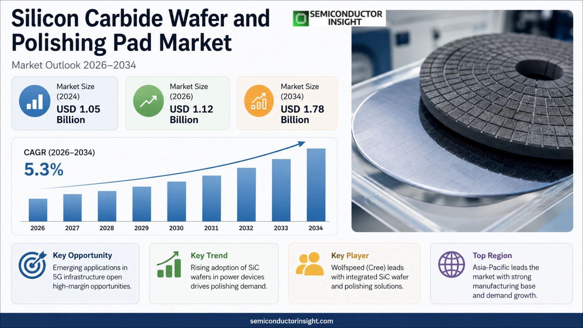
Silicon Carbide Wafer and Polishing Pad market size was valued at USD 1.05 billion in 2024. The market is projected to grow from USD 1.12 billion in 2026 to USD 1.78 billion by 2034, exhibiting a CAGR of 5.3% during the forecast period.
Silicon carbide wafers are single‑crystal substrates employed in high‑power, high‑frequency semiconductor devices; polishing pads are engineered consumables that deliver ultra‑smooth surface finishes required for optimal device performance. Together they constitute a critical material pair in the wafer‑polishing step, ensuring low defect density and precise flatness.
The momentum originates from expanding demand for SiC power devices across electric vehicles, renewable‑energy converters and RF applications. Leading suppliers such as Wolfspeed, SK Siltron, II‑VI Advanced Materials, Showa Denko and DuPont introduced new high‑efficiency polishing pad formulations in early 2024 aimed at reducing cycle time and chemical usage. As automotive OEMs pursue higher efficiency targets, vendors that can guarantee consistent wafer quality at lower cost gain a distinct competitive edge.
MARKET DRIVERS
Rising Demand for High‑Power Electronics
The surge in electric‑vehicle adoption and renewable‑energy converters is forcing manufacturers to seek substrates that tolerate higher voltages. Silicon Carbide Wafer and Polishing Pad Market participants benefit because SiC wafers enable devices that operate at temperatures above 200 °C, reducing cooling requirements and overall system cost.
Advances in Polishing Technologies
Recent breakthroughs in CMP slurry chemistry have cut defect densities by more than 30 %, translating into higher yields for power‑device fabs. Companies that integrate these pads into their process lines can claim up to 15 % lower cycle time, a competitive edge that fuels further investment.
➤ “The ability to achieve sub‑nanometer planarity now determines whether a fab can qualify for Tier‑1 automotive contracts.”
Consequently, OEMs are tightening specifications for wafer flatness, prompting suppliers to expand capacity precisely to meet those tighter tolerances. This feedback loop sustains a virtuous cycle of demand across the supply chain.
MARKET CHALLENGES
Escalating Raw‑Material Costs
Silicon carbide crystal growth consumes considerable energy and rare precursors, driving a cost premium that can erode margins for smaller fabs. When substrate prices rise by more than 12 % year‑over‑year, upstream manufacturers often defer equipment upgrades, slowing market momentum.
Other Challenges
Process Integration Complexity
Introducing new polishing pads requires re‑qualification of line‑kill times and adjustments to cleaning protocols. The learning curve can add weeks to ramp‑up schedules, discouraging firms that operate on thin operating windows.
MARKET RESTRAINTS
Regulatory Scrutiny on Chemical Use
Environmental statutes in Europe and North America now limit the discharge of certain abrasive slurries. Compliance demands costly wastewater treatment upgrades, which smaller players often cannot amortize, limiting their participation in Silicon Carbide Wafer and Polishing Pad Market.
Moreover, certification processes for automotive safety standards extend the time needed to bring a new polishing pad to market, creating a barrier for rapid product diversification.
MARKET OPPORTUNITIES
Emerging Applications in 5G Infrastructure
5G base stations require power amplifiers that can handle higher frequencies with minimal loss. SiC wafers provide the necessary performance envelope, opening a niche where premium‑priced polishing pads can command higher margins.
At the same time, collaborations between semiconductor equipment OEMs and pad manufacturers are spawning hybrid solutions that integrate real‑time surface‑roughness monitoring, a value‑add that can differentiate suppliers in a crowded field.
Silicon Carbide Wafer and Polishing Pad Market Trends
Rising Adoption of SiC Wafers in Power Devices
Silicon Carbide Wafer and Polishing Pad Market is feeling the impact of wider adoption of silicon carbide wafers in high‑voltage power conversion. Semiconductor manufacturers are replacing silicon with SiC because the wider band‑gap permits higher efficiency and lower heat dissipation. As device designers push for more compact converters in electric vehicles and renewable‑energy inverters, the polishing stage becomes a decisive factor for yield. The need for ultra‑flat, defect‑free surfaces drives buyers toward higher‑quality polishing pads, prompting suppliers to refine slurry chemistries and pad grit distributions. This shift not only lifts demand for core materials but also forces equipment producers to recalibrate process windows, creating a ripple effect across the supply chain.
Other Trends
Polishing Pad Material Innovation
Recent laboratory trials show that composite pads combining ceramic fibers with polymer binders achieve a 12 % reduction in surface roughness relative to conventional pads. Manufacturers are leveraging this improvement to position their products as “next‑generation” solutions for sub‑micron wafer specifications. The innovation cycle accelerates as OEMs demand faster throughput without compromising flatness, prompting a modest price premium that is being absorbed by high‑margin power‑device segments.
Geographic Shifts in Supply Chain
While North America retains a leadership role in device design, Asia‑Pacific is emerging as a manufacturing hub for both SiC wafers and polishing consumables. Recent plant expansions in China and South Korea have lowered logistical costs for downstream fab facilities, encouraging a re‑allocation of inventory from traditional European depots. This geographic rebalancing grants regional suppliers greater negotiating power and prompts European firms to explore joint‑venture models to retain market relevance.
COMPETITIVE LANDSCAPE
Key Industry Players
Silicon Carbide Wafer & Polishing Pad – Competitive Overview
Wolfspeed, operating under the Cree umbrella, commands the largest share of the silicon‑carbide wafer and polishing‑pad market. Its vertically integrated model, spanning epitaxial growth, wafer slicing and surface‑conditioning solutions, gives customers a single‑source procurement path that reduces cycle time and variability. Recent capacity expansions in the United States and Europe have positioned Wolfspeed to supply the growing power‑device segment, where high‑voltage SiC substrates are critical for efficiency gains. The firm’s strategic alliances with major foundries such as ON Semiconductor and STMicroelectronics reinforce its role as a preferred supplier for high‑volume production lines. By leveraging proprietary ion‑implantation polishing pads, Wolfspeed differentiates its product portfolio, enabling tighter flatness specifications that translate into higher device yields.
Beyond the market leader, the competitive arena is populated by a mix of established conglomerates and fast‑moving specialists. SK Siltron and Showa Denko exploit deep semiconductor manufacturing expertise to offer high‑purity wafers, while II‑VI Advanced Materials and Cabot focus on engineered polishing media that address niche surface‑finish challenges. Chinese manufacturers including Hebei Synlight Crystal, SICC and CETC have accelerated capacity roll‑outs, leveraging domestic demand in EV power electronics to capture price‑sensitive segments. Meanwhile, niche players such as Norstel, TankeBlue, FUJIBO and DuPont supply premium‑grade pads and surface‑treatment chemistries that cater to advanced optoelectronic applications. This fragmented structure creates a landscape where technology differentiation, regional supply security and cost competitiveness are the primary levers for market share gains.
List of Key Silicon Carbide Wafer and Polishing Pad Companies Profiled
- Wolfspeed (Cree)
- SK Siltron
- SiCrystal
- II-VI Advanced Materials
- Showa Denko
- Norstel
- TankeBlue
- SICC (Silicon International)
- Hebei Synlight Crystal
- CETC
- DuPont
- Cabot
- FUJIBO
- ROHM Semiconductor
- Dow Inc.
Segment Analysis:
| Segment Category | Sub-Segments | Key Insights |
| By Type |
|
Silicon Carbide Wafer is the predominant type because it directly influences device performance; manufacturers prioritize wafer quality to meet stringent semiconductor requirements; the material’s inherent hardness and thermal conductivity make it indispensable for high‑power and high‑frequency applications. |
| By Application |
|
Power Device applications drive the market due to the need for high voltage tolerance; wafer and pad performance directly affect device efficiency and thermal management; ongoing innovation in electric vehicle powertrains and renewable energy converters amplifies demand for superior polishing solutions. |
| By End User |
|
Semiconductor Manufacturers lead adoption as wafer quality is critical for yield; they seek polishing pads that provide consistent flatness and minimal surface defects; close collaboration with material suppliers enables rapid integration of next‑generation wafer technologies. |
| By Process Stage |
|
Final Polishing is the most influential stage as it determines surface uniformity; selection of pad composition and slurry chemistry is tightly aligned with wafer specifications; continuous refinement of this stage reduces defectivity and supports higher device reliability. |
| By Purity Level |
|
Ultra‑High Purity pads are preferred for cutting‑edge power devices where contaminant control is paramount; they enable smoother finishes and lower particle generation; adoption is driven by increasing performance expectations in aerospace and defense semiconductor applications. |
Regional Analysis: Silicon Carbide Wafer and Polishing Pad Market
Asia-Pacific
Automotive power‑train modules and high‑efficiency solar inverters dominate usage patterns, with manufacturers prioritizing devices that can tolerate higher voltages and temperatures. The push toward electrification in the region intensifies demand for components that silicon carbide can uniquely support, prompting equipment vendors to tailor polishing solutions for these niche needs.
Vertical integration is becoming more common as wafer producers acquire polishing‑pad specialists to lock in quality control. Parallelly, logistics hubs near major ports are streamlined, reducing turnaround times and shielding the market from broader geopolitical disruptions.
Regional emission standards and efficiency mandates encourage adoption of wide‑bandgap technologies. Governments are offering incentives for projects that embed silicon carbide components, indirectly bolstering demand for high‑precision polishing equipment that meets stringent performance criteria.
Established Asian conglomerates leverage scale to undercut pricing, while niche innovators focus on surface‑treatment chemistries that extend pad life. The competitive tension drives continual refinement of material specifications and process tolerances.
North America
North America remains a mature market where Silicon Carbide Wafer and Polishing Pad Market benefits from deep R&D ecosystems centered in Silicon Valley and research institutions across the United States and Canada. OEMs in aerospace and defense adopt silicon carbide for its reliability under extreme conditions, prompting local suppliers to develop bespoke polishing pads that satisfy rigorous qualification standards. While production volumes are lower than in Asia‑Pacific, the region’s emphasis on high‑value applications sustains premium pricing and encourages collaborative development between material scientists and equipment manufacturers. Trade policies that favor domestic sourcing also reinforce a self‑contained supply chain, albeit at a higher cost structure.
Europe
European participants view silicon carbide as a cornerstone for the continent’s energy‑transition agenda. Initiatives in Germany and the Nordics to retrofit power grids with high‑efficiency converters create a steady stream of orders for wafers and associated polishing solutions. The market is characterized by a fragmented supplier base, where small‑to‑medium enterprises specialize in niche pad formulations to meet the precision required by automotive manufacturers pursuing stricter emissions benchmarks. Regulatory scrutiny around material handling elevates the importance of reliable polishing processes, fostering a culture of incremental innovation rather than disruptive scaling.
South America
In South America, the market is still nascent, with growth largely tied to emerging renewable‑energy projects in Brazil and Chile. Energy‑utility firms are experimenting with silicon carbide converters to improve plant efficiency, which in turn spurs demand for locally sourced polishing pads that can be serviced quickly. Limited domestic wafer fabrication capacity means most substrates are imported, placing a premium on the reliability of polishing operations to avoid yield loss. Partnerships with Asian manufacturers are becoming common as regional players seek to bridge the technology gap without incurring extensive capital expenditure.
Middle East & Africa
The Middle East & Africa region presents a mixed landscape where oil‑rich economies are diversifying into clean‑tech infrastructure. Pilot installations of silicon carbide‑based power modules in United Arab Emirates smart‑grid initiatives are prompting early‑stage procurement of polishing pads designed for harsh, high‑temperature environments. African markets, meanwhile, are focusing on off‑grid solar solutions where silicon carbide’s efficiency advantages align with local energy‑access goals. The overall market remains small, but strategic collaborations with established Asian firms are laying the groundwork for a more robust supply chain in the coming years.
Report Scope
This market research report provides a comprehensive analysis of the Silicon Carbide Wafer and Polishing Pad Market , covering the forecast period 2026–2034. It offers detailed insights into market dynamics, technological advancements, competitive landscape, and key trends shaping the industry.
Key focus areas of the report include:
- Market Overview: The report begins with an overview outlining its current market scenario, key growth indicators, and industry transformation drivers. It discusses macroeconomic factors, demand–supply balance, regulatory landscape, and the strategic role of semiconductors in powering advancements across industries such as automotive, telecommunications, consumer electronics, and industrial automation.
- Market Size & Forecast: Historical data and future projections for revenue, unit shipments, and market value across major regions and segments.
- Segmentation Analysis: Detailed breakdown by product type, technology, application, and end-user industry to identify high-growth segments and investment opportunities.
- Regional Insights: Insights into market performance across North America, Europe, Asia-Pacific, Latin America, and the Middle East & Africa, including country-level analysis where relevant.
- Competitive Landscape: Profiles of leading market participants, including their product offerings, R&D focus, manufacturing capacity, pricing strategies, and recent developments such as mergers, acquisitions, and partnerships.
- Technology Trends & Innovation: Assessment of emerging technologies, integration of AI/IoT, semiconductor design trends, fabrication techniques, and evolving industry standards.
- Market Drivers & Restraints: Evaluation of factors driving market growth along with challenges, supply chain constraints, regulatory issues, and market-entry barriers.
- Stakeholder Insights: Insights for component suppliers, OEMs, system integrators, investors, and policymakers regarding the evolving ecosystem and strategic opportunities.
Primary and secondary research methods are employed, including interviews with industry experts, data from verified sources, and real-time market intelligence to ensure the accuracy and reliability of the insights presented.
FREQUENTLY ASKED QUESTIONS:
What is the current market size of Silicon Carbide Wafer and Polishing Pad Market?
-> Silicon Carbide Wafer and Polishing Pad market is projected to grow from USD 1.12 billion in 2026 to USD 1.78 billion by 2034, exhibiting a CAGR of 5.3%
Which key companies operate in Silicon Carbide Wafer and Polishing Pad Market?
-> Key players include Wolfspeed, SK Siltron, SiCrystal, II-VI Advanced Materials, Showa Denko, Norstel, TankeBlue, SICC, Hebei Synlight Crystal, CETC, DuPont, Cabot, and FUJIBO, among others.
What are the key growth drivers?
-> Key growth drivers include the rising demand for silicon carbide wafers in power devices, electronics, and wireless infrastructure, and the critical need for high‑precision wafer polishing to ensure device performance.
Which region dominates the market?
-> Asia‑Pacific leads the market due to strong semiconductor manufacturing hubs in China, Japan, and South Korea, while North America and Europe remain significant contributors.
What are the emerging trends?
-> Emerging trends include development of advanced polishing pads with nano‑coatings, integration of AI‑driven process control, and sustainability initiatives targeting reduced chemical usage in wafer polishing.

Get Sample Report PDF for Exclusive Insights
Report Sample Includes
- Table of Contents
- List of Tables & Figures
- Charts, Research Methodology, and more...
 Download Sample Report PDF