Key Statistics
Key Takeaways
- Probe cards, load boards and burn-in boards form the core product set, linking automated test equipment to wafers or packaged devices across wafer sort, final test and reliability screening.
- High-speed signal integrity is becoming a primary design constraint as AI, HPC, GDDR, LPDDR, DDR and RF devices push test interfaces toward higher bandwidth, more pins and tighter timing margins.
- North America is used as the leading regional market, supported by advanced semiconductor design, ATE development and high-value test infrastructure, while Asia Pacific has the deepest volume manufacturing and OSAT ecosystem.
- AI and HBM are increasing probe and interface complexity. FormFactor and Keystone Microtech expanded their partnership in 2026 to scale advanced probe-card manufacturing for AI, HBM and advanced packaging.
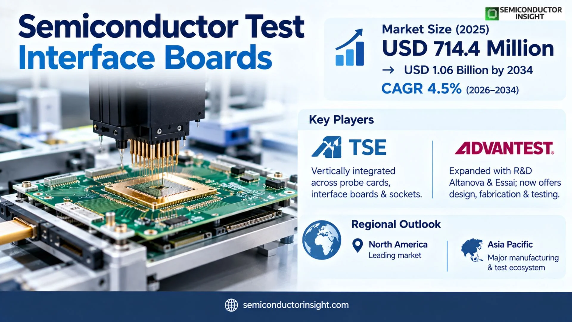
- Test interfaces are becoming vertically integrated. TSE markets a three-part architecture combining probe cards, interface boards and test sockets, while Advantest offers board design, fabrication, assembly and substrates within its interconnect solutions business.
Semiconductor Test Interface Boards Market Overview
Semiconductor Test Interface Boards market is valued at USD 714.4 million in 2025 and is projected to reach USD 1.06 billion by 2034, representing a 4.5% CAGR during 2026–2034. The 2026 estimated market size is USD 746.7 million. North America is the leading regional market in this overview, while Asia Pacific remains a major manufacturing and semiconductor-test ecosystem.
Semiconductor test interface boards connect automated test equipment to the device under test. The category includes probe cards for wafer sort, load boards for packaged-device final test and burn-in boards for reliability screening. These interfaces route thousands of signals, power rails and high-speed channels while maintaining mechanical rigidity, controlled impedance and repeatable contact.
Board complexity rises with semiconductor performance. AI accelerators, CPUs, GPUs, HBM, advanced memory and high-speed networking devices require more pins, higher current and faster serial interfaces. That makes PCB stack-up, via architecture, materials, socket integration, thermal design and signal/power integrity increasingly important to test accuracy.
Customization is inherent to the market because each tester platform, device package and test strategy has different electrical and mechanical requirements. Suppliers therefore compete on engineering speed, simulation capability, in-house PCB fabrication, assembly, test-socket integration and the ability to support customer revisions during rapid device ramps.
Segment Analysis: By Type
By type, the market is segmented into Probe Card, Load Board and Burn-in Board. Probe cards support wafer-level electrical contact, load boards interface packaged devices to final-test handlers and ATE, and burn-in boards carry devices through extended temperature and stress testing.
| Type | Test stage | Market role |
|---|---|---|
| Probe Card | Provides temporary electrical contact between wafer pads or microbumps and automated test equipment. Advanced cards can contain thousands of probes, high-density routing and thermal/mechanical compensation. | Critical for wafer sort, known-good-die and HBM/advanced-package test. Growth is supported by fine-pitch microbumps, higher site count and greater wafer-test value. |
| Load Board | A high-performance PCB positioned between packaged devices and ATE. It integrates sockets, relays, passive components, calibration structures and high-speed signal paths. | Core final-test interface. CPU, GPU, AP, RF and memory devices require customized SI/PI design and strong mechanical support. |
| Burn-in Board | Carries many packaged devices through elevated temperature, voltage and long-duration stress to screen early-life failures. Board materials and sockets must tolerate thermal cycling and repeated insertion. | A reliability-focused segment used heavily in automotive, industrial, memory and mission-critical semiconductors. |
Test stage and device-class segmentation
The market can also be segmented by test stage and device class. Wafer sort is becoming more valuable as advanced packaging makes known-good-die essential, while final test and system-level test validate packaged-device performance. AI/HPC and memory interfaces require especially high pin count, current density and bandwidth.
| Axis | Segments | Commercial implication |
|---|---|---|
| By Test Stage | Wafer Sort · Final Test · Burn-In / Reliability · System-Level Test | Wafer sort reduces packaging scrap, final test verifies packaged devices, burn-in screens reliability and SLT checks operation closer to real application conditions. |
| By Device Class | AI / HPC · Memory / HBM · Mobile / Consumer · Automotive / Power · RF / Connectivity | AI and HBM push pin count and speed; automotive raises reliability and temperature requirements; RF and connectivity demand tighter signal integrity. |
Segment Analysis: By Application
By application, the market serves Consumer Electronics, Automotive, Industrial, Defense & Aerospace and Others. Consumer devices create high unit volume, while automotive, AI/HPC and defense products support higher interface value because of complexity, reliability and qualification requirements.
| Application | Key market insight |
|---|---|
| Consumer Electronics | Mobile processors, application processors, connectivity chips and consumer SoCs require high-throughput final test. Parallel testing and compact load-board layouts reduce cost per device in high-volume production. |
| Automotive | MCUs, PMICs, radar, sensors and power semiconductors require wider temperature ranges and stronger reliability screening. Burn-in and final-test boards must support long qualification cycles and repeated high-temperature operation. |
| Industrial | Industrial controllers, sensors and power devices value stable test coverage, long lifecycle and robust interfaces. Production volumes can be lower than consumer devices but remain active for many years. |
| Defense & Aerospace | Mission-critical devices use stringent electrical and reliability test. Boards may require special materials, low-volume customization and extensive traceability. |
| AI / HPC & Advanced Packaging | Accelerators, CPUs, HBM and chiplets raise interface bandwidth, current and parallelism. Known-good-die test is increasingly important because one bad die can scrap an expensive multi-die package. |
Regional Analysis
North America is the leading regional market in this overview through advanced semiconductor design, high-value ATE and test development, and strong AI/HPC demand. Asia Pacific remains central to production test because Taiwan, South Korea, China, Japan and Southeast Asia contain major foundries, memory manufacturers and OSATs.
How do regional test-interface requirements differ?
North America drives advanced device and test-platform requirements, Asia Pacific has the largest concentration of production test, Europe emphasizes automotive, industrial and power semiconductors, and emerging regions are tied to packaging and assembly investment. Interface-board suppliers often place engineering teams close to customer fabs and OSAT sites because each board is customized.
| Region | Market position | Growth outlook | Core demand | Commercial priority |
|---|---|---|---|---|
| North America | Leading high-value market | High | AI, HPC & ATE development | Bandwidth, power integrity and fast engineering |
| Asia Pacific | Largest production-test ecosystem | Very high | Foundry, memory & OSAT | Scale, parallelism and local support |
| Europe | Automotive / industrial hub | Moderate to high | Auto, power & industrial | Reliability, temperature and lifecycle |
| South America | Small | Selective | Assembly / research | Imported test infrastructure |
| Middle East & Africa | Emerging | Selective | Existing fabs / future projects | Local ecosystem and technical support |
Competitive Landscape
Key participants include TSE, Gorilla Circuits, Corad Technology, Fastprint, Ace Tech Circuit, STK Technology, Abrel, R&D Altanova, Keystone Microtech, ESA Electronics, Venture, Lensuo Technology, CHPT, Zen Voce, Cheer Time Enterprise, ProbeLeader, PRS Electronic, TwinSolution, Semiroc, Sunshine Global Circuits, MemsFlex, ZENFOCUS and Eagle Driver. Competition is fragmented by board type, test platform and geography.
TSE is strongly vertically integrated across probe cards, interface boards and test sockets. Its current i3unify approach is designed to reduce signal-path inconsistency and mechanical mismatch by developing the three key interconnection elements under one system architecture. The company’s 2025 filing shows interface boards were a material part of parent-company revenue.
Advantest acquired R&D Altanova and Essai to expand test-interface boards, substrates, sockets and thermal control within its interconnect business. The company now provides design, PCB fabrication, assembly and electrical verification, giving customers a direct interface between ATE platform and customized DUT hardware.
Keystone Microtech is increasing its role in advanced probing through partnership with FormFactor. Other suppliers compete through quick-turn PCB fabrication, tester-specific design libraries, burn-in expertise, regional cost advantages and customer engineering support.
Competitive tier structure
| Competitive tier | Representative companies | Competitive strengths |
|---|---|---|
| Integrated test-interface leaders | TSE; Advantest / R&D Altanova; Keystone Microtech | Probe cards, interface boards, sockets, substrates, ATE integration and advanced device support |
| PCB / board specialists | Gorilla Circuits; Fastprint; Ace Tech Circuit; STK Technology; Sunshine Global Circuits | High-layer-count PCB fabrication, quick-turn engineering and load-board manufacturing |
| Regional / niche suppliers | Corad; Abrel; ESA; Venture; CHPT; ProbeLeader; ZENFOCUS; others | Tester-specific interfaces, burn-in, regional support and lower-volume customization |
Key companies profiled
Test Interface Board Capacity & Engineering Analysis
Capacity depends on high-layer-count PCB fabrication, advanced materials, via drilling, plating, assembly, socket integration, mechanical frames, simulation and final electrical verification. Unlike commodity PCBs, every interface board is closely tied to a device and tester platform, so engineering throughput can be as important as factory panel capacity.
High-speed boards require low-loss laminates, controlled impedance, dense via structures and careful return-path design. AI and high-speed memory can increase board thickness, layer count and component density, while high-current devices need stronger power planes and cooling.
Repair and revision capability is commercially important because semiconductor programs change during ramp. A board supplier that can modify routing, components or mechanical interfaces quickly helps the customer avoid waiting for a completely new test hardware set.
Market Dynamics
Growth is driven by AI/HPC, advanced packaging, HBM, semiconductor test automation and greater device complexity. Restraints include customization cost, signal-integrity difficulty, long debug cycles and lack of standardization. Opportunities center on fine-pitch probing, 224G/448G test paths, multi-site parallelism and vertically integrated test interfaces.
MARKET DRIVERS
AI devices increase pin count and power
Large accelerators and advanced packages need many high-speed lanes and high-current rails. Interface boards must carry those signals without adding unacceptable loss or voltage drop.
Known-good-die increases wafer-test value
Advanced packages combine several expensive dies. Better wafer-level test reduces the risk of assembling a bad die into a high-value package, increasing demand for sophisticated probe cards and interfaces.
Memory interfaces are getting faster
GDDR7, LPDDR6, DDR6 and HBM push timing and SI requirements. Test hardware becomes a measurable part of the signal path rather than a passive connection.
Automation increases test parallelism
Testing more sites simultaneously reduces cost per device but requires more board area, tester resources and robust routing. Advantest’s DUT Scale Duo addresses this need with more usable DUT-board space.
Drivers Impact Analysis
| Driver | Impact | Primary markets | Time horizon |
|---|---|---|---|
| AI / HPC device complexity | High | North America, Asia Pacific | Short to long term |
| HBM / advanced packaging | High | Taiwan, Korea, U.S. | Medium to long term |
| Automated high-volume test | High | Global OSAT / fabs | Persistent |
| Automotive semiconductor growth | Medium to high | Europe, Asia, North America | Persistent |
MARKET RESTRAINTS
Every device can require a unique interface
Package pinout, socket, tester channel mapping and mechanical constraints vary. This limits manufacturing scale compared with standard PCBs.
High-speed routing leaves little margin
Connector, socket, via and trace discontinuities can distort signals. Simulation and measurement are required before production approval.
Board changes can delay silicon ramps
A layout error or socket change can require redesign and fabrication. Quick-turn capability is therefore critical but expensive.
Tester ecosystems are not fully interchangeable
V93000, UltraFLEX, J750, T2000 and other platforms use different interface and resource architectures, requiring supplier-specific design knowledge.
Restraints Impact Analysis
| Restraint | Impact | Exposure | Time horizon |
|---|---|---|---|
| Customization cost | High | All customers | Persistent |
| Signal / power integrity complexity | High | AI, RF & memory | Persistent |
| Long debug / revision cycles | Medium to high | New device ramps | Short to medium term |
| Limited standardization | Medium | Global | Persistent |
MARKET OPPORTUNITIES
Scale HBM and microbump probing
Fine-pitch advanced packaging increases demand for high-density probe cards and supporting interface boards.
Support 224G and future high-speed links
Networking and AI devices need test paths with much tighter loss and crosstalk budgets, creating premium engineering demand.
Integrate board, probe and socket design
Vertically integrated solutions can reduce interface mismatches and shorten debug time.
Expand automated design-to-test workflows
EDA integration and digital validation can reduce manual board design and improve first-pass success.
Semiconductor Test Interface Board Value Chain Analysis
ATE / device requirements
PCB / substrate design
Fabrication / assembly
ATE qualification / production test
Test strategy defines interface complexity
Site count, test frequency, current and thermal requirements determine board area, layer count and socket arrangement.
Simulation reduces first-pass risk
SI/PI analysis identifies crosstalk, impedance and voltage-drop issues before expensive board fabrication.
Assembly quality protects measurement accuracy
Solder joints, connectors and sockets become part of the test path. Poor assembly can look like device failure or reduce test yield.
Correlation embeds the board into production
Once the interface is correlated to golden devices and tester limits, changing hardware requires controlled validation, creating customer retention.
Recent Developments in the Semiconductor Test Interface Boards Market
Advantest presents advanced test technologies at SEMICON Taiwan 2026
Advantest outlined current work in AI, HPC, silicon photonics and next-generation semiconductor test, reinforcing rising interface complexity around leading-edge devices.
FormFactor and Keystone Microtech expand strategic partnership
The companies expanded probe-card manufacturing and regional support to address AI, HBM, advanced packaging and high-speed semiconductor test requirements.
Advantest expands SiConic into DFT engineering
The new environment lets DFT engineers execute and debug test content in a production-aligned V93000 workflow before manufacturing deployment.
FormFactor advances high-volume microbump probing
FormFactor and Intel Foundry presented production experience for microbump probing in 3D and 2.5D advanced packages, including Foveros and EMIB architectures.
Advantest partners with OpenLight on silicon-photonics test
The partnership targets scalable, high-volume electro-optical test for next-generation optical engines and AI interconnect.
REPORT SCOPE & SEGMENTATION
| Attribute | Details |
|---|---|
| Study Period | 2019–2034 |
| Base Year | 2025 |
| Estimated Year | 2026 |
| Forecast Period | 2026–2034 |
| Historical Period | 2019–2025 |
| Market Size 2025 | USD 714.4 million |
| Market Size 2034 | USD 1.06 billion |
| Growth Rate | 4.5% during 2026–2034 |
| Unit | Value (USD Million/Billion) and interface-board unit shipments |
| By Type | Probe Card · Load Board · Burn-in Board |
| By Application | Consumer Electronics · Automotive · Industrial · Defense and Aerospace · Others |
| By Test Stage | Wafer Sort · Final Test · Burn-In / Reliability · System-Level Test |
| By Device Class | AI / HPC · Memory / HBM · Mobile / Consumer · Automotive / Power · RF / Connectivity |
| By Region | Each region analysed by board type, application, test stage, device class and country market North AmericaUnited States, Canada, Mexico EuropeGermany, France, Italy, United Kingdom and other European markets Asia PacificSouth Korea, Taiwan, China, Japan, Southeast Asia, India and other Asian markets South AmericaBrazil, Argentina and other South American markets Middle East & AfricaIsrael, Saudi Arabia, UAE, South Africa and other MEA markets |
| Key Companies Profiled | TSE · Gorilla Circuits Inc. · Corad Technology · Fastprint · Ace Tech Circuit · STK Technology · Abrel · R&D Altanova / Advantest · Keystone Microtech · ESA Electronics · Venture · Lensuo Technology · CHPT · Zen Voce Corporation · Cheer Time Enterprise · ProbeLeader · PRS Electronic · TwinSolution · Semiroc · Sunshine Global Circuits · MemsFlex · ZENFOCUS · Eagle Driver |
| Customization Scope | Free report customization equivalent to up to four analyst working days with purchase. Addition or alteration to country, regional and segment scope. |
Frequently Asked Questions
What is the 2025 size of the Semiconductor Test Interface Boards market?
The market is valued at USD 714.4 million in 2025 and is projected to reach USD 1.06 billion by 2034. The 2026 estimate is USD 746.7 million and the 2026–2034 CAGR is 4.5%.
Which interface-board types are covered?
The market covers probe cards, load boards and burn-in boards used across wafer sort, packaged-device final test and reliability screening.
Which applications drive demand?
Consumer electronics, automotive, industrial, defense and aerospace all contribute, while AI/HPC and HBM are increasing technical complexity and interface value.
Which region leads the market?
North America is used as the leading regional market in this overview, supported by advanced semiconductor design, ATE development and high-value test infrastructure.
What is the estimated market size in 2026?
The 2026 estimated market size is USD 746.7 million, based on the endpoint-consistent growth path from the 2023 and 2030 global values.
Why are test interface boards customized?
Each semiconductor device has a unique package, pinout, test program, current demand and tester-channel mapping, requiring dedicated electrical and mechanical design.
How is AI changing interface boards?
AI accelerators need more pins, higher current, faster data links and advanced packaging. This increases board layer count, SI/PI requirements and the need for known-good-die test.
What are the main market restraints?
High customization cost, signal-integrity complexity, long debug cycles and limited standardization across tester platforms are the main constraints.
Which companies are active in the market?
Key companies include TSE, R&D Altanova/Advantest, Keystone Microtech, Gorilla Circuits, Fastprint, Ace Tech Circuit and a broad group of regional test-interface suppliers.
What does the report cover?
The report covers probe cards, load boards and burn-in boards; applications and device classes; regional markets; competitive landscape; capacity; market dynamics; recent developments and value chain.
Research Sources & Evidence Base
View primary and authoritative evidence used in this overview
- Advantest. Test Interface Boards – Official product information on design, fabrication, load boards, MLO substrates, assembly and test.
- Advantest. V93000 DUT Board Design Guide – Official technical support for DUT boards, prober interface boards and probe cards.
- SEMI. TSE Company Profile – Industry association profile identifying TSE as a semiconductor test-interface company.
- SEMICON Taiwan. TSE 2026 Exhibitor Profile – Current evidence on TSE probe cards, interface boards, test sockets and integrated i3unify architecture.
- FormFactor. FormFactor–Keystone Microtech Partnership – July 2026 evidence on advanced probe-card manufacturing for AI, HBM and advanced packaging.
- FormFactor. Advanced HBM / Memory Wafer Test – Official technical evidence on known-good-die, high-speed memory and advanced-package wafer test.
Get Sample Report PDF for Exclusive Insights
Report Sample Includes
- Table of Contents
- List of Tables & Figures
- Charts, Research Methodology, and more...