
Key Statistics
Key Takeaways
- Rigid PCBs remain the largest type by broad installed demand, while HDI and substrate-like PCBs gain value as device density, signal speed and packaging complexity rise.
- Consumer electronics remains the largest application by unit volume, while automotive, AI servers and telecom infrastructure are increasing the mix of multilayer, high-frequency and high-reliability boards.
- Asia Pacific leads the market through the concentration of PCB fabrication, electronics manufacturing, substrate production and component assembly across China, Japan, South Korea, Taiwan and Southeast Asia.
- HDI is a central technology shift because finer lines, microvias and sequential lamination allow more interconnect density within smaller footprints and are increasingly required by defense, mobile and AI hardware.
- AI data centers are raising PCB requirements through faster SerDes, larger multilayer counts, low-loss laminates and high-current power delivery, increasing the value of advanced board materials and process control.
- Sustainability is becoming operational as manufacturers invest in lower-waste fabrication, precious-metal recovery and tighter environmental controls across plating, etching and end-of-life electronics.
Printed Circuit Boards (PCBs) Market Overview
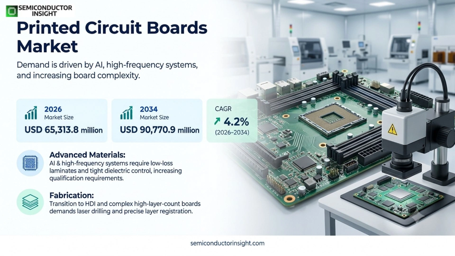
Printed Circuit Boards Market was valued at USD 62,681.2 million in 2025, is estimated at USD 65,313.8 million in 2026, and is projected to reach USD 90,770.9 million by 2034, representing a CAGR of 4.2% during 2026–2034. Asia Pacific is the largest regional market in 2025, while the commercial growth mechanism is increasingly shaped by AI servers, high-density interconnect, vehicle electrification, 5G infrastructure, rigid-flex adoption, and advanced packaging.
Printed circuit boards are the physical interconnect platform that mechanically supports and electrically connects electronic components through patterned copper conductors, vias, pads and dielectric layers. The market includes rigid, flexible, rigid-flex, high-density interconnect and substrate-like boards ranging from simple two-layer products to complex multilayer structures used in servers, radar, vehicles, medical equipment and telecom systems.
Technical requirements are rising faster than simple board unit volumes. AI accelerators and networking systems need low-loss materials and precise impedance at very high data rates; vehicles require thermal cycling, vibration resistance and long service life; smartphones and wearables continue pushing finer lines and microvias; and aerospace and defense programs need domestic, trusted production with high layer counts and controlled materials. These requirements shift revenue toward more complex board architectures.
Manufacturing economics depend on yield across imaging, lamination, drilling, plating, etching and test. A high-layer-count HDI board can pass through repeated build-up cycles, so a defect late in the process can destroy substantial accumulated value. Suppliers with advanced laser drilling, automated optical inspection, process analytics and strong material control are therefore better positioned in premium applications than producers focused only on commodity board area.
Segment Analysis: By Type
By type, the market includes Rigid PCBs, Flexible PCBs, Rigid-Flex PCBs, High-Density Interconnect (HDI) PCBs, Substrate-like PCBs (SLP), and Other specialized boards. Rigid boards hold the broadest installed base, while HDI and rigid-flex are among the most strategically important growth categories.
| Type | Technical role | Market position |
|---|---|---|
| Rigid PCBs | Use rigid dielectric laminates and copper layers to provide mechanical support and stable routing in consumer, industrial, telecom, automotive and computing equipment. | The largest type by broad market volume. Growth is strongest in multilayer, high-speed and high-power designs rather than simple commodity boards. |
| Flexible PCBs | Use flexible polymer substrates to route signals through compact or moving assemblies where rigid boards would consume too much space or fail under repeated bending. | Important in mobile devices, wearables, cameras, automotive modules and medical devices; value rises with finer features and complex multilayer flex. |
| Rigid-Flex PCBs | Combine rigid component areas with integrated flexible interconnect, removing connectors and cables while allowing complex three-dimensional packaging. | A high-value segment in aerospace, medical, automotive and compact electronics where reliability and space savings justify higher fabrication complexity. |
| HDI PCBs | Use microvias, fine lines, thin dielectrics and sequential build-up layers to increase routing density and shorten interconnect length. | A major growth category for smartphones, AI servers, defense electronics and advanced networking where conventional through-hole routing cannot meet density targets. |
| Substrate-like PCBs (SLP) | Use very fine line/space dimensions that approach IC-substrate processes and enable dense packaging between conventional PCB and semiconductor substrate technologies. | A strategic segment tied to premium mobile devices and increasingly complex compact electronics. |
| Others | Includes high-frequency, heavy-copper, metal-core, thick-film and other specialty board constructions. | Smaller individual markets but high value where RF loss, thermal handling, current capacity or environmental durability matter. |
Why does HDI create higher manufacturing value?
HDI boards require laser-drilled microvias, tighter registration, sequential lamination and finer imaging than conventional multilayer PCBs. Each additional build-up cycle adds processing and inspection steps, but it enables shorter signal paths, more routing layers and smaller finished products. AI servers, radar, mobile devices and advanced defense electronics increasingly need these capabilities, allowing qualified HDI manufacturers to capture higher value per square meter than standard board producers.
Segment Analysis: By Application
By application, the market spans Consumer Electronics, Automotive, Industrial, Medical Devices, Aerospace & Defense, and Telecommunications. Consumer electronics remains the largest broad volume application, while automotive, aerospace/defense and AI-related computing are driving richer product mix.
| Application | Demand characteristics | |
|---|---|---|
| Consumer Electronics | Smartphones, notebooks, televisions, wearables and connected devices use large volumes of multilayer, flex and HDI boards. Product cycles are short and cost pressure is intense. | The largest unit-volume application and a major driver of HDI, flex and substrate-like PCB technology. |
| Automotive | ADAS, infotainment, battery management, power electronics and zonal controllers require high-reliability boards that withstand heat, vibration and long operating life. | A strong growth market with increasing PCB value per vehicle as electrification and software-defined architectures expand. |
| Industrial | Automation, robotics, motor drives, test equipment and power systems use multilayer, heavy-copper and high-reliability boards. | A stable premium application where long lifecycle and field reliability matter more than consumer-style price minimization. |
| Medical Devices | Imaging, diagnostics, wearables and surgical systems use compact rigid-flex and high-reliability assemblies with strict traceability. | A smaller but high-value segment where supplier qualification and documentation create switching costs. |
| Aerospace & Defense | Radar, avionics, missiles, satellites and secure communications require high-layer-count, RF and rugged PCB technologies. | A high-value segment benefiting from domestic capacity investment and trusted-supply requirements. |
| Telecommunications | 5G radios, routers, switches and optical networking equipment use high-frequency, low-loss and multilayer boards. | Growth follows network bandwidth and data-center connectivity, with material performance becoming increasingly important. |
Why are AI servers changing the PCB mix?
AI servers combine high-speed serial links, dense accelerator modules, large current delivery and complex cooling. Motherboards and switch boards therefore use more layers, tighter impedance control and lower-loss laminates than conventional enterprise equipment. IPC has highlighted PCB design, HDI fabrication and PCBA assembly as critical parts of a resilient AI server supply chain. This raises the value of advanced PCB capability even when server unit volumes are far below consumer-electronics shipments.
Regional Analysis
Asia Pacific leads the Printed Circuit Boards market through the world’s largest concentration of PCB fabrication, electronics manufacturing and substrate ecosystems. North America is strengthening domestic advanced-board capability for defense and AI infrastructure, while Europe remains important in automotive, industrial and medical electronics.
How do regional PCB markets differ?
Asia Pacific competes on scale, technology breadth and proximity to electronics OEMs. North America places greater weight on trusted supply, defense-grade HDI and high-mix advanced electronics. Europe is led by automotive, industrial and medical applications and is also adding advanced substrate capacity. South America remains import dependent, while the Middle East and Africa consume PCBs mainly through telecom, industrial and smart-infrastructure systems.
| Region | Position | Growth outlook | Demand profile | What decides supplier selection |
|---|---|---|---|---|
| Asia Pacific | Largest | Strong | Consumer, server, automotive and telecom manufacturing | Scale, yield, fine-line capability and local supply |
| North America | Premium domestic-capacity market | Strong | Defense, aerospace, AI servers and medical | Trusted supply, Ultra-HDI, quality and lifecycle support |
| Europe | Automotive & industrial specialist | Moderate to strong | Automotive, medical and industrial electronics | Reliability, local production and advanced materials |
| South America | Smaller import-dependent market | Selective | Automotive, industrial and consumer assembly | Landed cost, distributor access and local assembly |
| Middle East & Africa | Emerging application market | Selective | Telecom, infrastructure, defense and electronics localization | System integration and supply availability |
Competitive Landscape
Key participants include AT&S, Nippon Mektron, Unimicron, Samsung Electro-Mechanics, Dynamic Electronics, Daeduck Electronics, CMK, Nan Ya PCB, TTM Technologies and Shenzhen Kinwong Electronic. Competition is fragmented by technology, geography and end market.
Unimicron, Nan Ya PCB, Daeduck and Asian peers benefit from proximity to semiconductor, server and consumer-electronics ecosystems. Their scale allows investment in HDI, fine-line and substrate-adjacent technologies while serving large OEM programs.
TTM Technologies is differentiated by aerospace, defense and high-technology interconnect, and its 2026 Syracuse Ultra-HDI facility strengthens domestic U.S. capability. AT&S competes at the high end through advanced PCBs and IC substrates, including expansion in Kulim to serve AI-related demand.
Nippon Mektron remains a major flexible-circuit participant, while regional specialists compete in rigid, rigid-flex and high-frequency niches. The market rewards suppliers able to combine material expertise, high yield, fast engineering turns and geographically diversified production.
| Competitive tier | Representative companies | Commercial basis |
|---|---|---|
| Advanced global leaders | AT&S; Unimicron; TTM Technologies; Nan Ya PCB | HDI, high-layer-count, substrates, advanced materials and large global customer programs. |
| Asian scale suppliers | Nippon Mektron; Samsung Electro-Mechanics; Daeduck Electronics; Dynamic Electronics | High-volume production, mobile, automotive, computing and flexible-board capability. |
| Regional and specialist manufacturers | CMK Corporation; Shenzhen Kinwong Electronic | Automotive, industrial and cost-competitive regional production. |
Key Market Participants
AT&S, Nippon Mektron, Unimicron, Samsung Electro-Mechanics, Dynamic Electronics, Daeduck Electronics, CMK Corporation, Nan Ya PCB, TTM Technologies, Shenzhen Kinwong Electronic.
Production Capacity Analysis
PCB production is a multi-stage chemical and mechanical process involving laminate preparation, imaging, drilling, copper plating, etching, lamination, solder mask, surface finish and electrical test. Advanced HDI adds laser microvias and repeated build-up cycles, increasing both capital intensity and yield sensitivity.
Raw materials include copper foil, glass fiber, epoxy or other dielectric systems, specialty low-loss laminates, films and plating chemicals. AI and high-frequency systems require materials with tighter dielectric properties and lower signal loss, increasing supplier qualification requirements.
Fabrication converts the laminate stack into conductive circuitry through imaging, etching and via formation. HDI uses laser drilling and sequential lamination, while high-layer-count boards require precise registration across many copper and dielectric layers.
Final inspection combines automated optical inspection, electrical test and reliability checks. AI-based AOI is increasingly used to improve defect classification and reduce false calls, while high-reliability sectors add traceability, microsectioning and environmental testing.
| Capacity layer | Where it concentrates | Commercial constraint |
|---|---|---|
| Laminates, copper foil & chemicals | Asia Pacific, Europe and North America | Low-loss dielectric quality, copper profile and material availability. |
| Imaging, drilling & plating | China, Taiwan, Japan, Korea, Southeast Asia, U.S. and Europe | Line/space capability, microvia yield, layer registration and plating uniformity. |
| Lamination & surface finish | Major PCB manufacturing hubs | Warpage, adhesion, thickness control and finish quality. |
| Inspection & test | Integrated within PCB plants worldwide | AOI accuracy, electrical test coverage and high-reliability qualification. |
Market Dynamics
The PCB market is driven by more electronic content and increasing interconnect complexity. Revenue growth is strongest where boards move from standard multilayer products toward HDI, high-frequency, rigid-flex and substrate-like designs. Commodity pricing, materials volatility and environmental compliance remain persistent constraints.
Market Drivers
| Factor | Directional impact | Why it matters |
|---|---|---|
| AI servers and high-speed networking | High | Higher data rates require low-loss multilayer boards and more advanced HDI routing. |
| Vehicle electrification and ADAS | High | More ECUs, sensors, inverters and battery systems increase PCB value per vehicle. |
| 5G and wireless systems | Medium-High | RF equipment requires high-frequency materials and tight impedance control. |
| Miniaturization and rigid-flex adoption | Medium-High | Compact products use finer lines, microvias and flexible interconnect. |
AI servers increase board complexity
Accelerator systems require high-speed signaling and high-current power delivery, raising layer count, material performance and via density. This shifts demand toward advanced PCB suppliers with low-loss laminates and reliable HDI processes.
Automotive electronics expands board content
EVs and software-defined vehicles use more battery, sensing, infotainment and control electronics. Automotive qualification and long lifecycles support higher-value PCBs and stable supplier relationships.
5G and connectivity raise RF requirements
High-frequency radios and network equipment require controlled impedance and low dielectric loss. Material selection becomes a system-performance issue rather than a commodity purchasing decision.
Miniaturization drives finer routing
Smaller products and denser component packages require microvias and finer lines. HDI allows designers to reduce board area while maintaining connectivity, increasing process value per unit area.
Market Restraints
| Factor | Directional impact | Why it matters |
|---|---|---|
| Advanced fabrication cost | High | HDI and high-layer-count boards require laser drilling, sequential lamination and extensive inspection. |
| Raw-material and copper volatility | Medium-High | Copper foil, laminates and specialty chemicals can pressure margins. |
| Environmental compliance | Medium | Plating, etching and waste treatment require capital and strict process control. |
| Yield loss at high complexity | High | Late-stage defects can destroy substantial accumulated value on complex multilayer boards. |
Complex boards are capital intensive
Advanced HDI lines need laser drilling, direct imaging and precise plating equipment. Smaller manufacturers may struggle to justify investment without long-term customer programs.
Material volatility affects contract pricing
Copper and specialty laminates can move significantly in price, while customer agreements may limit immediate pass-through. Long-term sourcing and material standardization help protect margins.
Environmental controls add operating cost
PCB fabrication uses chemicals and water across plating and etching. Wastewater treatment, emissions controls and recycling requirements raise capital needs but are essential to operating permits and customer ESG expectations.
Yield becomes harder at finer geometry
Every added lamination cycle and microvia layer creates another opportunity for misregistration, voids or opens. Inspection and process analytics are therefore central to profitable advanced PCB production.
Market Opportunities
Ultra-HDI for defense and AI
Fine-line, microvia and high-layer-count capability can address defense, AI servers and advanced networking where domestic or trusted supply is strategic.
Advanced PCBs and IC-substrate convergence
Substrate-like boards and core technologies sit between traditional PCBs and semiconductor packaging, creating growth around chiplets and high-performance compute.
Rigid-flex medical and automotive
Space savings and connector reduction improve reliability in compact high-value systems, supporting premium pricing.
Circular PCB materials and recovery
Precious-metal recovery and improved recycling can reduce waste and create new value streams from end-of-life electronics.
Supply Chain Analysis
Materials. Advanced boards require stable dielectric constant, low loss and reliable copper adhesion. Material qualification can take months, so major fabricators maintain close relationships with laminate and foil suppliers.
Board Fabrication. Factories combine wet chemistry with precision imaging and drilling. HDI adds sequential build-up and microvias, increasing process steps and making yield management the central economic variable.
Finish & Test. ENIG and other surface finishes protect exposed copper and support solderability. AOI and electrical tests screen opens, shorts and imaging defects before expensive components are assembled.
PCBA & OEM Integration. Boards move to EMS or OEM plants for solder paste, component placement and reflow. Design feedback from assembly can influence pad geometry, warpage limits and panelization in the next PCB revision.
Recent Developments in the Printed Circuit Boards (PCBs) Market
Developments tracked to September 2026. Entries are dated to the official publication date where available.
- 22 June 2026 Capacity
TTM Technologies opened a new Ultra-HDI PCB manufacturing facility in Syracuse, New York. The $130 million investment supports advanced defense electronics including radar, missile defense, space and autonomous systems. Source - 17 June 2026 M&A
TTM Technologies announced agreements to acquire Swiss Technology Group and ILFA. The transactions would add European rigid, flex, rigid-flex, multilayer and medical/defense PCB capability. Source - 15 June 2026 Expansion
AT&S announced expansion of its Kulim site for IC substrate cores and advanced PCBs. The investment is backed by long-term customer commitments and targets sustained AI-driven demand. Source - 6 February 2025 Manufacturing AI
IPC released a white paper on AI in automated optical inspection for electronics manufacturing. Improved inspection accuracy can support higher yields as PCB and PCBA complexity rises. Source - 2024–2026 Circular economy
The Royal Mint scaled a facility capable of processing up to 4,000 tonnes of PCBs from e-waste each year. The operation recovers gold and other materials from discarded electronics. Source
Report Scope & Segmentation
| Attribute | Coverage |
|---|---|
| Report title | Printed Circuit Boards (PCBs) Market, Size, Trends, Business Strategies 2025-2032 |
| Base / estimate / forecast | 2025 base year; 2026 estimated year; 2034 forecast end year; CAGR measured for 2026–2034. |
| By Type | Rigid PCBs; Flexible PCBs; Rigid-Flex PCBs; High-Density Interconnect (HDI) PCBs; Substrate-like PCBs (SLP); Others |
| By Application | Consumer Electronics; Automotive; Industrial; Medical Devices; Aerospace & Defense; Telecommunications |
| By Layer Count | Single-Sided; Double-Sided; Multilayer (4-6 Layer, 8-16 Layer, 16+ Layer) |
| By End-User Industry | Electronics Manufacturing Services (EMS); Original Equipment Manufacturers (OEMs); PCB Fabrication Companies |
| Regions | North America, Europe, Asia-Pacific, South America, and Middle East & Africa, with country-level analysis across the principal national markets. |
| Companies | AT&S, Nippon Mektron, Unimicron, Samsung Electro-Mechanics, Dynamic Electronics, Daeduck Electronics, CMK Corporation, Nan Ya PCB, TTM Technologies, Shenzhen Kinwong Electronic |
| Customization Scope | Free report customization (equivalent to up to 4 analyst working days) with purchase. Addition or alteration to country,regional and segment scope. |
Frequently Asked Questions
What is the size of the Printed Circuit Boards market?
The global PCB market is valued at USD 62,681.2 million in 2025, is estimated at USD 65,313.8 million in 2026, and is projected to reach USD 90,770.9 million by 2034, representing a 4.2% CAGR during 2026–2034.
Which region leads the PCB market?
Asia Pacific leads because the region contains the world’s largest PCB fabrication and electronics-manufacturing base, including major suppliers in China, Taiwan, Japan and South Korea.
Which PCB type is largest?
Rigid PCBs have the broadest installed demand, while HDI, rigid-flex and substrate-like boards are growing in strategic importance as electronics become denser and faster.
Which application is largest?
Consumer electronics remains the largest broad application by volume, while automotive, AI servers and telecom are increasing demand for higher-value multilayer and high-frequency products.
Why is HDI important?
HDI uses microvias, fine lines and sequential build-up layers to place more routing into a smaller area. It is essential in smartphones, AI servers, defense systems and other dense electronics.
How do AI servers affect PCB demand?
AI servers require higher-speed signaling, more power delivery and greater layer counts, increasing demand for low-loss laminates, tighter impedance control and advanced HDI.
What are the main PCB market restraints?
High advanced-fabrication cost, materials volatility, environmental compliance and yield loss on complex multilayer products are the main constraints.
Who are the major PCB companies?
Key companies include AT&S, Nippon Mektron, Unimicron, Samsung Electro-Mechanics, Dynamic Electronics, Daeduck Electronics, CMK, Nan Ya PCB, TTM Technologies and Shenzhen Kinwong Electronic.
What role does rigid-flex play?
Rigid-flex combines rigid component areas with integrated flexible interconnect, reducing connectors and enabling compact three-dimensional packaging in medical, aerospace, mobile and automotive systems.
Where are the strongest PCB opportunities?
The strongest opportunities are in Ultra-HDI, AI server boards, automotive electronics, advanced substrate-like PCBs, rigid-flex and circular manufacturing.
Research Sources & Evidence Base

Get Sample Report PDF for Exclusive Insights
Report Sample Includes
- Table of Contents
- List of Tables & Figures
- Charts, Research Methodology, and more...
 Download Sample Report PDF





