
Advanced Memory Packaging Market Insights
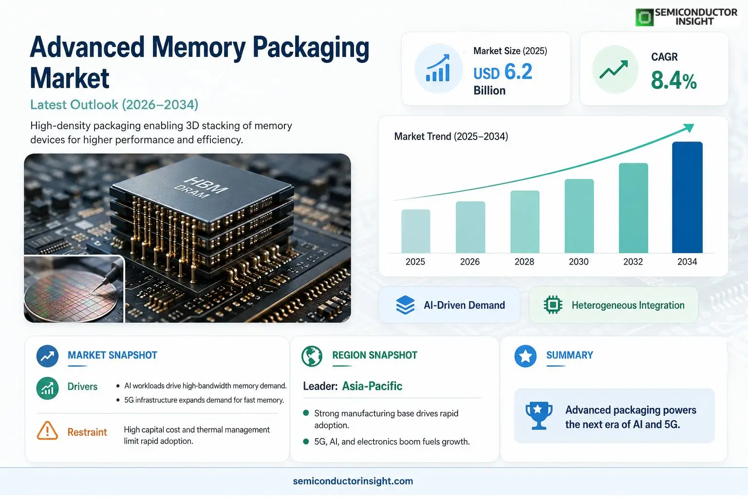
Global Advanced Memory Packaging Market size was valued at USD 6.2 billion in 2025. The market is projected to grow from USD 6.2 billion in 2025 to USD 12.8 billion by 2034, exhibiting a CAGR of 8.4% during the forecast period.
Advanced memory packaging encompasses high‑density interconnect solutions such as through‑silicon vias (TSV), fan‑out wafer‑level packaging (FOWLP), and heterogeneous integration techniques that enable stacking of DRAM, HBM, and emerging memory types while maintaining signal integrity and thermal performance.The market is experiencing rapid growth because AI‑driven workloads, high‑performance computing, and mobile devices demand ever‑higher bandwidth and lower power consumption. Furthermore, investments in semiconductor fabs and the rollout of 5G accelerate adoption of these packaging technologies. Key players such as Samsung Electronics, TSMC, ASE Technology Holding, Amkor Technology, and Intel are expanding their portfolios through strategic partnerships and technology roadmaps.
MARKET DRIVERS
Growing Adoption of AI‑Enabled Edge Devices
The surge in artificial intelligence workloads at the edge is prompting OEMs to seek higher bandwidth and lower latency solutions. Advanced Memory Packaging Market players are benefitting from this shift as stacked‑die and 3D‑TSV technologies enable compact form factors while delivering superior performance.
Expansion of 5G Infrastructure
Deployment of 5G networks is driving demand for high‑speed memory modules in base stations and smartphones. The need for dense interconnects and thermal efficiency positions advanced packaging as a critical enabler.
➤ Industry analysts forecast a double‑digit CAGR for the segment through 2032, reflecting sustained investment in next‑gen packaging.
Manufacturers are also leveraging advanced packaging to meet stringent automotive safety standards, further broadening the addressable market.
MARKET CHALLENGES
High Capital Expenditure for New Fab Lines
Establishing state‑of‑the‑art packaging facilities requires multi‑billion dollar investments, creating entry barriers for smaller firms and slowing overall capacity expansion.
Other Challenges
Process Integration Complexity
Coordinating heterogeneous dies, interposers, and substrate materials demands sophisticated design tools and cross‑disciplinary expertise, increasing time‑to‑market. Supply‑chain volatility for rare‑earth metals used in certain interconnects further compounds the risk profile for adopters.
MARKET RESTRAINTS
Thermal Management Constraints
As memory density rises, effective heat dissipation becomes a limiting factor. Without innovative cooling solutions, yield losses can erode profitability.Regulatory scrutiny over the environmental impact of advanced materials also imposes compliance costs that may deter rapid rollout.Finally, the reliance on highly specialized equipment limits flexibility in scaling production volumes to match sudden demand spikes.
MARKET OPPORTUNITIES
Emergence of Chip‑let Architectures
Chip‑let integration, enabled by high‑density interposers, opens pathways for modular product designs. Companies that master this approach can capture new value streams and differentiate their offerings.Additionally, the convergence of memory and logic in heterogeneous stacking presents opportunities for differentiated performance tiers, especially in autonomous vehicle and augmented reality applications.Strategic collaborations between memory manufacturers and fabless designers are expected to accelerate innovation cycles, further expanding the addressable market.
Advanced Memory Packaging Market Trends
AI‑Driven Demand for High‑Bandwidth Interconnects
Advanced Memory Packaging Market is being reshaped by the exponential growth of artificial‑intelligence workloads. Modern AI models require multi‑terabyte memory pools with extremely low latency, prompting designers to adopt through‑silicon‑via (TSV) and fan‑out wafer‑level (FOWLP) solutions that deliver higher pin counts per square millimeter. Semiconductor fabs are integrating these packaging approaches into their process lines to sustain the rising bandwidth per watt ratios demanded by data‑center accelerators and edge‑inference devices. This shift is evident in the broader industry focus on tighter integration of memory and logic, which reduces signal loss and improves thermal management across complex AI pipelines.
Other Trends
Emergence of Fan‑Out Wafer‑Level Packaging (FOWLP)
FOWLP has gained traction as a cost‑effective alternative to traditional flip‑chip methods, especially for mobile and IoT applications that prioritize form‑factor and power efficiency. By redistributing I/O on a reconstituted wafer, manufacturers can achieve finer pitch interconnects without the need for a separate substrate, leading to thinner modules and faster time‑to‑market. Advanced Memory Packaging Market sees increasing adoption of this technique for LPDDR and emerging memory families, where the combination of reduced parasitic inductance and improved heat spreading aligns with the power‑budget constraints of next‑generation smartphones and wearables.
Shift Toward Heterogeneous Integration
Another prominent trend is the move toward heterogeneous integration, where DRAM, HBM, and emerging non‑volatile memories are stacked alongside compute dies in a single package. This architecture enables designers to tailor memory bandwidth to specific workloads while minimizing the die‑to‑die distance, which is critical for maintaining signal integrity at high frequencies. Leading foundries are offering multi‑chip‑module (MCM) services that bundle memory and logic in a unified substrate, facilitating rapid prototyping and reducing the overall bill of materials. As 5G rollout accelerates and edge computing expands, the need for compact, high‑performance memory solutions will drive further consolidation of these technologies within Advanced Memory Packaging Market.
COMPETITIVE LANDSCAPEKey Industry Players
Strategic Expansion, Technology Innovation, and Heterogeneous Integration Define the Competitive Dynamics of Global Advanced Memory Packaging Market
Global advanced memory packaging market is characterized by intense competition among a select group of vertically integrated semiconductor giants and specialized outsourced semiconductor assembly and test (OSAT) providers. Samsung Electronics commands a formidable position, leveraging its end-to-end capabilities across DRAM manufacturing, High Bandwidth Memory (HBM) development, and advanced packaging technologies including through-silicon vias (TSV) and fan-out wafer-level packaging (FOWLP). TSMC reinforces its competitive standing through its Integrated Fan-Out (InFO) and Chip-on-Wafer-on-Substrate (CoWoS) platforms, which are widely adopted for AI accelerator and high-performance computing applications. Intel further strengthens the competitive landscape with its Foveros 3D stacking and EMIB (Embedded Multi-die Interconnect Bridge) technologies, targeting heterogeneous integration use cases across data center and edge computing segments. SK Hynix has emerged as a critical player in HBM supply chains, particularly for AI GPU platforms, while Micron Technology continues to invest in next-generation memory packaging architectures to capture growing demand from machine learning and inferencing workloads.Beyond the leading integrated players, several specialized and niche companies contribute significantly to the advanced memory packaging ecosystem. ASE Technology Holding and Amkor Technology are the two largest OSAT providers globally, offering a broad portfolio of advanced packaging services including flip-chip, wafer-level packaging, and system-in-package (SiP) solutions to fabless and IDM clients alike. Powertech Technology and JCET Group have also established strong regional footholds, particularly in Asia-Pacific markets, providing cost-competitive packaging services for DRAM and NAND flash memory products. Additionally, Brewer Science and Kulicke and Soffa Industries supply critical materials and equipment that underpin next-generation packaging processes. As AI-driven workloads and 5G deployments continue to accelerate bandwidth and power efficiency requirements, competition is expected to intensify around HBM4 development, chiplet architectures, and thermal management innovations across the forecast period through 2034.
List of Key Advanced Memory Packaging Companies Profiled
- Samsung Electronics Co., Ltd.
- Taiwan Semiconductor Manufacturing Company (TSMC)
- Intel Corporation
- SK Hynix Inc.
- Micron Technology, Inc.
- ASE Technology Holding Co., Ltd.
- Amkor Technology, Inc.
- Powertech Technology Inc.
- JCET Group Co., Ltd.
- Kulicke and Soffa Industries, Inc.
- Brewer Science, Inc.
- Shin-Etsu Chemical Co., Ltd.
- Entegris, Inc.
- Onto Innovation Inc.
- Veeco Instruments Inc.
Segment Analysis:
| Segment Category | Sub-Segments | Key Insights |
| By Type |
|
Through‑Silicon Vias (TSV) is recognized as the leading type due to its ability to provide high‑density vertical interconnects, preserving signal integrity for high‑bandwidth memory stacks.
|
| By Application |
|
AI Accelerators dominate the application landscape as the demand for massive parallel processing drives the adoption of advanced memory packaging.
|
| By End User |
|
Data Center Operators are the primary end‑user segment, driven by the need for high‑throughput memory solutions in AI‑infused cloud services.
|
| By Technology Maturity |
|
Mature Production leads this classification as manufacturers have refined processes that deliver consistent yield and reliability.
|
| By Integration Approach |
|
3D Stacking emerges as the dominant integration approach, offering the highest memory density and performance.
|
Regional Analysis: North America
United States
The United States is driving innovation in areas such as 3D stacking, chiplet integration, and advanced packaging materials. Focus on enhancing data transfer speeds and reducing power consumption remains paramount.
Growing demand from AI, HPC, and data centers, coupled with the increasing complexity of memory systems, are key drivers. Government initiatives promoting semiconductor manufacturing are also contributing to market expansion.
The North American market features a mix of established memory manufacturers and emerging packaging solution providers. Strategic partnerships and collaborations are crucial for success in this competitive environment.
Significant investments are being directed towards research and development, manufacturing capacity expansion, and talent acquisition to support the growing demand for advanced memory packaging.
Europe
Europe represents a significant and steadily growing market for Advanced Memory Packaging. Driven by the strong automotive and industrial sectors, the region is witnessing increasing adoption of advanced memory solutions. Several countries, particularly Germany, France, and the Netherlands, are investing heavily in semiconductor manufacturing and research, fostering a favorable environment for innovation. The emphasis on energy efficiency and sustainable technologies is also influencing the demand for advanced memory packaging. European players are focusing on developing innovative packaging technologies to meet the specific requirements of various applications, including automotive, industrial automation, and high-performance computing. Collaboration between industry, academia, and government is a key strength of the European market. This collaborative ecosystem supports the development and commercialization of cutting-edge memory packaging solutions. The focus is on high reliability and integration within complex systems.
Asia-Pacific
Asia-Pacific is anticipated to become the largest and fastest-growing market for Advanced Memory Packaging. China, Japan, South Korea, and Taiwan are leading the charge, fuelled by rapid expansion in the electronics, telecommunications, and automotive industries. The region’s robust manufacturing capabilities and large-scale investments in semiconductor production are driving demand for advanced memory packaging. Government support for the semiconductor industry is also a significant factor contributing to market growth. The increasing adoption of 5G, IoT, and AI technologies further boosts the demand for high-performance memory solutions. Key players in the region are focusing on expanding their production capacity and developing innovative packaging technologies to cater to the evolving needs of the market. Strong domestic demand and export opportunities are propelling the growth of Advanced Memory Packaging Market in Asia-Pacific.
South America
Advanced Memory Packaging Market in South America is currently in its nascent stages but holds significant potential for growth. The growth is primarily driven by the expanding electronics and telecommunications sectors in countries like Brazil and Argentina. Increasing adoption of smart devices, cloud computing, and industrial automation are creating demand for advanced memory solutions. While the market is relatively fragmented, there is a growing interest in local manufacturing and assembly. However, factors like economic volatility and limited investment in research and development pose challenges to market growth. The region’s potential is closely linked to the continued development of its technological infrastructure and the expansion of its industrial base. The focus is on cost-effective solutions for emerging applications.
Middle East & Africa
The Middle East & Africa represents a smaller but gradually expanding market for Advanced Memory Packaging. The increasing adoption of technology in sectors such as telecommunications, healthcare, and automotive is driving demand. Government initiatives focused on economic diversification and technological advancement are also contributing to market growth. The region is witnessing growing investments in infrastructure projects, which in turn are boosting demand for electronics and associated memory solutions. While the market is relatively price-sensitive, the increasing awareness of advanced memory technologies is creating new opportunities for growth. The focus is on providing reliable and cost-effective memory packaging solutions to meet the specific needs of the region.
Report Scope
This market research report provides a comprehensive analysis of the Advanced Memory Packaging Market , covering the forecast period 2026–2034. It offers detailed insights into market dynamics, technological advancements, competitive landscape, and key trends shaping the industry.
Key focus areas of the report include:
- Market Overview: The report begins with an overview outlining its current market scenario, key growth indicators, and industry transformation drivers. It discusses macroeconomic factors, demand–supply balance, regulatory landscape, and the strategic role of semiconductors in powering advancements across industries such as automotive, telecommunications, consumer electronics, and industrial automation.
- Market Size & Forecast: Historical data and future projections for revenue, unit shipments, and market value across major regions and segments.
- Segmentation Analysis: Detailed breakdown by product type, technology, application, and end-user industry to identify high-growth segments and investment opportunities.
- Regional Insights: Insights into market performance across North America, Europe, Asia-Pacific, Latin America, and the Middle East & Africa, including country-level analysis where relevant.
- Competitive Landscape: Profiles of leading market participants, including their product offerings, R&D focus, manufacturing capacity, pricing strategies, and recent developments such as mergers, acquisitions, and partnerships.
- Technology Trends & Innovation: Assessment of emerging technologies, integration of AI/IoT, semiconductor design trends, fabrication techniques, and evolving industry standards.
- Market Drivers & Restraints: Evaluation of factors driving market growth along with challenges, supply chain constraints, regulatory issues, and market-entry barriers.
- Stakeholder Insights: Insights for component suppliers, OEMs, system integrators, investors, and policymakers regarding the evolving ecosystem and strategic opportunities.
Primary and secondary research methods are employed, including interviews with industry experts, data from verified sources, and real-time market intelligence to ensure the accuracy and reliability of the insights presented.
FREQUENTLY ASKED QUESTIONS:
What is the current market size of Advanced Memory Packaging Market?
-> Advanced Memory Packaging Market was valued at USD 6.2 billion in 2025 and is expected to reach USD 12.8 billion by 2034.
Which key companies operate in Advanced Memory Packaging Market?
-> Key players include Samsung Electronics, TSMC, ASE Technology Holding, Amkor Technology, and Intel.
What are the key growth drivers?
-> Key growth drivers include AI‑driven workloads, high‑performance computing, mobile device demand, 5G rollout, and increased semiconductor fab investments.
Which region dominates the market?
-> Asia‑Pacific is the fastest‑growing and largest region, while North America and Europe also hold significant market shares.
What are the emerging trends?
-> Emerging trends include through‑silicon vias (TSV), fan‑out wafer‑level packaging (FOWLP), heterogeneous integration, and chiplet‑based architectures.

Get Sample Report PDF for Exclusive Insights
Report Sample Includes
- Table of Contents
- List of Tables & Figures
- Charts, Research Methodology, and more...
 Download Sample Report PDF




