Semiconductor Image Sensors Market Insights
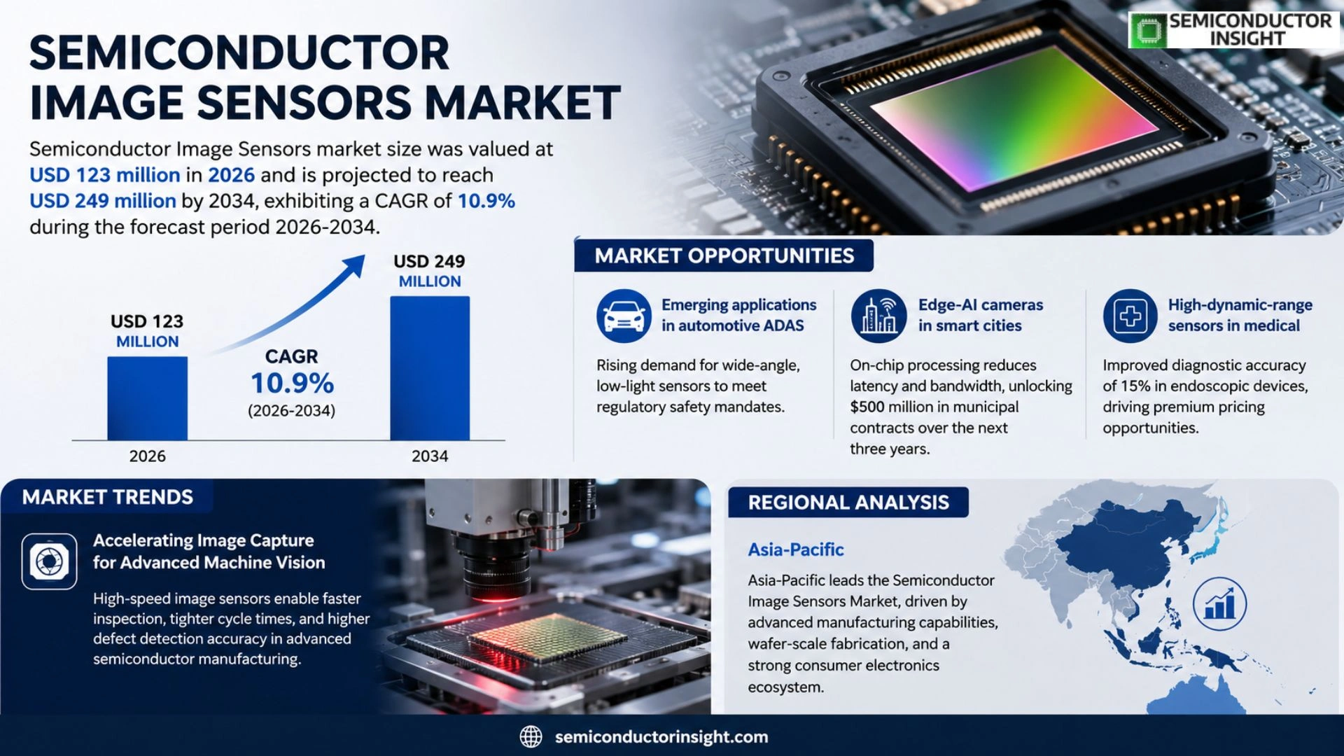
Semiconductor Image Sensors market size was valued at USD 123 million in 2026 and is projected to reach USD 249 million by 2034, exhibiting a CAGR of 10.9% during the forecast period.
Semiconductor image sensors are photodetector devices that convert light into electrical signals, enabling machine‑vision systems, automotive cameras, and consumer electronics to capture high‑resolution images quickly. The two dominant technologies are CCD (charge‑coupled device) and CMOS (complementary metal‑oxide‑semiconductor), each offering distinct trade‑offs in power consumption, speed, and integration flexibility.
The market gains momentum because manufacturers seek faster inspection cycles on production lines; higher sensor performance directly reduces bottlenecks in defect scanning and positioning applications. Simultaneously, expanding IoT deployments push demand for compact CMOS modules that can operate under tight power budgets. Leading players such as Sony, Teledyne, and LMI Technologies continue investing in next‑generation pixel architectures and on‑chip processing capabilities to stay ahead of these requirements.
MARKET DRIVERS
Rising demand for high‑resolution imaging
Smartphone manufacturers are integrating 48‑megapixel sensors to differentiate flagship models, prompting a surge in volume orders for the Semiconductor Image Sensors Market. The premium segment now accounts for roughly 35 % of total shipments, a shift that forces OEMs to prioritize sensor performance over cost. This transition fuels investment in back‑end processes that can sustain finer pixel pitches without sacrificing yield.
Advancements in AI‑enabled vision systems
Industrial automation plants are retrofitting assembly lines with AI‑driven visual inspection cells. Sensors capable of delivering >60 fps at low illumination enable defect detection that was previously impossible. Companies that embed on‑chip neural accelerators see a 12 % reduction in system‑level power consumption, making the technology attractive for edge deployments.
➤ “The convergence of sensor mini‑scaling and on‑chip AI is reshaping the economics of machine vision,” notes a senior analyst at a leading research firm.
These forces converge to create a virtuous cycle: higher resolution drives AI adoption, which in turn justifies further investment in sensor fabrication capacity, strengthening the overall Semiconductor Image Sensors Market trajectory.
MARKET CHALLENGES
Manufacturing yield constraints
As pixel sizes shrink below 1 µm, defect density on silicon wafers becomes a critical bottleneck. Foundries report a 5‑8 % drop in usable die per wafer when moving from 1.1 µm to 0.9 µm processes, inflating unit costs and compressing margins for sensor suppliers.
Other Challenges
Supply‑chain volatility
Geopolitical tensions have limited access to high‑purity silicon substrates, prompting many firms to diversify their supplier base. The resulting lead‑time extensions of 3‑4 weeks can disrupt product launch calendars for automotive OEMs.
MARKET RESTRAINTS
Cost pressure from competing technologies
CMOS sensors now compete with emerging organic photodetectors that promise lower material costs for niche applications such as flexible wearables. While performance still lags, the 10 % price advantage forces price‑sensitive OEMs to evaluate mixed‑technology strategies.
In addition, the expense of transitioning to next‑generation lithography tools can exceed $1 billion per fab, a hurdle that deters smaller players from expanding capacity and concentrates market power among a few incumbents.
Regulatory scrutiny over data privacy, especially in surveillance deployments, imposes additional design constraints that can increase bill‑of‑materials (BOM) and delay time‑to‑market.
MARKET OPPORTUNITIES
Emerging applications in automotive ADAS
Advanced driver‑assistance systems (ADAS) now require wide‑angle, low‑light sensors capable of detecting pedestrians at distances beyond 150 m. The Semiconductor Image Sensors Market is witnessing a 20 % year‑over‑year increase in orders from Tier‑1 automotive suppliers, driven by regulatory mandates for higher safety standards.
Another growth vector stems from edge‑AI cameras used in smart cities. Integrating on‑chip processing reduces latency and bandwidth costs, creating a compelling value proposition for municipal contracts valued at $500 million collectively over the next three years.
Finally, the medical imaging segment is exploring high‑dynamic‑range sensors for endoscopic devices. Early adopters report a 15 % improvement in diagnostic accuracy, positioning sensor manufacturers to capture a premium niche that commands higher margins.
Semiconductor Image Sensors Market Trends
Accelerating Image Capture for Advanced Machine Vision
The rise of high‑speed production lines has forced equipment makers to look beyond traditional optics. Faster image acquisition translates directly into tighter cycle times, allowing factories to push throughput without sacrificing defect detection accuracy. As manufacturers introduce tighter tolerances in semiconductor back‑end processes, the demand for image sensors that can operate at higher frame rates while maintaining low noise levels has become a decisive factor in equipment selection. Suppliers that can deliver sub‑microsecond exposure times are seeing deeper penetration into wafer‑inspection tools, where every missed particle can cost millions.
Other Trends
Quality Assurance Pressures
Stringent quality requirements are reshaping the sensor validation workflow. Each lithography step now incorporates inline inspection stations, and the data generated must be processed in real time to trigger corrective actions. This environment pushes sensor manufacturers to embed on‑chip processing capabilities, reducing latency between capture and analysis. The move toward integrated analytics not only shortens feedback loops but also opens new revenue streams for vendors offering software‑defined sensor solutions.
Edge‑AI Integration Expands Application Reach
Beyond the factory floor, the proliferation of edge AI devices is expanding the addressable market for semiconductor image sensors. Compact, power‑efficient CMOS arrays are being embedded in autonomous robots, smart cameras, and IoT gateways that require real‑time visual inference. The convergence of AI accelerators with sensor front‑ends eliminates the need for bulky host processors, enabling truly distributed vision systems. Companies that align their sensor roadmaps with emerging AI frameworks are positioning themselves to capture growth in sectors such as logistics automation, precision agriculture, and wearable health monitors.
COMPETITIVE LANDSCAPE
Key Industry Players
Semiconductor Image Sensors Market – Competitive Overview
At the apex of the semiconductor image sensor arena, Sony continues to dominate through its extensive CMOS portfolio, which blends high‑resolution performance with robust low‑light capability. The company’s aggressive investment in stacked‑sensor architecture supplies automotive advanced driver‑assistance systems (ADAS) and premium mobile devices, reinforcing its position as a technology leader. Samsung Electronics follows closely, leveraging its massive wafer capacity to push pixel‑size reduction and integrated AI‑on‑chip functions, thereby challenging Sony’s market share in both consumer and industrial segments. The overall market structure is characterized by a small cohort of vertically integrated manufacturers that control design, fabrication, and packaging, while a broader set of fab‑less firms rely on foundry services to compete on niche applications such as medical imaging or high‑speed defect inspection. Recent consolidation,exemplified by ON Semiconductor’s acquisition of Fairchild Imaging,has sharpened competitive pressures, prompting incumbents to deepen collaborations with foundries and to accelerate roadmap timelines.
Beyond the titans, a diverse group of specialized players fuels innovation in targeted verticals. OmniVision Technologies exploits its expertise in low‑power sensors for IoT‑enabled cameras, while Himax focuses on automotive mirror‑less solutions that require extreme durability. Canon and Panasonic preserve relevance by adapting legacy CCD know‑how to hybrid CMOS‑CCD hybrids for precision manufacturing inspection. STMicroelectronics and Sharp pursue strategic partnerships to embed image sensors within broader system‑on‑chip offerings, catering to smart‑home and wearable markets. Gpixel and Pixelplus target the high‑speed wire‑bonding niche, delivering sub‑micron pixel pitches that enable next‑generation semiconductor packaging verification. This constellation of firms, though smaller in revenue, creates a vibrant ecosystem that pushes the envelope on sensor miniaturization, speed, and integration, generating multiple pathways for end‑users to achieve differentiated performance.
List of Key Semiconductor Image Sensors Companies Profiled
- Sony
- Samsung Electronics
- OmniVision Technologies
- Himax
- Canon Inc.
- Panasonic Corporation
- STMicroelectronics
- ON Semiconductor
- Sharp Corporation
- Gpixel
- Pixelplus
- Toshiba
Segment Analysis:
| Segment Category | Sub-Segments | Key Insights |
| By Type |
|
Leading Segment
|
| By Application |
|
Leading Segment
|
| By End User |
|
Leading Segment
|
Regional Analysis: Semiconductor Image Sensors Market
Asia‑Pacific
Manufacturers are re‑configuring logistics networks to mitigate disruptions, placing critical component inventories closer to assembly plants. This shift enables quicker adaptation to demand spikes and reduces exposure to geopolitical bottlenecks, a factor that directly influences pricing power in the sensor segment.
The region’s OEMs are integrating multi‑spectral and high‑resolution sensors into flagship products at a speed that outstrips other markets. Their willingness to embed cutting‑edge capabilities drives sensor vendors to accelerate roadmap execution and prioritize feature differentiation.
Emerging safety standards for automotive vision systems are prompting regional authorities to endorse advanced imaging modules. Companies that anticipate these directives can capture early market share by aligning product certifications with upcoming compliance timelines.
Universities and research institutes in the area generate a steady pipeline of photonics and AI specialists. This talent pool fuels innovation cycles, allowing sensor firms to experiment with novel pixel designs and on‑chip processing without lengthy recruitment lags.
North America
In North America, the Semiconductor Image Sensors Market is shaped by a strong emphasis on premium applications, particularly in autonomous vehicle prototypes and high‑end consumer devices. Companies here focus on integrating AI‑enabled image processing directly onto the sensor die, a strategy that addresses privacy concerns and latency requirements of edge computing. Collaborative ventures between chip designers and software firms create ecosystems where sensor output can be directly consumed by machine‑learning pipelines, offering a competitive advantage for firms that can deliver tightly coupled hardware‑software solutions.
Europe
European stakeholders prioritize compliance and sustainability, influencing sensor development pathways. Stringent environmental directives compel manufacturers to adopt low‑power pixel architectures and recyclable packaging. Furthermore, the region’s automotive sector, renowned for safety‑critical systems, demands sensors with exceptional reliability under varied climatic conditions. This requirement spurs investment in robust testing regimes and reinforces the market’s tilt toward high‑quality, durable imaging solutions.
South America
Growth in South America is anchored by expanding mobile broadband penetration and a nascent interest in smart agricultural technologies. Sensor providers are customizing solutions for low‑cost diagnostic equipment that can operate in remote fields, capitalizing on the region’s need for cost‑effective imaging. The gradual rollout of 5G also opens opportunities for real‑time video analytics, prompting local distributors to explore partnerships that bring advanced sensor modules to emerging applications.
Middle East & Africa
In the Middle East & Africa, the market narrative revolves around infrastructure projects and surveillance requirements. Governments are upgrading security networks with high‑resolution imaging that can feed analytic platforms for crowd management and border monitoring. Meanwhile, oil‑and‑gas operators are trialing rugged sensors for equipment inspection, a use case that emphasizes durability over ultra‑high resolution. These divergent needs encourage a mix of premium and ruggedized sensor offerings within the regional portfolio.
Report Scope
This market research report provides a comprehensive analysis of the Semiconductor Image Sensors Market , covering the forecast period 2026–2034. It offers detailed insights into market dynamics, technological advancements, competitive landscape, and key trends shaping the industry.
Key focus areas of the report include:
- Market Overview: The report begins with an overview outlining its current market scenario, key growth indicators, and industry transformation drivers. It discusses macroeconomic factors, demand–supply balance, regulatory landscape, and the strategic role of semiconductors in powering advancements across industries such as automotive, telecommunications, consumer electronics, and industrial automation.
- Market Size & Forecast: Historical data and future projections for revenue, unit shipments, and market value across major regions and segments.
- Segmentation Analysis: Detailed breakdown by product type, technology, application, and end-user industry to identify high-growth segments and investment opportunities.
- Regional Insights: Insights into market performance across North America, Europe, Asia-Pacific, Latin America, and the Middle East & Africa, including country-level analysis where relevant.
- Competitive Landscape: Profiles of leading market participants, including their product offerings, R&D focus, manufacturing capacity, pricing strategies, and recent developments such as mergers, acquisitions, and partnerships.
- Technology Trends & Innovation: Assessment of emerging technologies, integration of AI/IoT, semiconductor design trends, fabrication techniques, and evolving industry standards.
- Market Drivers & Restraints: Evaluation of factors driving market growth along with challenges, supply chain constraints, regulatory issues, and market-entry barriers.
- Stakeholder Insights: Insights for component suppliers, OEMs, system integrators, investors, and policymakers regarding the evolving ecosystem and strategic opportunities.
Primary and secondary research methods are employed, including interviews with industry experts, data from verified sources, and real-time market intelligence to ensure the accuracy and reliability of the insights presented.
FREQUENTLY ASKED QUESTIONS:
What is the current market size of Semiconductor Image Sensors Market?
-> Semiconductor Image Sensors market is projected to reach USD 249 million by 2034, exhibiting a CAGR of 10.9% during the forecast period.
Which key companies operate in Semiconductor Image Sensors Market?
-> Key players include Sony, Teledyne, LMI Technologies, among others.
What are the key growth drivers?
-> Key growth drivers include increasing demand for faster image scanning in machine‑vision applications, tighter quality‑control requirements, and the push for higher‑performance CMOS sensors to support advanced automation and IoT devices.
Which region dominates the market?
-> Asia leads the market, driven by large semiconductor manufacturing bases in China, Japan, and South Korea.
What are the emerging trends?
-> Emerging trends include integration of AI/IoT for smart vision, development of high‑resolution CMOS sensors, and adoption of miniaturized sensor packages for compact devices.

Get Sample Report PDF for Exclusive Insights
Report Sample Includes
- Table of Contents
- List of Tables & Figures
- Charts, Research Methodology, and more...
 Download Sample Report PDF