Semiconductor Etching Equipment Market Insights
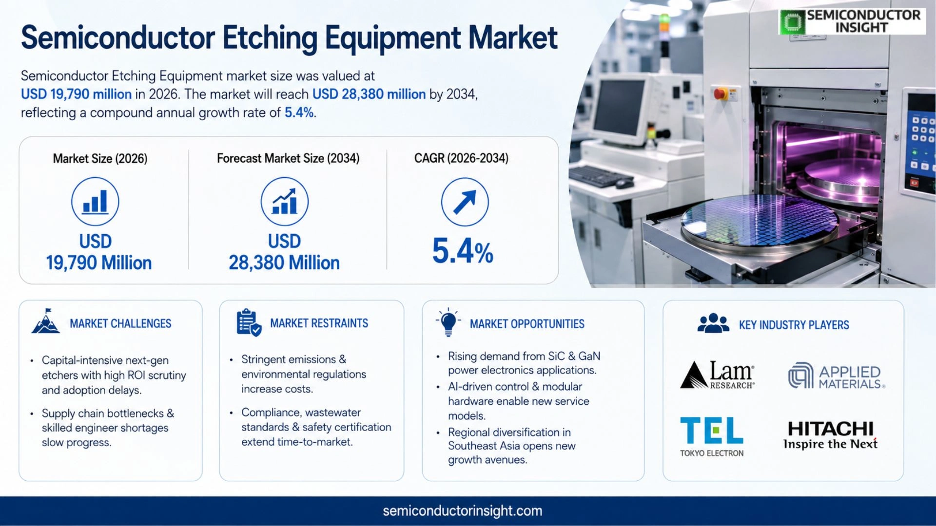
Semiconductor Etching Equipment market size was valued at USD 19,790 million in 2026. The market will reach USD 28,380 million by 2034, reflecting a compound annual growth rate of 5.4 percent over the period.
Etching removes material from wafer surfaces using chemicals; an etch system shapes thin films into desired patterns through liquid chemicals, reactive gases or ion reactions. Semiconductor etch equipment,both dry and wet technologies,is integral to every stage of semiconductor fabrication.
The expansion stems from increasing demand for high‑performance computing platforms, AI‑enabled servers and advanced logic‑memory nodes. While dry‑etch tools continue to hold the largest revenue share because of precision control, wet‑etch solutions are gaining ground thanks to higher removal rates and simpler operation.
MARKET DRIVERS
Advanced Node Scaling Demands
Semiconductor Etching Equipment market is being pulled forward by manufacturers racing to embed sub‑10 nm features into logic chips. As design rules tighten, etch tools must deliver sub‑nanometer uniformity while preserving high throughput. This pressure forces equipment vendors to embed real‑time plasma analytics, turning process windows into competitive differentiators.
Materials Innovation and Process Complexity
Emerging high‑k dielectrics, metal‑gate stacks and three‑dimensional architectures demand etch chemistries that can discriminate between ultrathin layers without causing damage. Vendors that succeed in coupling low‑damage fluorine‑based chemistries with advanced endpoint detection gain immediate market traction, as fabs look to reduce cycle time penalties associated with multi‑step processes.
➤ Customers are shifting spend from incremental upgrades to breakthrough etch platforms that enable new transistor topologies.
These dynamics compel OEMs to expand R&D budgets and accelerate product rollouts, creating a virtuous loop where higher‑performance tools unlock the next generation of chips, which in turn fuels further equipment investment.
MARKET CHALLENGES
Capital Intensity of New Platforms
Deploying next‑generation etchers requires multi‑hundred‑million‑dollar outlays per fab line. Financial committees scrutinize ROI projections closely, often opting for phased upgrades rather than wholesale replacement, which can elongate adoption cycles.
Moreover, the steep learning curve associated with novel plasma chemistries introduces yield risk during early production runs. Managers must balance the allure of cutting‑edge capability against the reality of potential throughput dips.
Other Challenges
Supply Chain Bottlenecks
Limited availability of high‑purity precursor gases and specialized vacuum components creates scheduling friction, especially when geopolitical factors constrain cross‑border logistics.
In parallel, the scarcity of skilled etch engineers amplifies the challenge, as talent pipelines struggle to keep pace with the rapid evolution of tool architectures.
MARKET RESTRAINTS
Regulatory and Environmental Compliance
Stringent emissions regulations governing fluorinated gases impose additional cost layers on equipment manufacturers, who must integrate abatement systems without sacrificing process speed. This compliance burden can erode margin potential for smaller players.
Beyond chemicals, waste‑water discharge standards force fabs to invest in on‑site treatment facilities, further inflating the total cost of ownership for advanced etch platforms.
The need to certify equipment against evolving safety standards also elongates time‑to‑market, as each new generation must undergo extensive validation cycles before deployment.
MARKET OPPORTUNITIES
Emerging Applications in Power Electronics
Growth in silicon‑carbide and gallium‑nitride power devices is driving demand for etching solutions that can sculpt high‑aspect‑ratio structures with minimal defectivity. Suppliers that tailor plasma profiles for wide‑bandgap substrates stand to capture a fast‑moving niche.
Additionally, the convergence of artificial‑intelligence‑driven process control with modular hardware designs opens pathways for fab‑as‑a‑service models. Companies that bundle predictive maintenance analytics with equipment leasing can unlock recurring revenue streams while lowering entry thresholds for midsize fabs.
Finally, regional diversification initiatives,particularly in Southeast Asia,are prompting local fabs to source equipment that balances performance with cost‑effective support structures, presenting a clear growth corridor for vendors willing to establish on‑ground service networks.
Semiconductor Etching Equipment Market Trends
Shift Toward Wet Etching for High‑Throughput Nodes
The wet etching segment is seeing increased adoption as manufacturers target throughput improvements for logic and memory nodes below 10 nm. By leveraging liquid‑phase chemistries, fabs can achieve etch rates that surpass many dry‑processes while maintaining pattern fidelity, a combination that reduces cycle time on 300‑mm wafers. Recent equipment releases incorporate in‑situ gas recycling, cutting consumable costs and easing environmental compliance. Because many emerging applications,such as power‑device thinning and MEMS resonators,require high material removal without plasma‑induced damage, suppliers are prioritizing wet‑tool portfolios. This shift reshapes Semiconductor Etching Equipment market, prompting original equipment manufacturers to allocate engineering resources toward modular wet stations that can be retrofitted onto existing lines. Furthermore, the cost advantage of fewer plasma chambers translates into lower capital expenditure for mid‑tier fabs, accelerating adoption in emerging markets. These dynamics also create opportunities for service providers offering predictive maintenance based on wet‑process data.
Other Trends
Regional Realignment Driven by Capacity Expansion
Asia–Pacific continues to dominate the back‑end landscape, yet a noticeable reallocation of capacity is unfolding across the region. Mainland China and South Korea together account for well over half of the installed base, but recent policy incentives in Taiwan and Japan have accelerated the commissioning of new wet and dry etch lines aimed at 5‑nm and sub‑5‑nm products. In North America, a cluster of advanced‑logic fabs is expanding its dry‑etch inventory to support heterogeneous integration of photonic and silicon‑carbon components. European players are focusing on niche markets such as RF‑ID and image‑sensor etching, where precision outweighs volume. These geographic adjustments translate into altered supply‑chain dynamics, with component manufacturers adjusting lead‑times to match the divergent demand profiles across regions. Supply‑chain firms are accordingly diversifying their inventory of photo‑resists and specialty gases to service both wet and dry lines, reducing exposure to single‑source constraints.
Emergence of Advanced Dry‑Plasma Solutions for 3‑nm and Beyond
Parallel to the wet‑etch movement, the industry is investing heavily in next‑generation dry‑plasma platforms capable of atomic‑scale control. Suppliers are integrating high‑density inductively coupled plasma sources with real‑time endpoint detection, enabling feature sizes that approach 3 nm without compromising uniformity across 300‑mm substrates. The introduction of low‑damage chemistries, such as fluorocarbon‑free gas mixes, addresses reliability concerns for emerging three‑dimensional architectures. Capital commitments from leading fabs signal that these advanced dry tools will become standard for high‑performance computing and AI accelerators, where device density and power efficiency are paramount. The convergence of dry‑plasma capability with AI‑driven process optimization further shortens cycle time, allowing fabs to ramp new node volumes within tighter investment windows. As a result, the equipment ecosystem is witnessing a convergence of process engineering and software analytics, reshaping product roadmaps and competitive positioning.
COMPETITIVE LANDSCAPE
Key Industry Players
Semiconductor Etching Equipment Market: Competitive Overview 2024‑2031
In 2024 the etching segment remains dominated by a handful of multinational OEMs whose portfolios span both dry and wet systems. Lam Research retains the top‑revenue position thanks to its aggressive line‑extension in high‑aspect‑ratio trench etch tools, which are indispensable for logic and memory nodes below 5 nm. Applied Materials leverages its broad wafer‑fab customer base, integrating plasma‑enhanced processes that reduce cycle time, thereby cementing its foothold in both legacy and leading‑edge fabs. Tokyo Electron continues to extract market share by bundling its etch platforms with advanced metrology solutions, a strategy that appeals to customers seeking end‑to‑end process control. The concentration of revenue among these three firms forces smaller vendors to specialize, either by focusing on niche processes such as dielectric etch for MEMS or by offering cost‑effective wet‑etch stations for emerging foundries. This oligopolistic structure intensifies pricing pressure on downstream manufacturers, prompting them to negotiate multi‑year service contracts that embed technology refresh cycles.
Beyond the tier‑one trio, a diverse set of specialists shapes the competitive landscape. Hitachi High‑Tech and SEMES have carved out leadership in high‑precision plasma etch tools for display and sensor applications, where line‑edge definition is critical. Advanced Micro and NAURA target the mid‑volume market, supplying modular wet‑etch reactors that lower entry barriers for regional fabs in China and Southeast Asia. ULVAC and SPTS Technologies differentiate themselves through proprietary RF‑source technologies that improve etch uniformity for thin‑film deposition lines. Plasma‑Therm’s focus on high‑density inductively coupled plasma (ICP) equipment caters to power‑device manufacturers confronting stringent leakage requirements. GigaLane and Oxford Instruments sustain niche relevance by providing customizable solutions for R&D labs and low‑volume production of RF‑ICs and quantum‑chip prototypes. Beijing E‑Town, though less visible internationally, benefits from strong domestic policy support, enabling it to capture a share of the rapidly expanding Chinese fab ecosystem. Collectively, these players generate a competitive pressure that accelerates innovation cycles, as each seeks to differentiate through throughput, pattern fidelity, and total cost of ownership.
List of Key Semiconductor Etching Equipment Companies Profiled
- Lam Research
- Applied Materials
- Tokyo Electron (TEL)
- Hitachi High‑Tech
- SEMES
- Advanced Micro
- NAURA
- ULVAC
- SPTS Technologies
- Plasma‑Therm
- GigaLane
- Oxford Instruments
- Beijing E‑Town
Segment Analysis:
| Segment Category | Sub-Segments | Key Insights |
| By Type |
|
Dry Etching Equipment
|
| By Application |
|
Logic and Memory
|
| By End User |
|
Foundries
|
| By Film Type |
|
Dielectric Etching
|
| By Process Trend |
|
Atomic Layer Etching (ALE)
|
Regional Analysis: Semiconductor Etching Equipment Market
Asia‑Pacific
Localized component sourcing and the establishment of regional logistics hubs have shortened the procurement cycle for etching modules. Vendors are integrating buffer inventories and dual‑sourcing strategies, which cushions the market against global disruptions and stabilizes pricing for end‑users.
Foundries are allocating a larger share of capex to next‑generation etch equipment that can handle high‑aspect‑ratio structures. This capital focus nudges equipment makers to prioritize R&D in plasma uniformity and endpoint detection, reinforcing a feedback loop of innovation.
National semiconductor roadmaps across the region explicitly earmark funds for advanced lithography and etch solutions. Policy continuity reduces fiscal risk for equipment providers and encourages long‑term partnership agreements.
A surge in demand for AI accelerators and automotive processors drives fabs to adopt finer etch techniques. Equipment vendors that can deliver rapid tooling upgrades capture a larger share of the aftermarket service revenue.
North America
North America remains a mature arena where Semiconductor Etching Equipment market is characterized by high adoption of precision etching for mature and leading‑edge nodes alike. The region’s established ecosystem of design houses and integrated device manufacturers creates a steady cadence for equipment refresh cycles. However, the market’s elasticity is tempered by stringent environmental regulations that influence gas usage and waste management, prompting vendors to introduce greener process chemistries. Partnerships between equipment firms and major fabs often extend beyond purchase orders into joint development programs, which align product roadmaps with customer process challenges. For operators, this translates into reduced downtime and a more predictable cost structure for equipment depreciation.
Europe
Europe’s semiconductor sector, anchored by a network of specialty fabs and research institutions, contributes nuanced pressure on Semiconductor Etching Equipment market. The continent’s emphasis on sustainability has led to increased scrutiny of process gases and energy consumption, motivating equipment makers to embed efficiency metrics within their platforms. At the same time, the EU’s strategic initiatives to bolster domestic chip production generate new opportunities for localized equipment supply chains. Manufacturers that can demonstrate compliance with European standards while delivering high‑throughput etch solutions are gaining preferential access to emerging contracts. The overall effect is a market that rewards both technological excellence and regulatory agility.
South America
South America’s role in Semiconductor Etching Equipment market is evolving from peripheral support to a more active participant as regional governments pursue semiconductor diversification strategies. Emerging fabs in Brazil and Chile are seeking cost‑effective etching solutions that balance performance with operational simplicity. Vendors are responding with modular equipment designs that can be scaled according to production volume, reducing upfront capital requirements. Additionally, the region’s growing pool of engineering talent enables collaborative troubleshooting and localized after‑sales support, which enhances equipment uptime and fosters customer loyalty.
Middle East & Africa
The Middle East & Africa region is gradually entering Semiconductor Etching Equipment market narrative, primarily through investment in downstream assembly and testing facilities. While full‑scale wafer fabrication remains limited, the presence of advanced packaging plants creates a niche demand for precise etching of interconnect layers. Equipment suppliers are leveraging this opportunity by offering low‑volume, high‑precision tools that cater to specialty applications. Furthermore, the region’s strategic positioning as a logistics hub facilitates quicker delivery of spare parts and service personnel, improving overall equipment reliability for early adopters.
Report Scope
This market research report provides a comprehensive analysis of the Semiconductor Etching Equipment Market , covering the forecast period 2026–2034. It offers detailed insights into market dynamics, technological advancements, competitive landscape, and key trends shaping the industry.
Key focus areas of the report include:
- Market Overview: The report begins with an overview outlining its current market scenario, key growth indicators, and industry transformation drivers. It discusses macroeconomic factors, demand–supply balance, regulatory landscape, and the strategic role of semiconductors in powering advancements across industries such as automotive, telecommunications, consumer electronics, and industrial automation.
- Market Size & Forecast: Historical data and future projections for revenue, unit shipments, and market value across major regions and segments.
- Segmentation Analysis: Detailed breakdown by product type, technology, application, and end-user industry to identify high-growth segments and investment opportunities.
- Regional Insights: Insights into market performance across North America, Europe, Asia-Pacific, Latin America, and the Middle East & Africa, including country-level analysis where relevant.
- Competitive Landscape: Profiles of leading market participants, including their product offerings, R&D focus, manufacturing capacity, pricing strategies, and recent developments such as mergers, acquisitions, and partnerships.
- Technology Trends & Innovation: Assessment of emerging technologies, integration of AI/IoT, semiconductor design trends, fabrication techniques, and evolving industry standards.
- Market Drivers & Restraints: Evaluation of factors driving market growth along with challenges, supply chain constraints, regulatory issues, and market-entry barriers.
- Stakeholder Insights: Insights for component suppliers, OEMs, system integrators, investors, and policymakers regarding the evolving ecosystem and strategic opportunities.
Primary and secondary research methods are employed, including interviews with industry experts, data from verified sources, and real-time market intelligence to ensure the accuracy and reliability of the insights presented.
FREQUENTLY ASKED QUESTIONS:
What is the current market size of Semiconductor Etching Equipment Market?
-> Semiconductor Etching Equipment market will reach USD 28,380 million by 2034, reflecting a compound annual growth rate of 5.4 percent
Which key companies operate in Semiconductor Etching Equipment Market?
-> Key players include Lam Research, TEL, Applied Materials, Hitachi High-Tech, SEMES, Advanced Micro, KLA, NAURA, ULVAC, SPTS Technologies, Plasma-Therm, GigaLane, Oxford Instruments, Beijing E‑Town, among others.
What are the key growth drivers?
-> Key growth drivers include high‑performance computing, artificial intelligence, cloud computing, servers, 5G deployment, and electric vehicles (EV), all of which drive demand for advanced etching solutions.
Which region dominates the market?
-> Asia dominates the market, with China mainland, Taiwan and South Korea together accounting for over 70% of global semiconductor equipment share.
What are the emerging trends?
-> Emerging trends include the rapid adoption of wet etching equipment due to its higher etching rates and operational ease, as well as increasing focus on “green” etching processes that reduce material consumption and disposal costs.

Get Sample Report PDF for Exclusive Insights
Report Sample Includes
- Table of Contents
- List of Tables & Figures
- Charts, Research Methodology, and more...
 Download Sample Report PDF