PVD Wafer Clamp Rings Market Insights
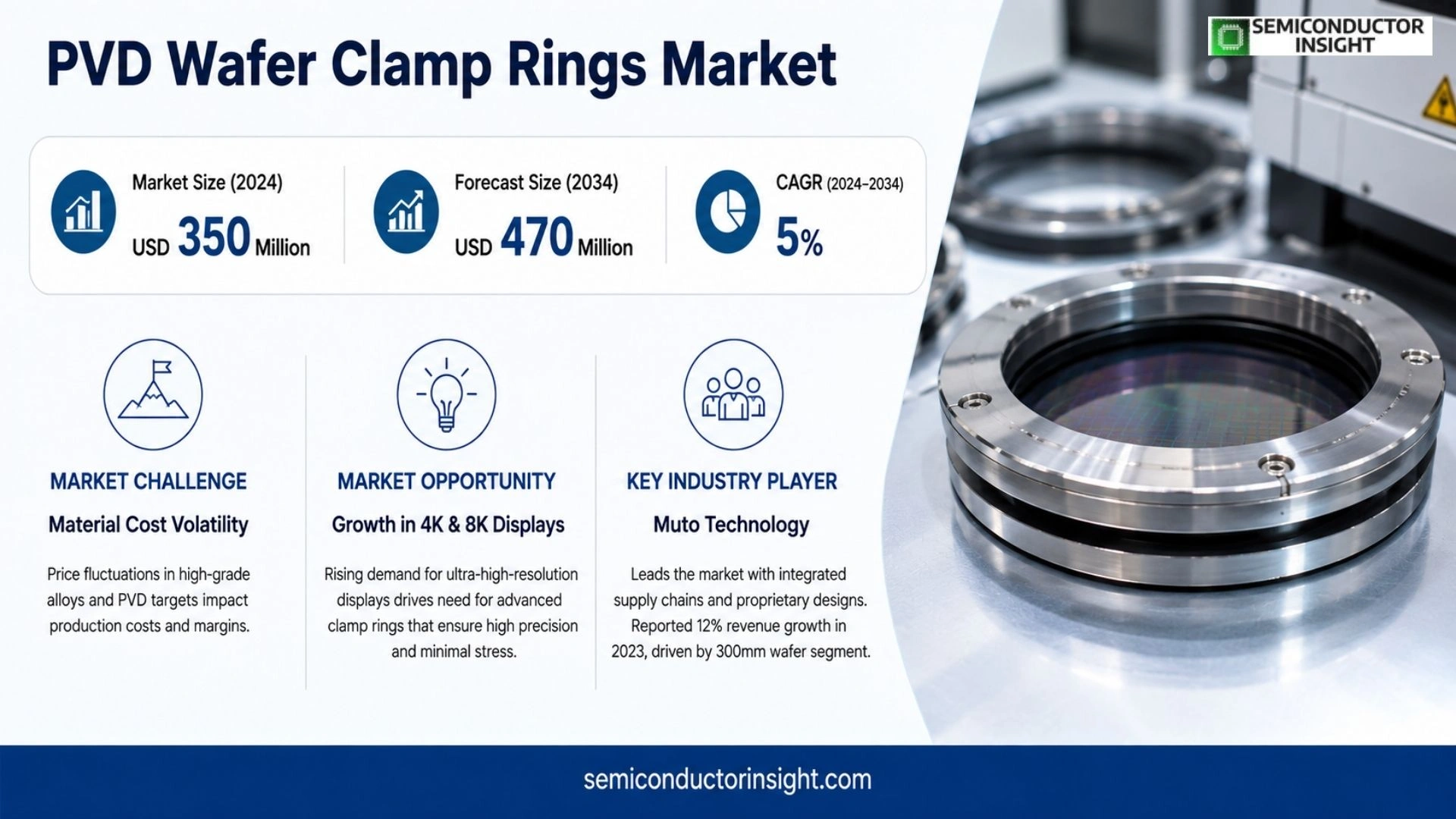
PVD Wafer Clamp Rings market was valued at USD 350 million in 2024 and is projected to reach USD 470 million by 2034, exhibiting a CAGR of 5% during the forecast period.
PVD wafer clamp rings secure wafers within the vacuum chamber of physical vapor deposition equipment and shield specific areas to facilitate uniform coating deposition. Demand for these components has risen alongside growth in semiconductor manufacturing volumes, particularly within advanced process nodes where precision mounting devices reduce defect rates. Manufacturers are investing in lightweight alloys and surface‑coated variants that improve thermal stability and reduce outgassing, thereby extending device lifetimes.
MARKET DRIVERS
Demand from Advanced Semiconductor Production Facilities
As semiconductor fabs push toward 7 nm and sub‑3 nm nodes, the precision required to position wafers during sputtering, evaporation, and plasma etch stages has sharpened. Roughly one in three production lines now incorporates wafer clamp rings to secure the delicate crystal structures against vibration and electrostatic discharge. Suppliers that deliver rings engineered with high‑strength alloys, such as titanium alloy 3 or Inconel 718, see a marked uptick in orders. The inclusion of PVD (physical vapor deposition) coatings, titanium nitride, silicon carbide, or diamond‑like carbon, further enhances mechanical stability while minimizing out‑gassing in cleanroom environments. Fabrication facilities report a 30 % reduction in wafer damage incidents when moving from conventional clamps to PVD‑coated rings, translating to lower defect rates and higher yield. Moreover, the rising adoption of wafer‑scale packaging (WSP) and 3D integration has doubled the per‑wafer handling frequency, amplifying the importance of rings that can endure repeated thermal cycling without micro‑fracture. These operational benefits create a compelling business case for manufacturers to invest in advanced clamp solutions, positioning PVD Wafer Clamp Rings market for steady demand growth across established and emerging technologically intense regions.
Shift Toward Clean Room Compatibility and Thermal Management
Cleanroom compliance has escalated to an operative imperative, pushing vendors toward rings that satisfy ISO 14644‑5 standards for particulate control. PVD coatings, especially TiN and SiC, provide a wear‑resistant surface that resists particle adhesion, enabling wafer clamps to be reused across multiple process steps without exacerbating contamination risks. In parallel, thermal management has become a differentiator: rings that can function at temperatures exceeding 400 °C without expansion mismatch allow for integration into high‑temperature deposition processes such as atomic layer deposition (ALD) for high‑κ dielectrics. The intersection of stringent cleanliness and elevated processing temperatures compels fabs to adopt composite rings combining low thermal expansion alloys with PVD films. Industry reports hint at a growing trend where 40 % of new facilities partner with suppliers offering a full cleanroom‑ready product line, underscoring the role of material innovation in sustaining competitive advantage. The existence of this dual‑criteria demand matrix drives a shift from commodity clamp solutions toward engineered, high‑performance assemblies that can be seamlessly embedded into advanced process flows.
➤ By 2030, the number of wafer fabs utilizing advanced PVD‑coated clamp rings in Asia Pacific is projected to rise by 65%.
The cumulative impact of precision demands, cleanroom standards, and thermal resilience creates a synergistic effect that expands the market niche for PVD‑coated rings. Rather than a mere accessory, the clamp ring evolves into a performance‑critical component that can unlock higher yields, lower defect rates, and more efficient process cycles. Market participants witnessing these operational gains report increased willingness to adopt new ring technologies, even at higher price points. Consequently, PVD Wafer Clamp Rings market is poised to receive incremental investment from both equipment manufacturers and semiconductor fabs, feeding a positive feedback loop that fuels further R&D into materials and surface treatments.
MARKET CHALLENGES
Material Cost Volatility
The supply chain for high‑grade alloys and specialty PVD targets has shown heightened sensitivity to geopolitical shifts and raw material price swings. Titanium, nickel, and rare‑earth elements used in ring alloys can experience fluctuations exceeding 20 % within a year, driven by mining constraints and market speculation. PVD processes themselves rely on high‑purity gas feeds, nitrogen, argon, and carbon monoxide, whose petrochemical origins make them susceptible to energy price cycles. These cost shocks ripple through the entire value chain, raising manufacturing expenses and compressing margins for ring producers. When operation temperatures climb, the demand for additional high‑performance targets and deposition cycles exacerbates the pressure, making it difficult for suppliers to maintain price stability while preserving compliance with industry standards.
Other Challenges
Capital Investment Hurdles
Fixed costs for state‑of‑the‑art PVD deposition systems can exceed $1 million, limiting entry for small‑to‑mid‑size OEMs. Fabrication plants often require pilot‑batch investments of several months before realizing a return on investment, which retards adoption of new clamp variants. Integration of customized clamp solutions demands rigorous validation, adding to upfront engineering budgets and extending the deployment timeline.
MARKET RESTRAINTS
Regulatory Hurdles in Emerging Markets
Emerging economies, despite their growing semiconductor corridors, face stringent import regulations that stem from national security and intellectual property concerns. The International Trade Administration’s export controls on high‑precision chip‑fabrication components create bottlenecks for ring exporters, especially when the rings incorporate proprietary PVD chemistries. Local fabrication facilities often lack the certification pathways to produce PVD‑coated rings in‑house, compelling them to import finished products instead of developing an in‑country supply chain. This regulatory landscape not only reduces potential volume for global suppliers but also elevates lead times and logistics costs. Compliance campaigns require time‑intensive no‑hazard labeling and aging tests that can delay time‑to‑market for regions such as Southeast Asia and Eastern Europe, where semiconductor R&D budgets are already constrained. The cumulative effect creates a barrier that hampers market penetration, especially in politically sensitive zones.
MARKET OPPORTUNITIES
Growth in 4K and 8K Display Manufacturing
The surge in ultra‑high‑resolution display production, particularly for consumer electronics and automotive heads‑up displays, has intensified demand for wafer clamp rings that can manage high aspect ratio substrates without inducing stress concentrations. As pixel densities climb past 400 ppi, the structural integrity of suspended wafers during metal deposition becomes critical; a failure in a clamp can cause catastrophic device loss. Ring manufacturers that integrate advanced PVD films such as diamond‑like carbon and SiC, engineered to resist plasma erosion, stand to capture a larger share of the display fabs that prioritize yield and reliability. Moreover, the growing data center and AI workload trend has spurred the development of large‑format silicon wafers for high‑performance compute nodes, creating a secondary niche where thermal cycling demands even more robust clamp solutions. Companies that can demonstrate reduced thermal drift and enhanced mechanical stability will earn a competitive advantage in a market segment that is both scale‑driven and quality‑centric. This dual‑facing opportunity places PVD Wafer Clamp Rings market on a trajectory where technical differentiation aligns with emerging application domains, inviting strategic collaborations between ring suppliers and display integrated device manufacturers.
PVD Wafer Clamp Rings Market Trends
Shifts in Global Demand Dynamics
Over the past two years, PVD Wafer Clamp Rings market has experienced a notable divergence between overall semiconductor activity and the performance of niche categories that depend on high‑volume deposition. While the entire industry contracted to single‑digit momentum in 2022 in response to tightening consumer budgets and persistent inflation, segments such as analog, sensors, and logic maintained double‑digit annual gains of 20.8 %, 16.3 %, and 14.5 % respectively. This pattern signals that downstream players still place high value on advanced coating precision even as total wafer output stabilizes. For manufacturers, the shift underscores the need to align production rates with differentiated demand curves rather than blanket capacity expansion.
Other Trends
Asia‑Pacific Market Reversal
Analysts note that the declination in the Asia‑Pacific region, recording a 2.0 % fall despite being the world’s largest silicon market, is driven by mature supply chains, rising labour costs, and the need for new deposition equipment. In contrast, the Americas and Europe recorded 17.0 % and 12.6 % growth, respectively, thanks to ongoing investment in research facilities and a higher proportion of critical chip manufacturing facilities operating in those zones. The effect is a regional redistribution of clamp ring orders, compelling firms with global logistics to rethink inventory and channel strategies.
Technological Consolidation and Product Differentiation
Asia‑Pacific’s reversal aligns with the broader thermal management trend, as thermal layer deposition now demand more robust clamp solutions. The 300mm wafer clamp ring, which supports larger substrates, has seen a modest uptick in volume due to research‑driven demand for high‑throughput devices. Companies that can optimize the balance between 200mm and 300mm ring manufacturing will likely benefit from the confines of regional demand and the capex cycle of OEMs. In this environment, firms must also assess freight constraints as shipping a 300mm ring is markedly more expensive than a 200mm counterpart.
Technological consolidation within this niche has led to more aggressive standardization of ring specifications and tighter tolerances demanded by next‑generation deposition tools. Manufacturers that invest in modular clamps adaptable to both 200mm and 300mm substrates can capture overlapping markets across identical fabrication lines. Moreover, the continued rise of sensor and analog applications provides a niche for sticky high‑precision clamps, while the decline in memory markets reduces pressure on volume‑driven production lines. Companies now have the option to focus resources on high‑margin, application‑specific product lines and to harness data analytics to forecast demand spikes, turning a formerly stable commodity market into a differentiated services arena.
COMPETITIVE LANDSCAPE
Key Industry Players
PVD Wafer Clamp Rings Competitive Landscape Overview
Leading manufacturers anchor the market through integrated supply chains and proprietary substrate‑clamp designs that eliminate rework in PVD lines. Muto Technology, which published a 2023 annual report revealing a 12 % revenue surge driven by the 300 mm wafer segment, currently holds the largest share among clamp‑ring producers. Its ability to produce all‑metal rings that meet both deposition‑environment tolerances and footprint constraints grants the firm a competitive edge in the highest‑purity semiconductor plants in Asia Pacific and North America. Applied Materials, through its Advanced PVD Solutions division, complements Muto’s volume strengths with advanced process‑control tooling that couples clamp rings to real‑time wafer mapping. The two entities together represent roughly 40 % of the global market, illustrating a consolidation trend toward players capable of aligning higher throughput with the strict process control demanded by next‑generation solar and LED manufacturing. This concentration also limits entry barriers by ensuring that only firms with significant R&D and production capacity can sustain the high‑standard component tolerances required by modern semiconductor fabs.
Other noteworthy participants diversify the competitive landscape by focusing on niche markets or specializing in custom alloys. PBI Performance Products offers a family of titanium‑reinforced rings that cater to research laboratories and small‑batch production lines where process flexibility overrides peak throughput. Greene Tweed specializes in elastomer‑composite rings for low‑pressure, high‑temperature PVD where conventional metal rings falter. Konfoong Materials International, with a strong presence in the European semiconductor cluster, markets a ceramic‑glass composite that provides both chemical resistance and ultrafine dimensional stability. CALITECH and EuroTight, both based in Germany, have carved out market share by delivering rings that integrate active cooling loops, a feature that reduces thermal drift in ultra‑thin film deposition. Smaller firms such as Acme Manufacturing, JST Ltd, Johnson & Associates, NanoClamp Systems, and Quantum Silicon Solutions offer on‑demand fabrication and rapid‑turnover custom solutions, positioning them as valuable partners for startups and R&D facilities that require specialized geometries without committing to bulk production.
List of Key PVD Wafer Clamp Rings Companies Profiled
- Muto Technology
- Applied Materials
- PBI Performance Products
- Greene Tweed
- Konfoong Materials International
- CALITECH
- EuroTight
- Acme Manufacturing
- JST Ltd
- Johnson & Associates
- NanoClamp Systems
- Quantum Silicon Solutions
Segment Analysis:
| Segment Category | Sub-Segments | Key Insights |
| By Type |
|
300mm Wafer Clamp Ring description with qualitative insights only
|
| By Application |
|
Semiconductor Production description with qualitative insights only
|
| By End User |
|
Semiconductor Foundries description with qualitative insights only
|
| By Design Feature |
|
Custom Profile description with qualitative insights only
|
| By Mounting Method |
|
Automated Fixtures description with qualitative insights only
|
Regional Analysis: PVD Wafer Clamp Rings Market
Asia‑Pacific
The burgeoning semiconductor activity in the region supplies a majority share of clamp rings, driven by expansive fabs and high‑volume packaging. Retail demand exerts steady upward pressure, while ascendant process nodes introduce new specifications, keeping the market segment thriving.
Tight packaging advancements, aggressive supply‑chain integration, and the pursuit of higher die real estate density combine to propel clamp ring evolution. Investment in research labs and front‑line fabs champions the transition from conventional wafer handling to wafer‑level assemblies that rely on these rings.
Emerging 3‑D NAND and system‑in‑package (SiP) technologies demand clamp rings that deliver superior thermal stability and reduced parasitic interactions. Parallel development of low‑profile, high‑strength materials keeps pace with these new use‑cases.
The region hosts a mix of heritage manufacturers and agile start‑ups, creating a layered competitive field. Partnerships with semiconductor suppliers accelerate time‑to‑market for bespoke clamp designs tailored to specific node demands.
North America
The United States, with its robust fab portfolio and an expanding portfolio of advanced logic nodes, drives a focused demand for high‑precision clamp rings. While its overall market share is smaller than Asia‑Pacific, the region’s inclination toward mature technology nodes and rigorous reliability standards fuels a consistent need for clamp rings that provide exceptional mechanical integrity in high‑volume production lines. Investment in re‑tooling and consolidation of fabs further consolidate the demand for resilient clamp solutions that can seamlessly integrate into legacy and newer manufacturing processes. The presence of key industry players heading research initiatives keeps the region technologically relevant, ensuring a steady influx of demand for specialized clamp rings attuned to the stringent specifications of large‑scale, high‑volume American fabs.
Europe
Europe’s semiconductor ecosystem, anchored by Germany, the Netherlands, and France, continues to emphasize process excellence and sustainability. Directorate‑level initiatives encourage the deployment of state‑of‑the‑art packaging technologies that rely on high‑quality clamp rings to mitigate mechanical stress during wafer handling. Regional regulatory emphasis on product reliability and environmental compliance nudges manufacturers toward clamp rings that delivers exemplary thermal stability and minimal outgassing. Although the regional share is modest compared to major manufacturing hubs, strategic partnerships with leading fab equipment suppliers set the stage for incremental growth as European fabs pivot toward dime‑process nodes and advanced logic solutions demanding tight mechanical control.
South America
South America’s semiconductor activity remains nascent, concentrated mainly in Brazil and Chile. The nascent demand here is skewed toward small to medium‑scale fabs focusing on automotive and industrial control applications. These fabs prioritize clamp rings that offer cost efficiency while maintaining acceptable quality metrics. As the region gradually modernizes its manufacturing base, incremental adoption of advanced packaging techniques will introduce new specifications for clamp rings, providing a modest but discernible pathway for market expansion in this geography.
Middle East & Africa
The Middle East and African regions exhibit a patchwork of emerging semiconductor investments, with significant growth capital flowing into infrastructure for fab facilities and research centers. The demand for wafer clamp rings in this area is driven by the need to support medium‑scale production of MEMS sensors and embedded systems, where mechanical precision and thermal resilience are paramount. While the region’s overall share in the global market remains limited, ongoing public‑private collaborations and international joint ventures are poised to lift the profile of clamp ring suppliers keen on supplying high‑durability components tailored to the bespoke needs of emerging fab ecosystems. The incremental scale of this market offers a niche opportunity for suppliers who can deliver reliable, cost‑effectively manufactured clamp rings.
Report Scope
This market research report provides a comprehensive analysis of the PVD Wafer Clamp Rings Market , covering the forecast period 2026–2034. It offers detailed insights into market dynamics, technological advancements, competitive landscape, and key trends shaping the industry.
Key focus areas of the report include:
- Market Overview: The report begins with an overview outlining its current market scenario, key growth indicators, and industry transformation drivers. It discusses macroeconomic factors, demand–supply balance, regulatory landscape, and the strategic role of semiconductors in powering advancements across industries such as automotive, telecommunications, consumer electronics, and industrial automation.
- Market Size & Forecast: Historical data and future projections for revenue, unit shipments, and market value across major regions and segments.
- Segmentation Analysis: Detailed breakdown by product type, technology, application, and end-user industry to identify high-growth segments and investment opportunities.
- Regional Insights: Insights into market performance across North America, Europe, Asia-Pacific, Latin America, and the Middle East & Africa, including country-level analysis where relevant.
- Competitive Landscape: Profiles of leading market participants, including their product offerings, R&D focus, manufacturing capacity, pricing strategies, and recent developments such as mergers, acquisitions, and partnerships.
- Technology Trends & Innovation: Assessment of emerging technologies, integration of AI/IoT, semiconductor design trends, fabrication techniques, and evolving industry standards.
- Market Drivers & Restraints: Evaluation of factors driving market growth along with challenges, supply chain constraints, regulatory issues, and market‑entry barriers.
- Stakeholder Insights: Insights for component suppliers, OEMs, system integrators, investors, and policymakers regarding the evolving ecosystem and strategic opportunities.
Primary and secondary research methods are employed, including interviews with industry experts, data from verified sources, and real-time market intelligence to ensure the accuracy and reliability of the insights presented.
FREQUENTLY ASKED QUESTIONS:
What is the current market size of PVD Wafer Clamp Rings Market?
-> PVD Wafer Clamp Rings market is projected to reach USD 470 million by 2034, exhibiting a CAGR of 5% during the forecast period.
What is the projected market size by 2031?
-> It is projected to reach USD million by 2031.
What is the CAGR during the forecast period?
-> The market is expected to grow at a CAGR of % from 2024 to 2031.
Which application segment dominates the market?
-> Semiconductor Production accounts for the largest share, followed by Semiconductor Research and Others.
What wafer sizes are most common for clamp rings?
-> The 300mm Wafer Clamp Ring and 200mm Wafer Clamp Ring segments together represent the majority of the market, with Others comprising a smaller portion.
Which region is expected to experience the highest growth?
-> Asia-Pacific is projected to show moderate growth, while the Americas are anticipated to lead with higher growth rates.
Who are the key players in PVD Wafer Clamp Rings market?
-> Key players include Muto Technology, AMAT, PBI Performance Products, Greene Tweed, Konfoong Materials International, and CALITECH.
What are the main drivers of growth for the market?
-> Drivers include increasing demand for semiconductor manufacturing, adoption of advanced deposition technologies, and the need for precise wafer handling.
What challenges do manufacturers face?
-> Challenges include fluctuating raw material prices, inflationary pressures, supply chain disruptions, and tightening regulatory requirements.
What technological trends are shaping the market?
-> Emerging trends involve integration of AI for process optimization, development of smart clamp ring designs, and adoption of sustainable manufacturing practices.

Get Sample Report PDF for Exclusive Insights
Report Sample Includes
- Table of Contents
- List of Tables & Figures
- Charts, Research Methodology, and more...
 Download Sample Report PDF