
Polished Substrates Market Insights
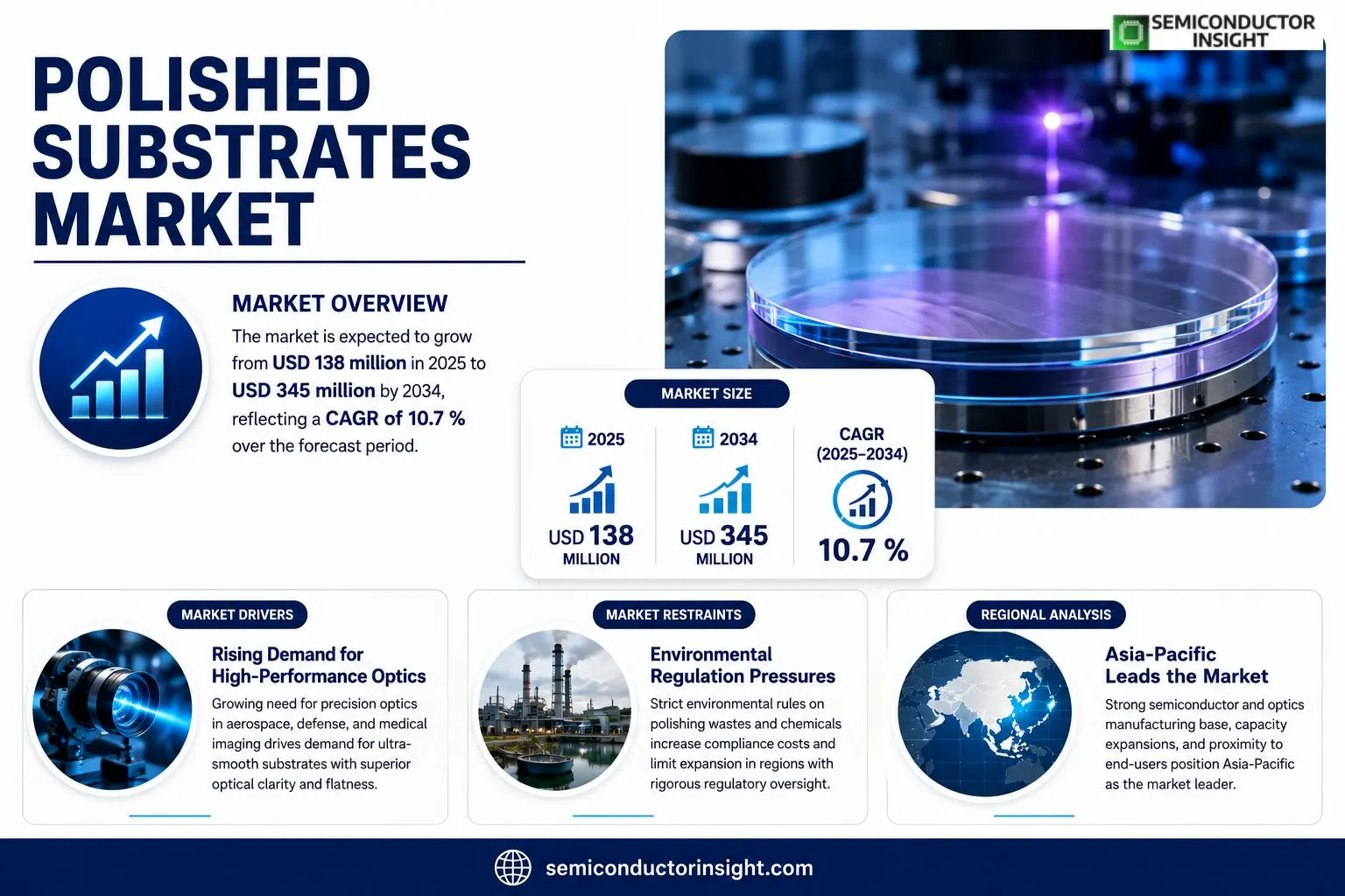
Polished Substrates market size was valued at USD 138 million in 2025. The market is expected to increase from USD 138 million in 2025 to USD 345 million by 2034, reflecting a compound annual growth rate of 10.7 % over the forecast period.
Polished substrates are optically flat or ultra‑smooth glass or ceramic components that act as foundational layers for photomask production, dense wavelength‑division multiplexing (DWDM) filters, and glass mastering applications.The rise of semiconductor lithography requirements, growing adoption of high‑precision optical elements in telecommunications, and continued capital investment in advanced manufacturing have stimulated demand for polished substrates. Leading suppliers such as Ohara, Edmund Optics, OPC Corporation, Schott and Tosoh Quartz dominate the landscape, while emerging projects focus on expanding capacity and improving surface quality.
MARKET DRIVERS
Rising Demand for High‑Performance Optics
Polished Substrates Market benefits from an expanding need for precision optics in aerospace, defense, and medical imaging. Customers increasingly require surfaces with nanometer‑level flatness to achieve tighter tolerances in laser systems and photonic devices. This pressure pushes manufacturers toward substrates that can be finished to superior optical clarity, boosting volume shipments.
Advances in Polishing Technologies
Recent breakthroughs in chemical‑mechanical polishing (CMP) and ultrafine abrasive formulations have shortened cycle times while preserving substrate integrity. Companies that adopt these methods can offer lower unit costs and faster time‑to‑market, making them attractive partners for OEMs seeking competitive advantage.
➤ Equipment automation and real‑time metrology are redefining throughput benchmarks, allowing producers to upscale capacity without sacrificing quality.
Because end‑users now prioritize reliability over price, the willingness to pay a premium for defect‑free polished wafers has risen. This price elasticity supports higher margin opportunities across the supply chain.
MARKET CHALLENGES
Stringent Surface‑Quality Specifications
Customers often impose sub‑nanometer roughness limits, which force suppliers to over‑invest in inspection equipment and clean‑room environments. The capital outlay can erode profitability for smaller players, limiting market entry.
Other Challenges
Material Compatibility
Certain high‑index glasses and semiconductor wafers react adversely to conventional slurry chemistries, leading to micro‑cracks and yield loss. Addressing this requires bespoke process development, adding complexity to production planning.
MARKET RESTRAINTS
Environmental Regulation Pressures
Regulatory bodies in Europe and North America have tightened limits on hazardous waste generated by polishing operations. Compliance demands expensive filtration and solvent‑recycling systems, which inflate operating costs and deter expansion in regions with stringent environmental oversight.Additionally, the shift toward greener manufacturing creates a competitive gap for firms that have not yet transitioned to low‑impact abrasive technologies, constraining their ability to win contracts that prioritize sustainability.
MARKET OPPORTUNITIES
Emerging Applications in Photonic Integrated Circuits
Photonic integrated circuits (PICs) require substrates with exceptionally smooth interfaces to minimize scattering losses. The growth of 5G infrastructure and data‑center interconnects fuels demand for PICs, opening a niche where polished substrates command premium pricing.Furthermore, collaborations between substrate manufacturers and AI‑driven process‑control firms are unlocking predictive polishing models. These models improve yield predictability and reduce scrap, presenting a clear pathway for cost‑effective scaling.
Polished Substrates Market Trends
Rising Demand for Ultra‑Precise Photomasks
Polished Substrates Market is currently being reshaped by a surge in demand for high‑precision photomasks used in advanced lithography. Semiconductor manufacturers are transitioning to nodes below 5 nm, where pattern fidelity depends on substrate flatness and surface cleanliness. Polished glass substrates, with sub‑nanometer roughness, satisfy those stringent specifications, prompting equipment suppliers to prioritize higher‑grade material inventories. Concurrently, the shift toward extreme ultraviolet (EUV) exposure tools amplifies the need for defect‑free surfaces, reinforcing the value chain of substrate polishers. This convergence of technology push and quality expectations is compelling vendors to invest in tighter process controls, ultimately elevating the competitive threshold for entrants.
Other Trends
DWDM Filter Expansion
The adoption of dense wavelength‑division multiplexing (DWDM) filters illustrates another growth vector. Telecom operators are expanding capacity on existing fiber plants to meet escalating data traffic, and polished substrates form the optical backbone of planar waveguide filters that separate tightly spaced channels. By leveraging the low‑scatter characteristics of high‑grade glass, filter manufacturers can achieve insertion loss levels below 0.2 dB, which translates directly into energy savings for network operators. As network operators pursue cost‑per‑bit reductions, the incentive to source substrates that support tighter channel spacing intensifies, prompting a modest but steady rise in order volumes from filter‑focused suppliers.
Shift Toward Asian Production Hubs
Geographic realignment towards Asian manufacturing hubs is becoming evident. Chinese and Taiwanese fabs have accelerated capital expenditure, creating a localized demand cluster for polished substrates that reduces lead times and logistics costs. Proximity to end‑users also enables rapid feedback loops between wafer producers and substrate finishers, fostering iterative improvements in surface quality. For Western players, the implication is a need to reassess supply‑chain strategies, either by establishing joint ventures in the region or by augmenting export capacities to remain relevant. The evolving geographic distribution therefore reshapes pricing dynamics and heightens the importance of flexible production footprints within Polished Substrates Market.
COMPETITIVE LANDSCAPE
Key Industry Players
Polished Substrates Market – Competitive Overview
The polished substrates arena is anchored by a handful of incumbents that together command the bulk of revenue. Ohara Corporation, benefiting from a vertically integrated supply chain and a long‑standing reputation in high‑purity glass, holds the largest share and sets pricing benchmarks for photomask and DWDM filter producers. Schott AG and Corning Inc. follow closely, leveraging extensive R&D budgets to push the limits of substrate flatness and surface defect control, thereby attracting premium‑grade customers in semiconductor lithography. The market shows a classic oligopolistic pattern: a few global giants dominate volume sales while smaller specialists carve out niches through differentiated surface finishes or rapid order‑to‑delivery cycles. This concentration reinforces entry barriers, as new entrants must invest heavily in precision polishing equipment and clean‑room certification to meet the exacting specifications demanded by high‑tech applications.Beyond the top three, a constellation of niche players adds depth to the competitive set. Edmund Optics sustains a strong foothold by coupling polished substrates with value‑added imaging optics, while OPC Corporation differentiates through proprietary quartz processing patents that lower defect density. Tosoh Quartz, Hoya Corp., and Zygo Corporation each target specific segments such as aerospace‑grade glass or ultra‑low‑expansion ceramics, exploiting specialized know‑how to win contracts that larger firms deem marginal. Smaller but agile firms like Jenoptik AG, Asahi Glass Co., Sumitomo Precision, and AGC Inc. compete on price‑performance ratios, often securing regional orders in Asia‑Pacific where proximity to end‑users reduces lead times. This layered competitive environment forces all participants to continuously refine product portfolios, explore strategic alliances, and invest in next‑generation polishing technologies to retain relevance.
List of Key Polished Substrates Companies Profiled
- Ohara Corporation
- Edmund Optics
- OPC Corporation
- Schott AG
- Tosoh Quartz
- Corning Inc.
- Hoya Corp.
- Zygo Corporation
- Jenoptik AG
- Asahi Glass Co.
- Sumitomo Precision
- AGC Inc.
Segment Analysis:
| Segment Category | Sub-Segments | Key Insights |
| By Type |
|
Glass Substrates
|
| By Application |
|
Photomasks
|
| By End User |
|
Semiconductor Equipment Makers
|
| By Process |
|
Chemical‑Mechanical Polishing (CMP)
|
| By Performance |
|
Low Defect Density
|
Regional Analysis: Polished Substrates Market
Asia‑Pacific
Recent plant expansions in Taiwan focus on sub‑micron polishing, while South Korea’s investment in clean‑room automation enables higher throughput without sacrificing defect control. The regional blend of mature fabs and newly built lines creates a tiered capacity that can serve both volume‑driven and specialty customers.
Semiconductor manufacturers dominate demand, yet solar‑module producers and advanced‑display makers are accelerating their procurement of polished substrates to meet tighter efficiency targets. Cross‑sector demand reinforces the resilience of the supply base.
Proximity of silica mines in China to polishing chemistry hubs in Japan shortens logistics cycles. Additionally, the rise of regional freight corridors reduces exposure to global shipping disruptions, allowing manufacturers to maintain just‑in‑time inventories.
Environmental standards in Japan and South Korea compel firms to adopt closed‑loop polishing systems, which in turn drive innovation in waste‑recovery technologies. Compliance has become a market entry criterion for many multinational buyers.
North America
In North America, Polished Substrates Market is anchored by a network of research‑intensive firms that prioritize incremental surface‑quality improvements for high‑performance chips. The United States leverages its intellectual‑property ecosystem to attract contracts that require ultra‑low‑defect densities, prompting suppliers to integrate AI‑assisted monitoring into their polishing stations. Customer expectations for rapid design cycles compel manufacturers to offer rapid‑prototype services, shifting the value proposition from pure volume to agility. Strategic alliances between substrate producers and defense contractors further elevate the importance of reliability in mission‑critical applications.
Europe
European stakeholders emphasize sustainability alongside precision, with Polished Substrates Market reflecting stringent EU directives on chemical usage and waste handling. Leading fabs in Germany and the Netherlands have pioneered water‑based polishing slurries, reducing volatile organic compound emissions. This environmental focus dovetails with a growing demand for high‑efficiency solar panels, where substrate surface flatness directly influences energy conversion rates. Consequently, firms that can certify eco‑compliant processes are better positioned to secure contracts with utilities and governmental renewable‑energy programs.
South America
South America remains a peripheral but increasingly relevant player, driven by emerging photovoltaic projects in Brazil and Chile. Local manufacturers are beginning to outsource polishing expertise to nearby Asian partners, creating a hybrid supply model that balances cost with technical competence. The region’s modest scale encourages collaborative ventures between substrate suppliers and regional universities, fostering a pipeline of talent equipped to handle next‑generation material requirements.
Middle East & Africa
In the Middle East and Africa, Polished Substrates Market is shaped by nascent semiconductor assembly lines and a burgeoning data‑center infrastructure. Governments are deploying incentives to attract foreign substrate producers, recognizing that surface‑quality control is a prerequisite for reliable high‑density memory modules. While the overall volume is limited, the strategic importance of establishing a local supply chain has spurred early‑stage joint‑venture agreements that could lay the groundwork for broader market participation in the coming decade.
Report Scope
This market research report provides a comprehensive analysis of the Polished Substrates Market , covering the forecast period 2026–2034. It offers detailed insights into market dynamics, technological advancements, competitive landscape, and key trends shaping the industry.
Key focus areas of the report include:
- Market Overview: The report begins with an overview outlining its current market scenario, key growth indicators, and industry transformation drivers. It discusses macroeconomic factors, demand–supply balance, regulatory landscape, and the strategic role of semiconductors in powering advancements across industries such as automotive, telecommunications, consumer electronics, and industrial automation.
- Market Size & Forecast: Historical data and future projections for revenue, unit shipments, and market value across major regions and segments.
- Segmentation Analysis: Detailed breakdown by product type, technology, application, and end-user industry to identify high-growth segments and investment opportunities.
- Regional Insights: Insights into market performance across North America, Europe, Asia-Pacific, Latin America, and the Middle East & Africa, including country-level analysis where relevant.
- Competitive Landscape: Profiles of leading market participants, including their product offerings, R&D focus, manufacturing capacity, pricing strategies, and recent developments such as mergers, acquisitions, and partnerships.
- Technology Trends & Innovation: Assessment of emerging technologies, integration of AI/IoT, semiconductor design trends, fabrication techniques, and evolving industry standards.
- Market Drivers & Restraints: Evaluation of factors driving market growth along with challenges, supply chain constraints, regulatory issues, and market-entry barriers.
- Stakeholder Insights: Insights for component suppliers, OEMs, system integrators, investors, and policymakers regarding the evolving ecosystem and strategic opportunities.
Primary and secondary research methods are employed, including interviews with industry experts, data from verified sources, and real-time market intelligence to ensure the accuracy and reliability of the insights presented.
FREQUENTLY ASKED QUESTIONS:
What is the current market size of Polished Substrates Market?
-> Polished Substrates Market was valued at USD 125 million in 2024 and is expected to reach USD 255 million by 2031 at a CAGR of 11.0%.
Which key companies operate in Polished Substrates Market?
-> Key players include Ohara, Edmund Optics, OPC Corporation, Schott, Tosoh Quartz, among others.
What are the key growth drivers?
-> Key growth drivers include demand for photomasks, DWDM filters, and glass mastering applications.
Which region dominates the market?
-> Asia is the leading region, driven primarily by strong demand in China.
What are the emerging trends?
-> Emerging trends include advanced photomask technology, high‑performance DWDM filter development, and innovative glass mastering processes.

Get Sample Report PDF for Exclusive Insights
Report Sample Includes
- Table of Contents
- List of Tables & Figures
- Charts, Research Methodology, and more...
 Download Sample Report PDF



