Key Statistics
Key Takeaways
- Market trajectory: The 2026 value is USD 2,090 million, with a 2036 outlook of USD 6,437 million and 11.9% compound growth. Physical-layer licensing and associated implementation services benefit from DDR5 server refreshes and HBM4 accelerator interfaces, while memory device and controller revenue remain outside this defined category.
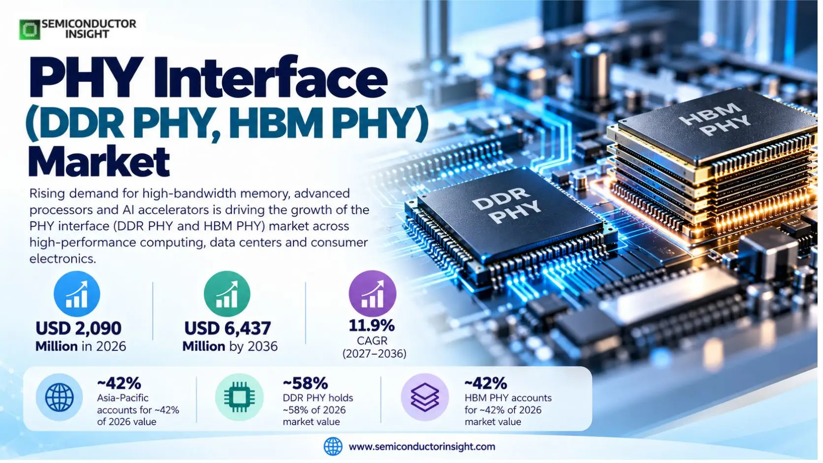
- DDR PHY mix: DDR PHY retains an estimated ~58% of 2026 economic value because DDR5 and LPDDR implementations span server, client, mobile and embedded silicon. HBM PHY, at ~42%, has the higher modeled growth rate of ~15.0% as 2,048-I/O HBM4 connections raise integration difficulty.
- Application demand: AI accelerators and GPUs represent an estimated ~35% of 2026 PHY demand, with data-center servers at ~30%. These are distinct interface sockets: accelerators favor stacked HBM physical links, while host processors commonly integrate DDR5 or LPDDR physical layers.
- Regional concentration: Asia-Pacific leads with an estimated ~42% of 2026 market value and modeled ~13.1% annual growth, reflecting Korean HBM design, Taiwanese foundry implementation and Asian SoC production. North America represents an estimated ~31% through major IP suppliers and accelerator designers.
- Commercial boundary: A PHY performs electrical signaling, clock alignment, training and data integrity, while a memory controller schedules commands. HBM4 controller releases, memory stack shipments and UCIe chiplet announcements indicate design activity but cannot be counted wholesale as standalone PHY revenue.
PHY Interface (DDR PHY, HBM PHY) Market Overview
PHY interface (DDR PHY and HBM PHY) market was valued at USD 2,090 million in 2026 and is projected to reach USD 6,437 million by 2036, expanding at a CAGR of 11.9% during 2027–2036. Asia-Pacific accounted for an estimated ~42% of 2026 value, while HBM PHY design intensity rises as HBM4 and HBM4E enter accelerator programs.
A memory physical layer translates digital controller intent into signals that can survive real package traces, dense interposers and DRAM input/output circuits. DDR PHYs train read and write timing across printed circuit board routes, whereas HBM PHYs coordinate thousands of fine-pitch connections close to accelerator logic. These functions demand analog and mixed-signal design, delay calibration, voltage and temperature compensation, and extensive silicon characterization, so production-qualified PHY blocks have substantial engineering value beyond their RTL interfaces.
Commercial revenue covers licensed hard PHY macros, directly attributable PHY customization and the economic value of proprietary PHY development embedded in memory subsystems. It does not include complete HBM stacks, DDR DIMMs, standalone controller licenses, accelerator chips, packaging substrates or unrelated SerDes. Synopsys identifies its DDR5/4 PHY as a GDSII-delivered hard macro with an embedded calibration processor and DFI 5.0 controller interface; that product definition illustrates why the physical layer must be separated from the command scheduler that connects to it.
The first demand engine is the server memory transition. DDR5 interfaces require read and write leveling, data-eye training, deskew and on-die calibration that exceed the integration burden of earlier DDR generations. Synopsys specifies DDR5/4 PHY operation up to 8,400 Mbps, while Cadence has described a 12.8Gbps DDR5 memory IP product line. The precise supported rate depends on process, package and system topology, but every new SoC generation can create fresh PHY qualification and implementation work.
The second engine is accelerator memory bandwidth. Cadence introduced a 12.8Gbps HBM4 PHY and controller solution in April 2025, with a hardened PHY targeted to TSMC N3 and N2 nodes. HBM4 doubles the interface width to 2,048 I/Os, making signal timing, power distribution and interposer co-design central to accelerator tapeouts. Samsung began commercial HBM4 shipments in February 2026, while Micron described HBM4 production for next-generation AI platforms in March 2026; those milestones support the timing of PHY integration demand rather than directly measuring PHY license revenue.
A third change is interface specialization. Cadence announced LPDDR6/5X 14.4Gbps memory IP in July 2025 and subsequently described an LPDDR5X reliability-oriented design for data centers, broadening the contexts in which low-power physical layers are deployed. The DFI 6.0.1 specification discussed in July 2026 supports newer DDR, LPDDR and HBM protocols. At the same time, UCIe 3.0 increases chiplet-link performance, but a UCIe PHY is a separate die-to-die interface and is excluded from DDR/HBM PHY market totals.
Segment Analysis: By Type
The primary type split assigns an estimated ~58% of 2026 value to DDR PHY and ~42% to HBM PHY. The two groups are distinguished by memory signaling topology, not by controller software: DDR links typically connect an SoC to board-level or package-level memory, whereas HBM PHY supports dense stack connections on an advanced package. The modeled HBM share expands as HBM4 raises bus width and memory bandwidth.
| Type | Function | Market position |
|---|---|---|
| DDR PHY (DDR4, DDR5, LPDDR) | Estimated ~58% of 2026 modeled type value. DDR PHY addresses DDR4/DDR5 DIMM channels and low-power LPDDR mobile or edge SoCs. For DDR4/DDR5 DIMM channels and low-power LPDDR mobile or edge SoCs, the PHY block must maintain usable sampling windows while supply voltage, process variation and thermal load change during operation. A mature but broad socket base sustains licenses across server processors, consumer application processors and embedded controllers. For A mature but broad socket base sustains licenses across server processors, consumer application processors and embedded controllers., commercial buyers evaluate silicon proof, process-node support, memory-device interoperability and validation collateral because interface failure can force a complete redesign. | Estimated ~58% of 2026 modeled type value. DDR PHY addresses the largest installed diversity of memory-interface sockets. For the largest installed diversity of memory-interface sockets, the PHY block must maintain usable sampling windows while supply voltage, process variation and thermal load change during operation. DDR5 brings more complex training and validation, while LPDDR5X and LPDDR6 create power-sensitive designs in devices and newer server form factors. For DDR5 brings more complex training and validation, while LPDDR5X and LPDDR6 create power-sensitive designs in devices and newer server form factors., commercial buyers evaluate silicon proof, process-node support, memory-device interoperability and validation collateral because interface failure can force a complete redesign. |
| HBM PHY (HBM2, HBM2E, HBM3) | Estimated ~42% of 2026 modeled type value. HBM PHY addresses stacked memory on GPU, AI accelerator and HPC silicon. For stacked memory on GPU, AI accelerator and HPC silicon, the PHY block must maintain usable sampling windows while supply voltage, process variation and thermal load change during operation. HBM4 and HBM4E extend the original HBM2/HBM3 taxonomy and introduce 2,048 I/O pins, demanding package-aware power and timing closure. For HBM4 and HBM4E extend the original HBM2/HBM3 taxonomy and introduce 2,048 I/O pins, demanding package-aware power and timing closure., commercial buyers evaluate silicon proof, process-node support, memory-device interoperability and validation collateral because interface failure can force a complete redesign. | Estimated ~42% of 2026 modeled type value. HBM PHY addresses higher-value advanced-node and interposer implementations. For higher-value advanced-node and interposer implementations, the PHY block must maintain usable sampling windows while supply voltage, process variation and thermal load change during operation. The modeled growth rate is ~15.0%, above DDR PHY, because accelerator projects pay for advanced-node qualification, power optimization and interoperability. For The modeled growth rate is ~15.0%, above DDR PHY, because accelerator projects pay for advanced-node qualification, power optimization and interoperability., commercial buyers evaluate silicon proof, process-node support, memory-device interoperability and validation collateral because interface failure can force a complete redesign. |
DDR and HBM physical-layer implementation economics
The modeled DDR PHY category covers the legacy DDR4 interface as well as DDR5 and LPDDR families, without treating each subprotocol as a separate full-market revenue total. DDR5 PHY requires training of timing margins on board-level routes, while LPDDR emphasizes power states and compact package layouts. HBM PHY uses an entirely different dense interposer interface and earns higher engineering value per qualified advanced-node design; this contrast explains the diverging modeled growth trajectories.
The annual type allocation below is an analyst-modeled revenue trajectory in USD million rather than a disclosure of measured vendor licensing sales. DDR PHY begins at an estimated ~58% and HBM PHY at ~42% in 2026, with their differentiated growth assumptions calibrated to reproduce the global 2036 forecast. Each value reflects the same exclusive revenue boundary, so DRAM device turnover, UCIe physical layers and separate memory controllers are not added to the totals.
| Year | DDR PHY (DDR4/DDR5/LPDDR) | HBM PHY (HBM2/HBM2E/HBM3) |
|---|---|---|
| 2026 | 1,212.2 | 877.8 |
| 2027 | 1,322.5 | 1,009.2 |
| 2028 | 1,442.9 | 1,160.2 |
| 2029 | 1,574.2 | 1,333.8 |
| 2030 | 1,717.4 | 1,533.4 |
| 2031 | 1,873.7 | 1,762.9 |
| 2032 | 2,044.2 | 2,026.8 |
| 2033 | 2,230.2 | 2,330.1 |
| 2034 | 2,433.2 | 2,678.8 |
| 2035 | 2,654.6 | 3,079.7 |
| 2036 | 2,896.2 | 3,540.6 |
Process-node allocation and memory interface qualification
Advanced nodes below 7nm account for an estimated ~55% of 2026 modeled PHY value, mainstream 7nm–28nm nodes ~34%, and mature nodes above 28nm ~11%. These proportions represent the value of qualified IP implementations, not semiconductor wafer volume. HBM4 hardened PHY availability on TSMC N3 and N2 supports advanced-node value concentration, while DDR4 and industrial LPDDR designs continue to sustain qualification activity at older foundries.
Process portability is not a matter of moving RTL alone. Hard macros embed foundry-specific transistors, I/O cells, clock networks, delay lines and analog receiver circuits, so a node migration often triggers characterization and silicon validation. The annual values below apply a fixed modeled process-node mix to the reconciled global trajectory; they illustrate economic exposure by implementation class and should not be interpreted as independently observed foundry licensing figures.
| Year | Advanced Nodes (Below 7nm) | Mainstream Nodes (7nm to 28nm) | Mature Nodes (Above 28nm) |
|---|---|---|---|
| 2026 | 1,149.5 | 710.6 | 229.9 |
| 2027 | 1,286.4 | 795.2 | 257.3 |
| 2028 | 1,439.5 | 889.9 | 287.9 |
| 2029 | 1,610.9 | 995.8 | 322.2 |
| 2030 | 1,802.7 | 1,114.4 | 360.5 |
| 2031 | 2,017.3 | 1,247.1 | 403.5 |
| 2032 | 2,257.5 | 1,395.5 | 451.5 |
| 2033 | 2,526.2 | 1,561.7 | 505.2 |
| 2034 | 2,827.0 | 1,747.6 | 565.4 |
| 2035 | 3,163.6 | 1,955.7 | 632.7 |
| 2036 | 3,540.2 | 2,188.5 | 708.0 |
Deployment-model distribution and licensing structure
Licensed hard IP accounts for an estimated ~64% of modeled 2026 economic value, licensed soft IP ~17%, and custom in-house PHY development ~19%. The latter represents attributed engineering value rather than invoices from external vendors. Synopsys explicitly describes DDR5/4 PHY as a GDSII hard macro, while controller interfaces are often provided as RTL; mixing those different delivery formats would overstate the soft-PHY category.
Hard PHY providers sell proven electrical implementations and bring-up support; soft-IP engagement generally centers on configurable digital assistance and interfaces, while internal teams develop specialized physical circuitry for high-volume proprietary platforms. The annual allocation below is a modeled economic-equivalent segmentation in USD million and uses the same worldwide base and forecast totals, avoiding double counting with complete memory controllers or DRAM chips.
| Year | Licensed Hard IP | Licensed Soft IP | Custom In-House PHY Development |
|---|---|---|---|
| 2026 | 1,337.6 | 355.3 | 397.1 |
| 2027 | 1,496.9 | 397.6 | 444.4 |
| 2028 | 1,675.1 | 444.9 | 497.3 |
| 2029 | 1,874.5 | 497.9 | 556.5 |
| 2030 | 2,097.7 | 557.2 | 622.7 |
| 2031 | 2,347.4 | 623.5 | 696.9 |
| 2032 | 2,626.9 | 697.8 | 779.9 |
| 2033 | 2,939.6 | 780.8 | 872.7 |
| 2034 | 3,289.6 | 873.8 | 976.6 |
| 2035 | 3,681.2 | 977.8 | 1,092.9 |
| 2036 | 4,119.5 | 1,094.2 | 1,223.0 |
Segment Analysis: By Application
The application model assigns an estimated ~35% to AI accelerators and GPUs, ~30% to data-center servers, ~14% to HPC, ~17% to consumer and mobile, and ~4% to other systems. AI and server sockets overlap in the same infrastructure but are allocated by the actual chip carrying the physical layer, avoiding double counting a host DDR5 interface and an accelerator HBM interface.
| Application | Demand characteristics |
|---|---|
| AI Accelerators & GPUs | Estimated ~35% of 2026 application value. AI Accelerators & GPUs programs procure or develop PHY capability for HBM4-enabled accelerator tapeouts with dense interposer connections and memory-stack interoperability testing. For AI Accelerators & GPUs, physical-layer qualification is tied to the package and process, while the memory controller implements command scheduling and error handling. Within AI Accelerators & GPUs, the commercial implication is a distinct mix of hard-macro licenses, silicon validation, customization and continuing support across successive SoC design wins. A memory device sale is not counted as PHY IP revenue. |
| Data Center Servers | Estimated ~30% of 2026 application value. Data Center Servers programs procure or develop PHY capability for DDR5 channels on CPUs, server SoCs and infrastructure processors requiring deterministic training and RAS integration. For Data Center Servers, physical-layer qualification is tied to the package and process, while the memory controller implements command scheduling and error handling. Within Data Center Servers, the commercial implication is a distinct mix of hard-macro licenses, silicon validation, customization and continuing support across successive SoC design wins. A memory device sale is not counted as PHY IP revenue. |
| High-Performance Computing (HPC) | Estimated ~14% of 2026 application value. High-Performance Computing (HPC) programs procure or develop PHY capability for large scientific-computing processors balancing bandwidth, latency and package thermal limits. For High-Performance Computing (HPC), physical-layer qualification is tied to the package and process, while the memory controller implements command scheduling and error handling. Within High-Performance Computing (HPC), the commercial implication is a distinct mix of hard-macro licenses, silicon validation, customization and continuing support across successive SoC design wins. A memory device sale is not counted as PHY IP revenue. |
| Consumer Electronics & Mobile Devices | Estimated ~17% of 2026 application value. Consumer Electronics & Mobile Devices programs procure or develop PHY capability for LPDDR5X and LPDDR6 interfaces in phones, tablets and mobile compute with stringent idle-power requirements. For Consumer Electronics & Mobile Devices, physical-layer qualification is tied to the package and process, while the memory controller implements command scheduling and error handling. Within Consumer Electronics & Mobile Devices, the commercial implication is a distinct mix of hard-macro licenses, silicon validation, customization and continuing support across successive SoC design wins. A memory device sale is not counted as PHY IP revenue. |
| Others | Estimated ~4% of 2026 application value. Others programs procure or develop PHY capability for automotive compute, networking ASICs and specialized industrial memory subsystems with long qualification cycles. For Others, physical-layer qualification is tied to the package and process, while the memory controller implements command scheduling and error handling. Within Others, the commercial implication is a distinct mix of hard-macro licenses, silicon validation, customization and continuing support across successive SoC design wins. A memory device sale is not counted as PHY IP revenue. |
A typical AI server can contain several separate memory interfaces: the CPU has DDR5 or LPDDR channels, the accelerator package has HBM physical links, and network processors can contain their own DDR interfaces. Allocation by silicon device and physical-layer socket is therefore more reliable than treating all data-center equipment spending as PHY demand. The application trajectories below are calibrated to the same 2026 base and 2036 forecast and preserve the five original end-use classes.
The modeled application split also reflects technology timing. HBM4 shipments and HBM4E controller announcements intensify advanced-node accelerator work in 2026, while DDR5 remains the larger recurring host-compute deployment base. LPDDR6/5X development creates future mobile and data-center design opportunities, but the physical-layer licensing value is not interchangeable with memory-stack shipment value or the bill of materials for complete AI servers.
Regional Analysis
Asia-Pacific holds the largest modeled 2026 share at ~42%, followed by North America at ~31%, Europe at ~16%, Latin America at ~6%, and Middle East & Africa at ~5%. These estimates allocate memory-interface IP engineering and licensing value, not physical memory shipments or data-center hardware spending. The regional pattern reflects where accelerator designs, foundry implementations and proprietary memory-interface engineering are executed.
How does geography shape DDR PHY and HBM PHY licensing demand?
Asia-Pacific combines foundry implementation and memory manufacturing, North America combines licensable PHY suppliers and accelerator design, Europe favors industrial and automotive reliability, Latin America remains linked to imported computing platforms, and the Middle East and Africa are predominantly downstream system adopters. Each geography therefore has a different route to memory-interface economic value, even though the same HBM4 or DDR5 technology may be deployed in servers worldwide.
| Region | Position | Growth outlook | Demand profile | What decides supplier selection |
|---|---|---|---|---|
| Asia-Pacific | Largest (~42%) | ~13.1% CAGR | PHY design and qualification | Licensing, process-node validation and customer design ownership |
| North America | Second (~31%) | ~11.6% CAGR | PHY design and qualification | Licensing, process-node validation and customer design ownership |
| Europe | Developing (~16%) | ~10.5% CAGR | PHY design and qualification | Licensing, process-node validation and customer design ownership |
| Latin America | Developing (~6%) | ~12.4% CAGR | PHY design and qualification | Licensing, process-node validation and customer design ownership |
| Middle East & Africa | Developing (~5%) | ~5.5% CAGR | PHY design and qualification | Licensing, process-node validation and customer design ownership |
Competitive Landscape and Semiconductor IP Positioning
The competitive center consists of firms with production-qualified DDR or HBM memory-interface IP and the silicon-validation capability to support new foundry nodes. Synopsys and Cadence document direct PHY products, while Rambus demonstrates complementary memory-controller IP that can be paired with third-party PHYs. Several other profiled firms participate through adjacent DRAM, SerDes, controller or design services and are not assumed to be direct suppliers of standalone HBM PHY licenses.
Synopsys competes through hardened DDR5/4 PHY delivery, training features and DFI controller interoperability. Its published 8,400Mbps DDR5/4 PHY capability and GDSII deliverable establish a direct commercial product boundary. Cadence addresses a broader memory-IP subsystem, with its 12.8Gbps HBM4 PHY for TSMC N3/N2 and 14.4Gbps LPDDR6/5X implementation demonstrating advanced-node and protocol-generation coverage. The competitive advantage is silicon proof and integration support rather than a nominal protocol checklist alone.
Rambus illustrates why a memory-controller company must be evaluated carefully in a PHY market. Its March 2026 HBM4E controller announcement supports 16Gbps per pin and explicitly permits pairing with a third-party or customer PHY. That establishes a complementary, sometimes bundled, commercial relationship but does not turn all controller revenue into physical-layer licensing. Suppliers able to validate interoperability across both layers can still influence PHY selection through subsystem qualification and reference designs.
Samsung, SK hynix and Micron shape interface specifications through HBM stack development, testing and internal base-die engineering. Their 2025–2026 HBM4 milestones establish technical requirements for third-party accelerator PHYs, yet their memory device revenue is outside this market. Likewise, firms focused on UCIe SerDes, embedded storage PHY or general design services may be relevant partners without a verified production DDR5 or HBM4 hard macro. Buyer due diligence should distinguish demonstrated memory PHY from adjacent interface competence.
Commercial competition is strongest at the intersection of foundry qualification, analog expertise, controller interoperability and post-silicon support. A customer can change the digital controller architecture more easily than a hardened analog PHY tied to an advanced node and package, creating switching costs after tapeout. Multi-generation support, interoperability testing and detailed power-integrity models can therefore justify licensing premiums even when a competitor advertises comparable nominal transfer rates.
Tier structure
| Tier | Companies | Basis of competition |
|---|---|---|
| Direct PHY IP suppliers | Synopsys; Cadence Design Systems | Direct DDR/HBM physical-layer product descriptions, hardened macros, memory training features and foundry-specific implementation support provide a strong basis for customer evaluation. Competitive differentiation rests on demonstrated silicon, data rate, power efficiency, validation coverage and the ability to help a customer reach production rather than simply delivering a specification-compliant digital model. The same design win may require extensive pre-silicon and post-silicon work. |
| Controller and interface complements | Rambus; Alphawave Semi; Marvell/Inphi; Arasan; Mobiveil | This group participates in memory-controller, high-speed connectivity or related IP ecosystems, but direct HBM PHY offerings are not established for every named company. Rambus explicitly describes third-party PHY pairing for its HBM4E controller, so competitive assessment must separate controller licensing from the hardened electrical interface and avoid double counting subsystem revenue. Foundry compatibility and end-to-end validation can still make complementary providers influential partners. |
| Memory makers and specialist design ecosystem | Samsung; SK hynix; Micron; CEVA; Kandou; Dolphin Design; Hardent; Open-Silicon | HBM device makers, adjacent interface designers and specialist engineering firms affect memory-interface standards, test vehicles and implementation choices. Their presence in the profiled roster reflects ecosystem influence rather than evidence that each sells a standalone DDR5 or HBM4 PHY macro. The commercial question is whether a supplier owns licensable physical-layer IP or contributes complementary memory, packaging, verification or design services. |
Key companies profiled
- Synopsys, Inc.
- Cadence Design Systems, Inc.
- Rambus Inc.
- Alphawave Semi
- Marvell Technology Group Ltd. (Inphi)
- Samsung Electronics Co., Ltd.
- SK Hynix Inc.
- Micron Technology, Inc.
- Arasan Chip Systems Inc.
- Mobiveil Inc.
- CEVA, Inc.
- Kandou Bus SA
- Dolphin Design
- Hardent Inc.
- Open-Silicon (A Sievert Company)
Technology Development and Qualification Economics
PHY commercialization begins with protocol requirements and ends with silicon-verified electrical behavior in a customer package. Hard-macro suppliers must characterize receiver equalization, delay tracking, clock distribution, power delivery and thermal stability at the target process node. DDR5 and HBM4 impose different physical problems, so an experienced interface team cannot assume a single PHY macro will be portable across both technologies. Against a global 2026 benchmark of USD 2,090 million and a 2036 forecast of USD 6,437 million, the 11.9% growth outlook depends on how many interface blocks require new analog hardening and verification rather than on the dollar value of complete DRAM or accelerator products.
DDR5 PHY validation focuses on channel training across board-level routes, DIMM topologies, rank configurations and temperature variation. Synopsys describes read/write leveling, data-eye training, per-bit deskew and an embedded calibration processor in its DDR5/4 PHY. These features translate into paid engineering work when a customer changes a package, memory topology or foundry node, and they explain why hardened PHY deliverables include physical views and test collateral rather than only RTL.
HBM4 changes the design problem by doubling the memory interface to 2,048 I/Os and increasing per-pin throughput. Cadence described a 12.8Gbps HBM4 PHY, interposer reference design, controller and lab bring-up environment in April 2025. The physical interface must satisfy high-bandwidth timing and power limits while fitting the accelerator floorplan, and advanced-node hard macros require foundry-specific characterization. These constraints raise the value of successful silicon validation and packaging co-design.
Newer standards also change integration boundaries. DFI 6.0.1 addresses DDR5, LPDDR6 and HBM4 controller-to-PHY communication, while UCIe 3.0 specifies 48/64GT/s chiplet links. Both matter to complex systems, but only the DDR/HBM physical layer is counted here. A chiplet accelerator may contain both UCIe and HBM interfaces; treating every die-to-die link as HBM PHY would distort application shares and exaggerate the addressable market.
Market Dynamics, Drivers, Restraints and Opportunities
Memory-interface demand grows as SoCs adopt faster memory standards and require more process-specific validation. The market faces opposing forces: HBM4 and DDR5 expand high-value engineering opportunities, while license concentration, foundry migration cost and system qualification delays restrain adoption. The impact factors below allocate modeled percentage-point effects across the 2027–2036 outlook and reconcile to the headline growth rate.
MARKET DRIVERS
Drivers Impact Analysis*
| Market Drivers | Impact Rank | CAGR Contribution (%) | 2027–2029 | 2030–2032 | 2033–2036 |
|---|---|---|---|---|---|
| HBM4 and HBM4E accelerator integration | High | +5.40% | High | High | Medium |
| DDR5 server and LPDDR interface refresh | High | +4.20% | High | Medium | Medium |
| Advanced-node hard-macro qualification | Medium-High | +3.10% | High | High | Medium |
| AI custom silicon and heterogeneous packaging | Medium | +2.70% | Medium | High | High |
| Improved controller-PHY interoperability | Medium | +1.40% | Medium | High | Medium |
| Others (automotive memory and industrial edge redesigns) | Low | +0.80% | Low | Medium | Medium |
HBM4 widens the accelerator interface
HBM4 moves to 2,048 I/O connections and higher data rates, making package-aware timing, signal integrity and power delivery more demanding than HBM3-class designs. Cadence introduced a 12.8Gbps HBM4 PHY in April 2025, while Samsung, SK hynix and Micron disclosed HBM4 product milestones across 2025 and 2026. These events support a modeled ~15.0% HBM PHY growth trajectory because each accelerator generation requires qualified interface integration rather than a simple software update.
DDR5 and LPDDR preserve broad socket demand
DDR PHY accounts for an estimated ~58% of 2026 value because it serves host processors, mobile SoCs, embedded controllers and infrastructure chips. DDR5 requires calibration and training features that improve timing margins at high speeds, while LPDDR5X and LPDDR6 extend the need for power-sensitive physical layers. Cadence described a 14.4Gbps LPDDR6/5X subsystem in July 2025, and Synopsys documents DDR5/4 PHY operation up to 8,400Mbps.
Foundry qualification raises integration value
A hardened PHY cannot be moved from one node to another without physical redesign and verification of analog behavior, clocking, I/O circuits and package assumptions. Cadence targets HBM4 PHY hard macros at TSMC N3 and N2, while DDR5/4 hard PHYs are delivered as physical layouts with calibration firmware. As the advanced-node segment reaches an estimated ~55% of 2026 economic value, qualified implementation support becomes a major differentiator for silicon IP vendors.
Custom accelerator programs multiply interface variants
Hyperscale and specialist AI designers increasingly optimize memory channels around particular workloads, package layouts and power budgets. The application model assigns ~35% of 2026 value to AI accelerators and GPUs and ~30% to data-center servers, reflecting separate HBM and DDR interface sockets within one infrastructure system. Custom designs create additional opportunities for PHY tuning and silicon validation, although server hardware spending itself is excluded from the market boundary.
MARKET RESTRAINTS
Restraints Impact Analysis*
| Market Restraints | Impact Rank | CAGR Contribution (%) | 2027–2029 | 2030–2032 | 2033–2036 |
|---|---|---|---|---|---|
| Cost and risk of analog silicon qualification | High | -2.50% | High | High | Medium |
| Concentration among production-proven IP suppliers | Medium-High | -1.70% | High | Medium | Medium |
| Licensing and advanced-node access constraints | Medium | -1.00% | Medium | High | Medium |
| Others (protocol overlap and long integration cycles) | Low | -0.50% | Medium | Low | Low |
Silicon validation is expensive and time-consuming
Analog memory interfaces must be validated across process, voltage, temperature, DRAM vendor behavior and package routes. A timing or power-integrity issue discovered after tapeout can require costly silicon changes, discouraging smaller chip teams from developing new PHY variants. The market consequently favors reusable, production-qualified hard macros but still bears substantial nonrecurring engineering cost each time a supplier moves to a new process or memory generation.
Concentrated suppliers constrain design choice
Only a limited set of providers demonstrate broad production-ready DDR or HBM PHY portfolios across advanced nodes. Synopsys and Cadence publish direct physical-layer specifications, while Rambus describes controller IP that can connect to third-party PHYs. Customers may face switching costs after integration and package co-design, and license negotiations can become concentrated around a small number of foundry-qualified options for each process and memory standard.
Export controls and foundry access shape licensing
Advanced-node memory interfaces require design tools, process design kits and silicon qualification capacity that are not equally accessible in every market. Cross-border technology controls can affect who may license or implement the newest PHY hard macros. A regional market may therefore show strong demand for AI servers while supporting relatively little direct PHY design value, reinforcing the importance of assigning revenue to actual licensing and engineering activity.
MARKET OPPORTUNITIES
DFI standardization reduces subsystem friction
DFI 6.0.1 provides an updated controller-to-PHY communication framework for DDR5, LPDDR6 and HBM4. That common interface can help chip teams change controller suppliers or integrate memory subsystems with less digital protocol rework, while preserving the need for physical silicon qualification. IP vendors able to supply compliant verification environments, calibration firmware and package guidance can earn incremental integration value around the hardened PHY license.
LPDDR enters new high-efficiency computing contexts
Low-power memory is increasingly relevant beyond smartphones as AI servers and edge platforms seek favorable performance per watt. Cadence introduced LPDDR6/5X 14.4Gbps IP in 2025 and described an LPDDR5X reliability-oriented implementation for data-center use in early 2026. These developments create PHY design opportunities with distinct power-management and error-handling requirements, but do not justify counting complete LPDDR DRAM sales as interface IP revenue.
Thermal-aware HBM base-die integration
Samsung described D2D PHY thermal challenges in its 2026 HBM4E technology communications, highlighting how concentrated signaling activity creates heat within advanced memory base dies. As HBM4E pushes toward higher speeds, PHY suppliers and accelerator designers can differentiate through power distribution, clock efficiency and package thermal co-design. Such services may increase engineering value per design even when the number of accelerator projects grows more slowly than headline AI infrastructure investment.
Value Chain, Licensing Channels and Integration Workflow
The PHY interface value chain links protocol standards, IP development, foundry hardening, chip design, package co-design and post-silicon bring-up. Its commercial output is an electrical interface that works at the customer’s required memory speed and thermal envelope, not the memory chip itself. Supplier selection therefore involves both intellectual-property rights and evidence that the macro operates in a realistic system.
Specification and design. Memory protocol evolution defines the electrical and timing target, but suppliers must translate that target into analog silicon capable of surviving package and process variation. DDR5 training, LPDDR low-power modes and HBM4 high-density signaling impose different design constraints. Qualified hard IP often carries substantial characterization collateral, and engineering teams rely on that evidence to reduce tapeout risk and shorten the path from interface selection to production.
Foundry implementation. Hardened PHY macros use process-specific transistor models, I/O cells and physical verification views. Cadence has identified TSMC N3 and N2 targets for HBM4, while Synopsys describes DDR5/4 GDSII delivery. A migration to a new node or package may require substantial rework even when the digital controller protocol is unchanged, creating repeat opportunities for qualified analog IP and design-support contracts.
Customer integration. A chip designer must reconcile the controller-to-PHY protocol, memory vendor characteristics, board or interposer topology and system power budget. Rambus HBM4E controller IP can pair with a third-party PHY, illustrating the separate procurement decisions that may occur inside a complete memory subsystem. Integration teams value common verification environments, training firmware and realistic test chips because interoperability failures can undermine the whole accelerator or processor design.
Post-silicon lifecycle. After tapeout, engineers measure signal eyes, train timing parameters, validate memory combinations and tune reliability across voltage and temperature. New DRAM speeds and packaging configurations can generate further characterization work even for a previously licensed macro. Support revenue and implementation services are included only when directly attributable to the memory PHY; complete DRAM stacks, controller-only licenses and unrelated die-to-die SerDes remain outside the market boundary.
Recent Developments in DDR and HBM PHY Interfaces
- 18 Apr 2025 HBM4 PHY
Cadence introduced a 12.8Gbps HBM4 PHY and controller solution, including a hardened PHY aimed at TSMC N3 and N2 and a reference interposer test chip. The announcement matters because HBM4 doubles interface width to 2,048 I/Os and makes electrical validation a larger part of accelerator integration. The controller and PHY are separate deliverables, so the development supports physical-layer design demand without converting full subsystem revenue into PHY sales. Source - 16 Jun 2025 Foundry IP
Cadence expanded its Samsung Foundry collaboration and multi-year memory/interface IP agreement covering SF4X, SF5A and SF2P nodes. The disclosed portfolio includes DDR5, LPDDR and other interfaces, showing how process-specific PHY qualification is becoming a recurring design requirement. The commercial implication is broader access to hardened memory-interface implementations and integration collateral for AI, automotive and connectivity silicon. Source - 09 Jul 2025 LPDDR6 PHY
Cadence announced a 14.4Gbps LPDDR6/5X memory IP system tapeout, combining a configurable hardened PHY with a soft controller. This is relevant because higher LPDDR speeds and low-power operating modes require new physical validation, even when a customer retains familiar digital interfaces. The design also broadens LPDDR beyond mobile devices into AI infrastructure and heterogeneous packages, increasing the range of potential PHY integration contracts. Source - 12 Sep 2025 HBM4 memory
SK hynix announced completion of HBM4 development and readiness for mass production, following earlier 12-layer sample shipments. The event is a memory-device milestone rather than a PHY license disclosure, but it provides a clear timing signal for accelerator interface qualification. Designers integrating HBM4 must verify wide I/O connections, package timing and power budgets against production-capable memory stacks. Source - 13 Jan 2026 LPDDR reliability
Cadence described a data-center-oriented LPDDR5X 9600Mbps memory IP solution using Microsoft RAIDDR error correction. The announcement shows that low-power memory interfaces are being adapted for reliability-sensitive infrastructure, not solely battery-powered mobile devices. PHY design teams must reconcile electrical efficiency with system error handling and validation, supporting new hard-macro integration opportunities while keeping controller and DRAM device value separate. Source - 12 Feb 2026 HBM4 shipment
Samsung began commercial HBM4 shipments using a 4nm logic base die and a 2,048-I/O interface. This product milestone confirms a practical demand environment for next-generation accelerator physical layers and interposer validation. The market impact is heightened qualification pressure on chip designers and PHY vendors, not a direct measure of memory-interface licensing because Samsung reports memory device activity. Source - 04 Mar 2026 HBM4E controller
Rambus launched HBM4E controller IP supporting up to 16Gbps per pin and 4.1TB/s per memory device, explicitly stating that the controller can pair with a third-party PHY. This distinction is commercially important because it validates separate procurement of command/control logic and the electrical physical layer. Future HBM4E accelerator designs may therefore create additional integration and interoperability work for PHY providers. Source - 16 Mar 2026 HBM4 production
Micron announced volume shipment of HBM4 36GB 12-high memory for a next-generation NVIDIA platform, reporting more than 11Gbps per-pin speeds and over 2.8TB/s bandwidth. This establishes another production-capable HBM4 memory option that accelerator teams must qualify. PHY demand arises from interoperable electrical links and package co-design; the memory shipment itself remains outside standalone interface-IP revenue. Source
REPORT SCOPE & SEGMENTATION
| Attribute | Details |
|---|---|
| Base Year | 2026 |
| Estimated Year | 2027 |
| Forecast Year | 2036 |
| Forecast Period | 2027–2036 |
| Historical Data | 2021–2025 |
| Market Definition | DDR/LPDDR and HBM physical-layer IP licenses, directly attributable implementation support, and modeled proprietary PHY engineering economic value. |
| Unit | USD million |
| By Type | DDR PHY (DDR4 PHY, DDR5 PHY, LPDDR PHY) · HBM PHY (HBM2 PHY, HBM2E PHY, HBM3 PHY) |
| By Application | AI Accelerators & GPUs · Data Center Servers · High-Performance Computing (HPC) · Consumer Electronics & Mobile Devices · Others |
| By End User | Semiconductor IP Licensees (Fabless & IDM Chipmakers) · Cloud & Hyperscale Data Center Operators · Consumer Electronics OEMs |
| By Process Node | Advanced Nodes (Below 7nm) · Mainstream Nodes (7nm to 28nm) · Mature Nodes (Above 28nm) |
| By Deployment Model | Licensed Hard IP · Licensed Soft IP · Custom In-House PHY Development |
| By Region | Five-region exclusive modeled allocation, 2026 base year; regional values describe interface IP economic activity, not DRAM or full system sales. Asia-PacificChina, Taiwan, South Korea, Japan, India and Southeast Asia North AmericaUnited States and Canada EuropeGermany, France, Netherlands, United Kingdom and rest of Europe Latin AmericaBrazil, Mexico and rest of Latin America Middle East & AfricaSaudi Arabia, UAE, South Africa and rest of region |
| Key Companies Profiled | Synopsys, Inc. · Cadence Design Systems, Inc. · Rambus Inc. · Alphawave Semi · Marvell Technology Group Ltd. (Inphi) · Samsung Electronics Co., Ltd. · SK Hynix Inc. · Micron Technology, Inc. · Arasan Chip Systems Inc. · Mobiveil Inc. · CEVA, Inc. · Kandou Bus SA · Dolphin Design · Hardent Inc. · Open-Silicon (A Sievert Company) |
| Customization Scope | Country and node-specific PHY licensing, vendor design-win mapping, HBM4 and LPDDR6 qualification programs, controller-to-PHY interoperability, package implementation costs and scenario sensitivity for 2027–2036. |
Frequently Asked Questions
What is the global DDR PHY and HBM PHY interface market size?
The modeled 2026 market value is USD 2,090 million, rising to USD 6,437 million by 2036 with a 11.9% compound growth rate over 2027–2036. The category includes the physical-layer IP and attributable integration work needed to connect memory controllers to DDR, LPDDR and HBM devices. It excludes the value of DRAM stacks, complete processors and standalone controller licenses.
Which region leads PHY interface revenue?
Asia-Pacific leads with an estimated ~42% of 2026 economic value, supported by Taiwanese advanced-node implementation and Korean HBM engineering. North America follows at ~31% through major PHY IP vendors and accelerator designers, while Europe contributes ~16%. These shares are modeled allocations of design and licensing activity rather than observed market-wide vendor disclosures or regional memory-chip shipments.
Which physical-layer type has the largest share?
DDR PHY represents an estimated ~58% of 2026 modeled value because DDR4, DDR5 and LPDDR interfaces serve a broad installed range of host processors, mobile SoCs and embedded devices. HBM PHY contributes ~42% and has faster modeled growth of ~15.0%, reflecting the increasing complexity of accelerator memory links and the transition toward HBM4 and HBM4E.
How does a PHY differ from a memory controller?
The PHY implements the electrical transmitter, receiver, clocking, calibration and training circuitry needed for reliable data movement. A controller schedules commands, refresh, access policy and memory protocol transactions. Synopsys documents a DDR5/4 hard PHY connected over DFI 5.0, while Rambus notes that its HBM4E controller can pair with third-party PHY solutions. Their revenues should not be counted twice.
Why is HBM4 important for interface IP demand?
HBM4 expands the interface to 2,048 I/Os and raises signaling speed, increasing the need for package-aware timing closure, power integrity and silicon interoperability. Cadence disclosed a 12.8Gbps HBM4 PHY for TSMC N3 and N2 in April 2025, while Samsung and Micron described commercial HBM4 production in 2026. Those events indicate more qualification activity rather than a directly measured PHY licensing market.
What role does DDR5 play in the forecast?
DDR5 remains a major source of interface licensing and qualification because server and client platforms require updated PHYs with timing training and signal-integrity features. Synopsys describes DDR5/4 PHY support up to 8,400Mbps with read/write leveling and per-bit deskew. The broad range of DDR and LPDDR sockets helps explain why DDR PHY retains an estimated ~58% of 2026 value despite faster HBM growth.
Are UCIe physical layers included in this market?
No. UCIe is a die-to-die chiplet interconnect standard, whereas DDR and HBM PHYs connect memory controllers to DRAM devices or stacked memory interfaces. The UCIe Consortium describes 48/64GT/s rates in version 3.0, but those chiplet PHY sales belong to a separate economic category. An accelerator package can contain both technologies without making their interface revenues interchangeable.
What does the advanced-node segment represent?
Advanced process nodes below 7nm account for an estimated ~55% of 2026 modeled PHY economic value, compared with ~34% at 7nm–28nm and ~11% above 28nm. These are allocations of interface implementation value rather than wafer volume. Hardened HBM4 PHY support for TSMC N3 and N2 illustrates the high-value qualification work concentrated in leading-edge processes.
Which companies provide direct DDR or HBM PHY IP?
Synopsys and Cadence publish explicit DDR or HBM PHY hard-macro offerings with technical specifications and integration support. Rambus is a significant memory controller and subsystem participant, but its HBM4E release specifically describes pairing with a third-party PHY. Samsung, SK hynix and Micron shape memory interface requirements through DRAM products; they should not automatically be treated as standalone external PHY licensors.
What are the principal growth constraints?
The main constraints are analog silicon qualification cost, dependence on a small number of production-proven vendors, advanced-node access restrictions and lengthy memory interoperability testing. A PHY must work across process, voltage, temperature and package variations, and a failed interface can force expensive tapeout revisions. These costs favor proven hard macros but limit the number of suppliers and new designs that can enter the market.
Research Sources & Evidence Base
Get Sample Report PDF for Exclusive Insights
Report Sample Includes
- Table of Contents
- List of Tables & Figures
- Charts, Research Methodology, and more...
 Download Sample Report PDF