Photonics Epitaxial Wafers Market Insights
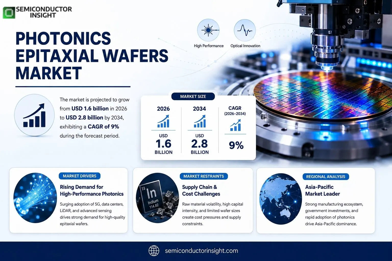
Photonics Epitaxial Wafers market was valued at USD $1.6 billion in 2026 and is expected to reach USD $2.8 billion by 2034, registering a CAGR of approximately 9% over the forecast period.
Photonics epitaxial wafers are crystalline substrates produced through metal‑organic chemical vapor deposition or molecular beam epitaxy on compound semiconductors such as GaAs or InP; they serve as the foundation for high‑performance light‑emitting diodes, laser diodes and photonic integrated circuits employed across telecommunications, sensing technologies and LED display systems.This evolution underscores opportunities for stakeholders seeking resilience within supply chains amid accelerating demand for advanced optical communication infrastructure worldwide.
MARKET DRIVERS
Rising Demand for High‑performance Photonic Components
The evolution of optical networking and 5G infrastructure has created a surge in need for precision photonic devices that can sustain higher bandwidths while remaining power efficient. Within this landscape, photonic epitaxial wafers form the backbone of lasers, photodetectors, and modulators whose performance hinges on crystalline perfection. photonics market is experiencing a compound annual growth rate that has outpaced many adjacent semiconductor sectors, driven in part by the rapid deployment of data centers and the demand for long‑haul fiber links. Companies that can deliver wafers with ppm‑level defect densities are positioned to capture premium pricing, as customers focus on yield and reliability over raw production volume. Moreover, governments are investing heavily in national digital infrastructure projects, allocating multi‑billion‑dollar budgets to strengthen high‑speed connectivity, which directly translates into increased component orders. The convergence of telecommunications, automotive lidar, and industrial sensing further broadens the customer base for photonic wafers, creating a diversifying demand matrix that counterbalances cycle volatility in any single industry segment.
Advancements in Epitaxial Growth Techniques
Recent breakthroughs in metal‑organic chemical vapor deposition (MOCVD) and molecular beam epitaxy (MBE) have lowered barriers to entry for firms seeking to produce high‑grade epitaxial wafers. Innovations such as surface‑passivation layers, epitaxial lateral overgrowth, and in‑situ monitoring of stoichiometry allow manufacturers to fine‑tune bandgaps and reduce threading dislocations to sub‑micron levels. This technological maturation enables the scaling of wafers from 100 mm to 300 mm formats without a proportional rise in defect counts, thereby optimizing material utilization and reducing per‑unit costs. Moreover, the adoption of silicon‑on‑insulator (SOI) platforms for photonic integration has opened avenues for monolithic hybrid circuits, blurring the line between electronic and photonic fabrication and creating new market niches. The cost advantages observed in early adopters suggest that firms exploiting these process economies can expect a more favorable gross margin profile over the next decade, reinforcing the attractiveness of photonic epitaxial wafers for both OEMs and contract manufacturers.
➤ Manufacturers that secure early access to these advanced growth methodologies will likely eclipse competitors by up to 15 % in yield, translating into a higher market share and improved profitability.
Beyond technology, the momentum in the Photonics Epitaxial Wafers Market is also powered by strategic collaborations between hardware vendors and world‑class research institutions. Joint venture agreements, technology transfer initiatives, and shared pilot projects accelerate the commercialisation of next‑generation devices that rely on wafer‑scale platforms, such as quantum communication modules and terahertz sensors. These collaborations not only validate the efficacy of the underlying fabrication processes but also provide a pipeline of skill‑set development that ensures a well‑trained workforce for scaling production. The combination of rising component demand, process innovation, and collaborative ecosystems positions the market for a sustained upward trajectory, with path‑forged opportunities for firms that can align their production capacities with the pace of technological evolution.
MARKET CHALLENGES
Supply Chain Vulnerabilities in Raw Materials
The manufacture of photonic epitaxial wafers demands an uninterrupted supply of ultra‑pure gases, high‑purity precursors, and crystalline substrates that often originate from a handful of specialized suppliers. The geopolitical concentration of these critical inputs has exposed the market to disruptions precipitated by trade tensions, natural disasters, and regulatory changes. Small‑to‑mid‑size manufacturers, in particular, encounter margin pressure when confronted with volatile pricing for gallium, arsenic, and indium. Even slight increases in raw material costs can erode profitability, given the thin margin buffers in high‑precision wafer production. Furthermore, the fragility of downstream logisticsparticularly shipping timetables for temperature‑sensitive precursorsamplifies the risk that production schedules will be throttled, leading to backlogs that can ripple across the entire supply chain.
Other Challenges
Market Consolidation and Pricing Pressures
The concentration of a few dominant players in the manufacturer base creates a competitive environment where pricing engines are heavily influenced by economies of scale. New entrants often face significant upfront capital expenditures and must contend with established firms that possess entrenched relationships with lead suppliers, thereby consolidating market share. This dynamic can suppress price growth, making it difficult for smaller operators to sustain profitability. Additionally, the commoditisation of select photonic components, such as Si‑based modulators, has begun to erode value‑recapture opportunities, prompting fiscal strain on companies that rely on refresh cycles to service customer demand. Sustained pressure from both competitors and customers will likely intensify pricing strategies in 2027, compelling firms to seek differentiation through performance metrics rather than cost competition alone.
MARKET RESTRAINTS
High Capital Expenditure Barriers
Launching or expanding a photonic epitaxial wafer fabrication line entails capital outlays that surpass a billion dollars when factoring in advanced MOCVD or MBE suites, high‑temperature furnaces, and stringent clean‑room infrastructure. The financial risk associated with such investments, compounded by the long lead times required to achieve mature yields, creates a natural restraint for new market entrants. Venture capital reallocation towards complementary fields, such as silicon photonics, also diverts potential funding pools. As a result, the industry’s developable footprint remains limited to a handful of geographically dispersed facilities, curtailing the rate at which product availability can be aligned with global demand spikes.
MARKET OPPORTUNITIES
Emerging Applications in Autonomous Vehicles
The autonomous driving sector is demanding photonic systems capable of generating and detecting high‑resolution laser beams for lidar, cameralens, and range‑finding applications. Photonic epitaxial wafers that support miniature, energy‑efficient laser arrays are becoming integral to meeting the stringent cost and packaging constraints of commercial vehicles. This convergence offers firmware‑agnostic opportunities for wafer suppliers to tap into vehicle‑to‑everything (V2X) data exchanges. Given that automotive manufacturers are adopting stringent sensor reliability standards, the exposure of vendors to supply‑chain audits encourages the development of traceable, defect‑controlled wafer linesfostering a mutually beneficial relationship . The projected market for automotive lidar modules is poised to exceed 10 billion euros by 2030, creating a robust revenue layer for providers of photonic epitaxial wafers that can meet the sector’s ballistic performance thresholds.Furthermore, the steady migration of 6G research initiatives towards high‑frequency, millimetre‑wave radars & photonic super‑resolution receivers envisions the necessity for ultra‑wideband-compatible wafers. Firms that can deliver custom‑grade, low‐defect substrates for these front‑end devices stand to gain a competitive advantage as telecommunications operators invest in ubiquitous next‑generation access networks. The co‑location of photonic wafer laboratories within data‑center campuses enables rapid prototyping and accelerated go‑to‑market timelines, further incentivising capital commitments in this niche. Deployment of these wafers extends beyond the circular ranks of pure telecom, heralding an expanding horizon of specialized use cases across radar, sensing, and quantum information. In aggregate, the intertwined opportunity tapestry demands a proactive investment strategy from leaders willing to build out the necessary process repertoire, harness intellectual property, and secure early access to strategic partner pipelines.
Photonics Epitaxial Wafers Market Trends
Dominant Shift Toward InP‑Based Wafer Adoption
Over the last several years, indium phosphide-based epitaxial wafers have surged past gallium arsenide counterparts in both volume and the range of sophisticated applications. This reversal stems from proven gains in laser diode efficiency, higher-speed modulators, and quantum-dot emitters that now underpin next-generation data-center optics and 5‑G/6‑G wireless links. InP substrates also cope better with high-temperature processing, allowing OEMs to pursue denser integration without sacrificing thermal dissipation. As a result, manufacturing shifts concentrate on regions with mature InP supply chains, while capital moves toward advanced tooling. Companies that can tame raw-material cost pressures and precision alignment hurdles will be able to secure a larger slice of the growing photonics wafer segment.
Other Trends
Emerging Demand from Integrated Photonic Circuits in Data Centers
Integrated photonic circuitry inside data-center racks has become a reliable driver for wafer demand. By embedding optical interconnects directly onto a silicon substrate, operators replace copper traces with low-loss waveguides, achieving higher bandwidth while cutting power consumption. This trend has persuaded leading foundries to expand their photonic wafer portfolios, particularly in the 480 Gbps and beyond categories. The resulting competitive pressure forces suppliers to accelerate yield-improvement programs and halve defect rates. Market participants who can deliver high-yield InP wafers at scale will find themselves positioned to capture the emerging customer base of hyperscale operators.
Emerging Regional Concentration in East Asia
Notably, the cultivation of photonic wafer ecosystems in East Asia has accelerated in tandem with the region’s dominance in high-speed photonics manufacturing. Concentrated resources in China, Japan, and South Korea propel these locales to the forefront of InP wafer production, leveraging local supply chains and policy support for optical infrastructure. Concurrently, Southeast Asian packaging hubs are developing the necessary assembly services to close the value chain. For firms targeting these markets, proximity to R&D centers and access to low-cost skilled labor present unique opportunities. Conversely, the region’s intense competition demands continuous improvement in fabrication throughput and cost efficiency. Companies that can navigate these operating parameters will be able to maintain relevance as the East Asian photonic wafer market continues to mature.
COMPETITIVE LANDSCAPE
Key Industry Players
Photonics Epitaxial Wafers Market Industry Analysis
II‑VI Incorporated maintains the upper echelon of photonics epilayer landscape, commanding roughly 35 % of the $US$ 2.4 billion market in 2026. The company’s integrated supply chainfrom raw III‑V compound crystals to final wafer deliveryensures consistent process control, thereby underpinning higher yield and reduced defect rates. Its aggressive acquisition of InP wafer specialists in 2023 further tightens its foothold in the LiDAR and high‑speed data‑center arenas, where precision and repeatability are paramount. This concentration of capability translates into a competitive moat that pressures smaller entrants to either co‑manufacture or diversify into emerging niche applications, reshaping the market’s cost structure and innovation cycle.Beyond II‑VI, a cohort of niche manufacturersIQE, Visual Photonics Epitaxy Co., and Nichia Corpdrive specialized supply chains targeting discrete photonics segments. IQE’s focus on high‑power GaAs LEDs for automotive illumination and Visual Photonics’ GaN‐based heterostructure lines for infrared imaging inject fresh technical differentiation into the corridor. These firms, alongside Cree’s semiconductor integration expertise and Samsung OES’s high‑volume InP production, are characterized by shorter development cycles and localized partnerships with OEMs. Their nimble structure enables rapid adaptation to shifting application demands such as 5G photonics and quantum communication. For larger players, the proliferation of such agile competitors underscores the need for strategic alliances and shared technology platforms to maintain market share and sustain profitability.
List of Key Photonics Companies Profiled
- II‑VI Incorporated
- IQE
- Visual Photonics Epitaxy Co.
- LandMark Optoelectronics
- SCIOCS
- Semiconductor Wafer Inc
- Nichia Corp
- Cree
- Samsung OES
- Mitsubishi Electric
- Skyworks Solutions
- Lumenis
Segment Analysis:
| Segment Category | Sub-Segments | Key Insights |
| By Type |
|
GaAs dominates due to its superior electron mobility and high‑efficiency optoelectronic properties; it is a cornerstone of high‑speed laser diodes and optical amplifiers; its resilience to high‑temperature operation makes it attractive for aerospace and defense applications. |
| By Application |
|
Infrared Imaging leads with its ability to integrate tightly with photonic sensor arrays; it benefits from wafer‑scale uniformity to reduce fabrication variance; its high spectral sensitivity supports advanced thermal imaging used in automotive safety and industrial inspection. |
| By End User |
|
Telecommunications dominates due to the growing demand for high‑capacity fiber networks; photonic wafers enable compact, high‑performance laser sources and amplifiers; their reliability supports 5G and beyond infrastructure deployments. |
| By Fabrication Approach |
|
MOCVD leads with high throughput and cost‑effective deposition of compound semiconductors; it supports doping gradients essential for optical bandwidth tailoring; its maturity drives adoption in large‑scale quantum cascade laser production. |
| By Device Architecture |
|
Conventional Wafer remains preferred for its compatibility with standard photonic fabrication lines; it allows seamless integration of multiple active devices on a single substrate; its robustness supports scalable manufacturing of high‑density sensor arrays. |
Regional Analysis: Photonics Epitaxial Wafers Market
Asia-Pacific
The clustering of large‑scale fabs reduces lead times and enhances supply resilience, creating a self‑reinforcing cycle of output and innovation in photonic paving.
Collaborations between academia and industry accelerate the adoption of alternative substrate materials, boosting device performance across telecom and sensing sectors.
Strategic inventory buffers and localized component sourcing mitigate international freight volatility, ensuring a steady wafer supply for time‑sensitive photonics projects.
Harmonised regional standards and investment incentives underpin the capacity of firms to stay ahead in the photonics epitaxial wafers market without disruptive compliance overheads.
North America
North America remains a critical engine for photonics wafer demand, particularly in the data‑centre and radar markets. The United States, with its strong venture‑backed ecosystem, is home to several high‑performance photonic research labs that translate foundational findings into market‑ready components. The region’s emphasis on secure communications infrastructure creates steady downstream demand for high‑integrity photonic devices, feeding into a robust downstream wafer supply chain. However, a tighter focus on semiconductor self‑sufficiency prompts a slow shift toward domestic wafer fabrication, which may compress profit margins for global players. Firms that navigate this transition by establishing joint‑venture fabrication facilities within the region can tap into both patriotic procurement slots and access to advanced fabrication equipment. In Europe, the convergence of photonics and critical national security technologies sees increased public‑private partnership projects, driving demand for specialized epitaxial wafers that support the continent’s high‑bandwidth ambitions. Together, North America and Europe create a dual‑chain supply model that balances innovation thrust against policy‑driven security imperatives, shaping a competitive yet risk‑managed market landscape.
Europe
Europe’s photonics wafer prospects are shaped by the convergence of telecom infrastructure upgrades and the automotive supply‑chain’s maturity. The continent’s increasing focus on sustainable, high‑bandwidth data pathways is encouraging phasing‑in of silicon‑photonic interconnects, thereby creating downstream wafer consumption. Simultaneously, growing demand for automotive lidar and imaging in autonomous systems is driving smaller wafer orders with higher performance expectations. European policy initiatives, especially related to digital sovereignty, mandate a shift toward domestic wafer manufacturing for high‑security components. Opportunistic collaborations between European photonics designers and foundries are accelerating the technology diffusion curve, but the relatively high cost of capital investment remains a barrier to rapid scaling. Firms that establish localized supply partnerships can respond swiftly to regulatory demands while benefiting from closer collaboration with lead system integrators in the telecommunications space.
South America
South America is an emerging, albeit nascent, contributor to the photonics epitaxial wafers landscape. The region’s large natural gas infrastructure and expansion of renewable energy farms create a niche for high‑efficiency optical monitoring systems, prompting a modest upsurge in wafer demand. Nevertheless, the capacity to produce epitaxial wafers domestically is limited, and the region relies heavily on imports for critical photonic substrates. The resultant dependency exposes firms to global price swings and supply chain delays, which dampens long‑term growth prospects. Yet, partnerships initiated with multinational wafer manufacturers are generating local workforce development and technology transfer, laying groundwork for incremental production capabilities. Over the next decade, incremental policy incentives focusing on technology diversification could spur growth in this segment, though the pace remains slower relative to more developed markets.
Middle East & Africa
The Middle East & Africa region stands at an operational crossroads, where emerging data‑centre clusters and advanced manufacturing initiatives are beginning to influence the photonics wafer market. Qatar and UAE have already invested in next‑generation internet backbone projects, requiring high‑bandwidth photonic interconnects, which in turn generate a small but growing downstream demand for premium epitaxial wafers. Meanwhile, abundant solar resource across Africa has spurred interest in optical sensors for grid monitoring, creating early demand for low‑cost photonic substrates. However, infrastructural constraints and a limited local fabrication ecosystem mean that most wafer procurement continues to route through Asia‑Pacific and North American suppliers. The region’s ability to attract foreign direct investment into wafer fabrication plants is contingent upon stable regulatory frameworks and sovereign incentives. As global trade dynamics shift toward localisation, practitioners in the Middle East & Africa will need to balance imported technology reliance with strategic captive manufacturing to stay competitive in a tightening market.
Report Scope
This market research report provides a comprehensive analysis of the Photonics Epitaxial Wafers Market , covering the forecast period 2026–2034. It offers detailed insights into market dynamics, technological advancements, competitive landscape, and key trends shaping the industry.
Key focus areas of the report include:
- Market Overview: The report begins with an overview outlining its current market scenario, key growth indicators, and industry transformation drivers. It discusses macroeconomic factors, demand–supply balance, regulatory landscape, and the strategic role of semiconductors in powering advancements across industries such as automotive, telecommunications, consumer electronics, and industrial automation.
- Market Size & Forecast: Historical data and future projections for revenue, unit shipments, and market value across major regions and segments.
- Segmentation Analysis: Detailed breakdown by product type, technology, application, and end-user industry to identify high-growth segments and investment opportunities.
- Regional Insights: Insights into market performance across North America, Europe, Asia-Pacific, Latin America, and the Middle East & Africa, including country-level analysis where relevant.
- Competitive Landscape: Profiles of leading market participants, including their product offerings, R&D focus, manufacturing capacity, pricing strategies, and recent developments such as mergers, acquisitions, and partnerships.
- Technology Trends & Innovation: Assessment of emerging technologies, integration of AI/IoT, semiconductor design trends, fabrication techniques, and evolving industry standards.
- Market Drivers & Restraints: Evaluation of factors driving market growth along with challenges, supply chain constraints, regulatory issues, and market-entry barriers.
- Stakeholder Insights: Insights for component suppliers, OEMs, system integrators, investors, and policymakers regarding the evolving ecosystem and strategic opportunities.
Primary and secondary research methods are employed, including interviews with industry experts, data from verified sources, and real-time market intelligence to ensure the accuracy and reliability of the insights presented.
FREQUENTLY ASKED QUESTIONS:
What is the current market size of Photonics Epitaxial Wafers Market?
->Photonics Epitaxial Wafers market was valued at USD $1.6 billion in 2026 and is expected to reach USD $2.8 billion by 2034, registering a CAGR of approximately 9% over the forecast period.
What is the projected market size of Photonics Epitaxial Wafers Market by 2034?
-> The Photonics Epitaxial Wafers Market is projected to reach USD million by 2034.
What is the CAGR for the Photonics Epitaxial Wafers Market?
-> The Photonics Epitaxial Wafers Market is expected to grow at a CAGR of % during the forecast period.
How does the semiconductor market compare in size and growth?
-> semiconductor market was estimated at USD 579 billion in 2022 and is projected to reach USD 790 billion by 2029, growing at a CAGR of 6% during the forecast period.
Which wafer types dominate the Photonics Epitaxial Wafers market?
-> The market is segmented by type, primarily including GaAs and InP.
What are the major application segments for Photonics Epitaxial Wafers?
-> Key application segments include 3D Sensing, Infrared Imaging, Telecommunications and Data communications, and LED Displays.
Which region currently holds the largest share of the Photonics Epitaxial Wafers market?
-> Regional segmentation covers North America, Europe, Asia, South America, and Middle East & Africa with the inclusion of major countries such as the US, China, Germany, and India.
Which companies are the top players in the Photonics Epitaxial Wafers market?
-> Major players include II-VI Incorporated, LandMark Optoelectronics, IQE, Visual Photonics Epitaxy Co. Ltd, SCIOCS, and Semiconductor Wafer Inc.
What are the primary growth drivers for the Photonics Epitaxial Wafers market?
-> Key growth drivers include the rising demand for advanced photonics applications in IoT-based electronics, automotive-specific Analog applications, and power management solutions.
What emerging trends are influencing the Photonics Epitaxial Wafers market?
-> Emerging trends include the development of Hybrid MPUs and MCUs for real-time embedded processing, advances in discrete power devices, and the integration of AI/IoT into photonics manufacturing processes.
How are pricing and revenue trends shaping the market?
-> Market pricing and revenue trends are influenced by the latest semiconductor design trends, fabrication techniques, and the strategic role of advanced materials in photonics production.
Get Sample Report PDF for Exclusive Insights
Report Sample Includes
- Table of Contents
- List of Tables & Figures
- Charts, Research Methodology, and more...
 Download Sample Report PDF