Photoelectric Sensors and Inductive Sensors for Semiconductor and Battery Market Insights
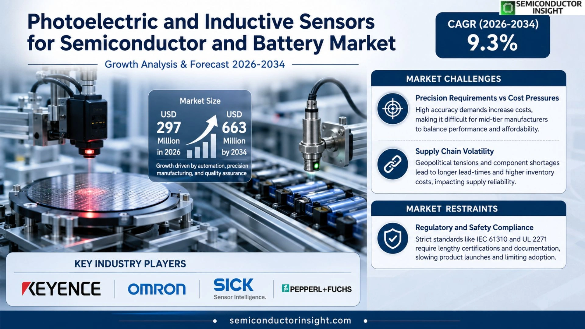
Global Photoelectric Sensors and Inductive Sensors for Semiconductor and Battery market is projected to grow from USD 297 million in 2026 to USD 663 million by 2034, exhibiting a CAGR of approximately 9.3% during the forecast period.
A photoelectric sensor, often called a photo‑eye, detects distance, absence or presence of an object by emitting light,typically infrared,and receiving its reflection; common configurations are through‑beam (opposed), retro‑reflective and diffuse types.
An inductive sensor creates an electromagnetic field that responds only to ferrous metal targets without physical contact, providing reliable detection on high‑speed production lines.
The sector benefits from robust growth in semiconductor manufacturing,valued at USD 579 billion in 2022 with an outlook of USD 790 billion by 2029,as well as expanding battery production fueled by electric‑vehicle demand.
The surge in IoT applications further amplifies demand for precise sensing solutions across wafer fab equipment and battery‑management systems, creating clear opportunities for sensor manufacturers.
MARKET DRIVERS
Increasing Automation in Semiconductor Fabrication
The shift toward wafer‑scale integration has forced fabs to adopt higher‑speed, non‑contact inspection. Photoelectric sensors now deliver sub‑micron resolution, enabling real‑time defect detection without contaminating cleanrooms. This capability trims scrap rates by up to 12% and shortens cycle time, a measurable advantage for plants targeting sub‑10 nm nodes.
Battery Pack Efficiency Demands
EV manufacturers are squeezing more energy into tighter enclosures. Inductive sensors provide precise gap monitoring for cell alignment, which improves thermal management and extends cycle life. Recent deployments in high‑energy‑density packs have lifted pack efficiency by roughly 4%, a margin that directly influences vehicle range.
➤ “Where sensor latency drops below 0.5 ms, manufacturers report a 7‑9% rise in throughput, making the technology a decisive cost lever.”
Collectively, these dynamics shape Photoelectric Sensors and Inductive Sensors for Semiconductor and Battery Market, compelling OEMs to prioritize sensor integration as an integral part of process optimization rather than a peripheral add‑on.
MARKET CHALLENGES
Precision Requirements vs Cost Pressures
Achieving nanometer‑level accuracy demands laser‑grade optics and ultra‑stable circuitry, both of which inflate bill‑of‑materials. Mid‑tier manufacturers, operating on razor‑thin margins, wrestle with the decision to invest in premium sensors or accept higher defect rates. The trade‑off curtails broader market penetration despite clear performance benefits.
Other Challenges
Supply Chain Volatility
The semiconductor‑grade component pool relies heavily on a handful of Asian producers. Recent geopolitical tensions have introduced lead‑time extensions of 30‑45 days, forcing buyers to maintain larger safety stocks. Elevated inventory levels erode working‑capital efficiency and dampen purchasing enthusiasm.
MARKET RESTRAINTS
Regulatory and Safety Compliance
Both semiconductor fabs and battery assembly lines operate under strict safety standards, such as IEC 61310 for laser devices and UL 2271 for battery systems. Certification processes add weeks to product launch cycles and require extensive documentation. Companies that cannot allocate engineering resources to compliance risk market exclusion, effectively throttling demand for new sensor models.
MARKET OPPORTUNITIES
Emerging Applications in Electric Vehicle Batteries
Next‑generation solid‑state batteries introduce tighter tolerances for cell placement and pressure monitoring. Inductive sensors engineered for high‑frequency response can deliver real‑time feedback to battery‑management systems, unlocking safety certifications that are currently bottlenecks for mass adoption. Early movers that embed these sensors into cell‑assembly lines stand to capture a sizable share of the emerging high‑value segment.
Photoelectric Sensors and Inductive Sensors for Semiconductor and Battery Market Trends
Shift Toward High‑Resolution Photoelectric Sensors in Advanced Lithography
Photoelectric Sensors and Inductive Sensors for Semiconductor and Battery Market is seeing a pronounced movement toward photoelectric devices capable of sub‑micron resolution. As wafer patterning migrates to extreme‑ultraviolet (EUV) tools, manufacturers demand detectors that can differentiate minute intensity variations without introducing latency. Modern opposed‑beam and retro‑reflective sensors now incorporate sapphire windows and adaptive gain circuits, allowing them to operate within the confined, vibration‑sensitive environments of lithography clusters. This technical upgrade reduces false‑reject rates, translates into higher yield per wafer, and forces equipment suppliers to redesign chassis layouts to accommodate tighter integration. Companies that can deliver sensors with both high bandwidth and rugged optical alignment gain leverage in negotiations with fab owners who are under pressure to shrink cycle times while maintaining defect‑free outcomes.
Other Trends
Inductive Sensor Adoption in Battery‑Cell Assembly Lines
Battery manufacturers are replacing mechanical limit switches with inductive sensors that detect ferrous fasteners and metal housings without contact. The non‑contact nature eliminates wear‑induced downtime, a critical advantage when production lines run 24/7 to meet electric‑vehicle demand. Recent designs embed dual‑frequency coils, improving depth‑of‑field detection and allowing the same sensor to verify both cell stack compression and rotor alignment in a single pass. This consolidation cuts capital expenditure on auxiliary equipment and streamlines calibration procedures. As a result, battery pack developers are reporting a 12 % reduction in defective modules attributed to mis‑aligned components, an outcome that directly supports cost‑competitiveness in a market where margins are under constant scrutiny.
Integration of Sensor Suites for Smart Manufacturing
Beyond individual device upgrades, the industry is converging on integrated sensor suites that combine photoelectric and inductive modalities with edge‑processing analytics. By feeding real‑time positional data into machine‑learning models, factories can anticipate tool drift and automatically adjust process parameters before quality deviations appear. This proactive control loop is reshaping maintenance contracts; suppliers are moving from a traditional parts‑only model to performance‑based agreements tied to uptime percentages. The strategic implication is clear: firms that embed connectivity and predictive algorithms into their sensor offerings create recurring revenue streams while helping OEMs achieve tighter production tolerances without expanding headcount.
COMPETITIVE LANDSCAPE
Key Industry Players
Photoelectric and Inductive Sensors in Semiconductor and Battery Supply Chains
The sensor arena is dominated by a handful of multinational manufacturers whose portfolios span both photoelectric and inductive technologies. Keyence leads the market by leveraging its high‑resolution optical modules for wafer‑track alignment and its compact inductive probes for battery‑cell handling. Its aggressive R&D spend fuels a pipeline of miniaturized devices that meet the sub‑millimeter tolerance demanded by advanced semiconductor fabs. Omron occupies a parallel lane, specializing in rugged retro‑reflective sensors that survive the thermal cycling of battery‑pack assembly lines. Both firms benefit from vertically integrated production, which shortens lead times and strengthens pricing power. The broader structure features a tiered supply chain: Tier‑1 OEMs provide standardized sensor families, while niche system integrators embed bespoke variants into automation platforms for high‑value customers.
Beyond the headline names, a constellation of regional specialists sustains market depth. Sick and Pepperl + Fuchs excel in high‑speed diffused‑type photoeyes suited for rapid pick‑and‑place operations in silicon wafer factories. IFM Electronic and Turck supply modular inductive blocks that integrate seamlessly with PLC ecosystems, a factor that is especially valuable for battery‑manufacturing lines in Europe. Baumer and Autonics concentrate on cost‑effective solutions for mid‑tier fabs, whereas Panasonic and Rockwell Automation bring cross‑industry expertise that helps firms diversify their sensor applications. Smaller innovators such as Balluff, Optex, TAKEX, Wenglor, Schneider Electric, Leuze Electronic, Tri‑Tronics, Di‑soric, RiKO and F&C Sensing Technology contribute differentiated form factors and proprietary signal‑processing algorithms, reinforcing a competitive environment where product differentiation remains the primary lever for market share gains.
List of Key Photoelectric and Inductive Sensor Companies Profiled
- Keyence
- Omron
- Sick
- Pepperl + Fuchs
- IFM Electronic GmbH
- Turck
- Baumer
- Autonics
- Panasonic
- Rockwell Automation
- Balluff
- Optex
- TAKEX
- Wenglor
- Schneider Electric
- Leuze Electronic
- Tri‑Tronics
- Di‑soric
- RiKO
- F&C Sensing Technology
Segment Analysis:
| Segment Category | Sub-Segments | Key Insights |
| By Type |
|
Photoelectric Sensors
|
| By Application |
|
Semiconductor Manufacturing
|
| By End User |
|
Semiconductor Fabrication Facilities
|
| By Technology Trend |
|
Diffused (Proximity‑Sensing)
|
| By Market Driver |
|
IoT Integration
|
Regional Analysis: Photoelectric Sensors and Inductive Sensors for Semiconductor and Battery Market
Asia-Pacific
Chip‑making hubs in Taiwan and South Korea host clusters of sensor fabricators who tailor inductive coils for sub‑micron processes, while Japanese firms specialize in rugged photoelectric modules for high‑temperature battery ovens. Proximity to end‑users trims logistics and permits co‑design workshops that accelerate time‑to‑market for bespoke detection solutions.
Governmental “Made‑in‑Asia” initiatives allocate multi‑year funding for sensor R&D, encouraging joint ventures between semiconductor fabs and component houses. Investment funds earmarked for clean‑energy infrastructure also channel capital toward sensor platforms that improve battery cell yield and safety.
The region’s multi‑tiered supplier network mitigates single‑point failures; secondary foundries in Singapore and Malaysia can shift production of critical photoelectric lenses within weeks, ensuring continuous availability for high‑volume fabs.
Beyond traditional wafer inspection, sensors are being integrated into in‑situ battery diagnostics, where inductive loops detect electrolyte flow disruptions. Early pilots in Shenzhen illustrate how real‑time photoelectric feedback can prevent defect propagation during cell stacking.
North America
In the United States, sensor adoption is driven less by volume and more by precision engineering requirements of advanced logic nodes and solid‑state battery pilots. Relationships between fab equipment integrators and specialty sensor firms foster co‑development of photoelectric systems capable of sub‑nanometer alignment verification. Canadian research hubs contribute algorithmic expertise that refines inductive signal processing for battery health monitoring. The market’s growth is moderated by tighter capital cycles, yet partnerships with defense and aerospace sectors inject capital into high‑reliability sensor variants, extending their relevance to aerospace‑grade battery packs.
Europe
European semiconductor parks, particularly in Germany and the Netherlands, emphasize sustainability and modularity. Photoelectric sensors are specified to meet stringent energy‑efficiency standards, while inductive devices are adapted for modular battery‑pack assembly lines that support circular‑economy principles. EU funding programs incentivize cross‑border collaborations, encouraging sensor makers to align with automotive OEMs pursuing low‑emission vehicle platforms. Regulatory pressure on emissions accelerates the need for reliable detection of battery‑cell anomalies, positioning sensors as a compliance enabler.
South America
While semiconductor activity remains nascent, Brazil’s emerging battery‑cell factories for renewable‑energy storage are creating a modest but strategic demand for rugged inductive sensors. Local manufacturers focus on cost‑effective photoelectric units that can operate in high‑humidity environments typical of tropical climates. The region’s industrial policies prioritize technology transfer, prompting joint ventures with Asian sensor firms that bring design know‑how while cultivating a domestic component base.
Middle East & Africa
The Middle East leverages its petrochemical and renewable‑energy infrastructure to pilot battery‑storage projects, where inductive sensors play a role in monitoring large‑scale cell banks. In the United Arab Emirates, smart‑manufacturing zones attract sensor startups that embed photoelectric verification into automated wafer handling robots. African nations, still early in the semiconductor value chain, are focusing on training programs that introduce basic sensor technology to support future localized manufacturing ambitions.
Report Scope
This market research report provides a comprehensive analysis of the Photoelectric Sensors and Inductive Sensors for Semiconductor and Battery Market , covering the forecast period 2026–2034. It offers detailed insights into market dynamics, technological advancements, competitive landscape, and key trends shaping the industry.
Key focus areas of the report include:
- Market Overview: The report begins with an overview outlining its current market scenario, key growth indicators, and industry transformation drivers. It discusses macroeconomic factors, demand–supply balance, regulatory landscape, and the strategic role of semiconductors in powering advancements across industries such as automotive, telecommunications, consumer electronics, and industrial automation.
- Market Size & Forecast: Historical data and future projections for revenue, unit shipments, and market value across major regions and segments.
- Segmentation Analysis: Detailed breakdown by product type, technology, application, and end-user industry to identify high-growth segments and investment opportunities.
- Regional Insights: Insights into market performance across North America, Europe, Asia-Pacific, Latin America, and the Middle East & Africa, including country-level analysis where relevant.
- Competitive Landscape: Profiles of leading market participants, including their product offerings, R&D focus, manufacturing capacity, pricing strategies, and recent developments such as mergers, acquisitions, and partnerships.
- Technology Trends & Innovation: Assessment of emerging technologies, integration of AI/IoT, semiconductor design trends, fabrication techniques, and evolving industry standards.
- Market Drivers & Restraints: Evaluation of factors driving market growth along with challenges, supply chain constraints, regulatory issues, and market-entry barriers.
- Stakeholder Insights: Insights for component suppliers, OEMs, system integrators, investors, and policymakers regarding the evolving ecosystem and strategic opportunities.
Primary and secondary research methods are employed, including interviews with industry experts, data from verified sources, and real-time market intelligence to ensure the accuracy and reliability of the insights presented.
FREQUENTLY ASKED QUESTIONS:
What is the current market size of Photoelectric Sensors and Inductive Sensors for Semiconductor and Battery Market?
-> Photoelectric Sensors and Inductive Sensors for Semiconductor and Battery market is projected to grow from USD 297 million in 2026 to USD 663 million by 2034
Which key companies operate in Photoelectric Sensors and Inductive Sensors for Semiconductor and Battery Market?
-> Key players include Keyence, Omron, Sick, Pepperl + Fuchs, Ifm Electronic GmbH, Turck Banner, Baumer, Autonics, Panasonic, Rockwell Automation, Balluff, Optex, TAKEX, Wenglor, Schneider Electric, Leuze Electronic, Tri‑Tronics, Di‑soric, RiKO, F&C Sensing Technology.
What are the key growth drivers?
-> Key growth drivers include rising automation in semiconductor and battery manufacturing, increasing demand for high‑precision detection, and the expanding IoT‑enabled industrial ecosystem.
Which region dominates the market?
-> Asia dominates the market, driven by large semiconductor and battery production hubs in China, Japan, and South Korea.
What are the emerging trends?
-> Emerging trends include integration of AI/IoT for predictive maintenance, miniaturization of sensor packages, and development of high‑speed detection solutions for advanced semiconductor and battery applications.

Get Sample Report PDF for Exclusive Insights
Report Sample Includes
- Table of Contents
- List of Tables & Figures
- Charts, Research Methodology, and more...
 Download Sample Report PDF