
MSM Photodetector Market Insights
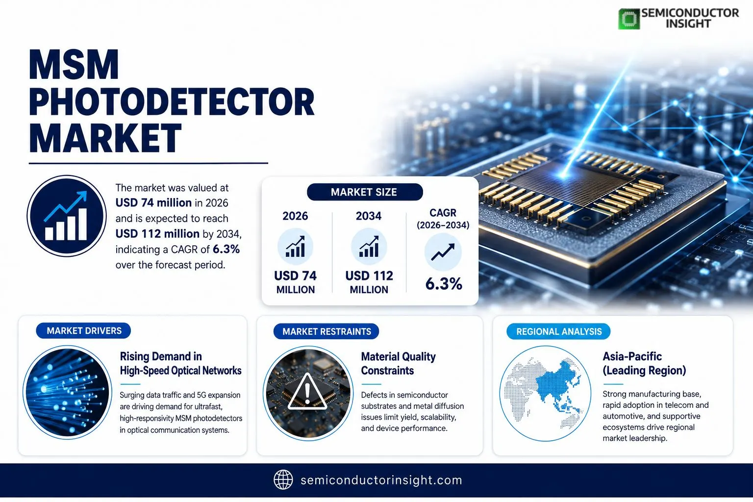
MSM Photodetector market was valued at USD 74 million in 2026 and is expected to reach USD 112 million by 2034, indicating a compound annual growth rate of 6.3% over the forecast period.
A metal‑semiconductor‑metal (MSM) photodetector comprises interdigitated metal fingers fabricated on a semiconductor substrate; it transforms incident photons into electrical signals by collecting photoexcited electrons and holes that drift under the electric field applied between the fingers.The broader semiconductor sector achieved USD 579 billion in revenue during 2022 and is anticipated to climb toward USD 790 billion by 2029, maintaining an approximate six‑percent CAGR. Within this environment, MSM photodetectors underpin key capabilities in optical fiber communications, photonic integrated circuits, and emerging quantum sensing platformsareas that are increasingly demanding higher sensitivity and faster response times.
MARKET DRIVERS
High‑Speed Signal Applications
The push toward gigabit and terabit data rates in optical communication networks fuels demand for ultrafast detection technologies. MSM photodetectors, with sub‑picosecond transit times, are increasingly favored in coherent detection schemes where bandwidth is a linchpin for overall system performance. This speed advantage translates into higher symbol rates, directly boosting network capacity without costly redesign of existing infrastructure.
Integration Readiness
The planar fabrication of MSM structures aligns with silicon CMOS processes, enabling monolithic integration of photodetectors with electronic and photonic circuits. The resulting reduction in parasitic capacitance and improved thermal management enhances reliability and delivery timelines for vendors. Consequently, device yields climb, costs fall, and the economics of deploying large‑area arrays sharpen.
➤ Devices that balance high responsivity with minimal dark current keep the competitive edge in dense photonic chips.
These convergence forces coalesce to make the MSM Photodetector Market a logical destination for companies aiming to shorten time‑to‑market while meeting stringent performance envelopes set by next‑generation data services.
MARKET CHALLENGES
Device Stability Under High‑Power Irradiation
Extended exposure to intense optical fields can erode metal–semiconductor contacts, giving rise to increased series resistance and decreased responsivity. Manufacturers must calibrate bias conditions and employ passivation layers to sustain long‑term operation, which can introduce additional fabrication steps and cost layers.
Other Challenges
Brightness‑Dependent Linear Range
The linear dynamic range of MSM devices shrinks in high‑flux scenarios, limiting their appeal for power‑sensitive sensing applications. Coupled with the need for aggressive biasing to achieve high gain, this presents a delicate trade‑off that product teams are still navigating.
MARKET RESTRAINTS
Material Quality Constraints
Conformity between high‑purity semiconductor substrates and delicate metal contacts remains a persistent hurdle. Defect densities in modern III‑V wafers can cause localized breakdown, while metal diffusion during annealing can shift work function values, ultimately curtailing batch yields. These manufacturing tolerances margin limited scalability for mass‑producible devices.
MARKET OPPORTUNITIES
Edge‑Computing Sensors
The rise of distributed edge‑computing solutions in industrial automation and IoT ecosystems ignites demand for compact, low‑power photodetectors that can harvest weak optical signals. MSM devices, thanks to their planar geometry and robust bias tolerance, are well suited to be embedded within sensor nodes that monitor process variables or perform optical readouts in harsh environments.Cross‑pressures from 5G infrastructure roll‑outs and the proliferation of lidar‑in‑car platforms further amplify opportunities. Automotive lidar scouting projects now rank photodetector selection at the core of cost‑constrained sensor design, where a lightweight and radiation hard device can translate into a critical competitive advantage for original equipment manufacturers.
MSM Photodetector Market Trends
Rising Demand in High‑Speed Optical Networks
With data centers and 5G upgrades worldwide, the throughput demands on optical networks have surged. Companies are deploying denser wavelength‑division multiplexing systems that require photodetectors with rapid rise times and low noise. The market’s expansion is not merely driven by higher data rates but also by the push for energy‑efficient transceivers; MSM photodetectors, offering sub‑nanosecond response and a compact footprint, align seamlessly with these specifications. The cost advantage of MSM devices, especially as interdigitated finger geometry has been refined, improves quantum efficiency while curbing series resistance. The integration of these photodetectors into flexible substrates opens new deployment scenarios such as bendable optical interconnects, thereby extending application boundaries. The semiconductor supply chain adjustments, including a shift toward silicon‑on‑insulator substrates, further reduce material costs, making MSM solutions an attractive choice for OEMs seeking cost leadership.
Other Trends
Photonic Integrated Circuits
Photonic integrated circuits represent a converging path where light and electronics coexist on a single chip. MSM photodetectors are naturally suited to PI systems because their planar architecture dovetails with standard CMOS processes, enabling cost‑effective monolithic integration. Industry surveys indicate that PI system revenues are projected to exceed USD 15 billion by 2026, with the majority of that growth concentrated in data‑center uplinks and edge computing nodes. The agility of MSM devicesfast rise time, high linearity, and low capacitancesupports modulation formats such as PAM‑4 and PRBS used in next‑generation transceivers. Suppliers who can deliver calibrated, high‑yield wafer‑level photodetector arrays are positioned to capture the premium margins associated with PI modules. By 2025, leading vendor integration of lithographic alignment tools has accelerated yield stability, positioning suppliers that invest in precision alignments to secure a foothold in the 5G IMC market.
Automotive LIDAR and Advanced Driver Assistance Systems
Beyond telecom, the automotive sector is ushering a new era of photonics. LIDAR systems and camera‑based advanced driver assistance systems demand sensors that can operate reliably under harsh conditions while delivering millimetre‑level resolution at ranges of 200 meters or higher. MSM photodetectors, with high responsivity at visible to near‑infrared wavelengths and robust packaging, are increasingly chosen for these applications. Vehicle manufacturers are sourcing photodetectors that meet stringent automotive certification standards, driving a steady supply chain path toward high‑volume production. This shift not only diversifies the revenue mix for photodetector producers but also forces a reevaluation of supply‑chain resilience, as the automotive industry prefers in‑region fabrication to mitigate geopolitical risks. Consequently, the MSM Photodetector Market is now being re‑oriented from a primarily telecom focus toward a broader, multi‑occasion ecosystem. Simultaneously, the integration of MSM detectors into hybrid photonics benches for autonomous driving simulations accelerates market penetration, enabling a rapid shift from prototype to production roll‑outs.
COMPETITIVE LANDSCAPEKey Industry Players
MSM Photodetector Market: Competitive Landscape Overview
At the helm of the MSM photodetector ecosystem, Hamamatsu Photonics commands a substantial share of the 74‑million‑dollar market. The Japanese firm leverages its long‑standing laser and detector heritage to offer an integrated portfolio that serves high‑speed optical fiber links, photonic integrated circuits, and emerging artificial‑intelligence accelerators. Recent quarterly revenue growth of 10 % signals resilient demand, while R&D investment has accelerated the transition from conventional GaAs platforms to hybrid silicon‑on‑insulator devices. OSI Laser Diode, meanwhile, has captured a growing niche by standardizing modular MSM modules that enable telecom operators to meet increasing 5G bandwidth requirements without the capital churn of full system redesigns. Together, these two companies operate in a United States‑centric channel network that increasingly incorporates automated test and calibration solutions, thereby locking in customer loyalty through both technology and service integration.Beyond these gatekeepers, a constellation of smaller yet technically sophisticated vendors carve out profitable niches. OSRAM GmbH has focused on automotive‑grade detectors that meet the stringent electromagnetic compatibility and thermal envelope required by advanced driver‑assist systems, while Thorlabs Inc. has excelled in laboratory‑grade instruments that drive rapid prototyping for academic research. Meixner Electronics, PDM Photonics, and Opto‑IX deliver low‑cost, edge‑computing‑oriented MSM modules that fit within the IoT sensor mosaic emphasized by modern microcontroller platforms. Soitec, with its silicon‑on‑insulator foundry capability, is positioned to scale hybrid photonic assemblies, whereas NXP Semiconductors is integrating MSM detectors into its automotive sensor suites. Samsung Advanced Institute contributes through advanced packaging that reduces form‑factor while preserving signal integrity. Instrumentation Corporation and AvTech Photonics diversify the field with consulting‑driven design services and bespoke small‑batch production. This dispersion mitigates concentration risk while fostering cross‑fertilization of innovations, ultimately compelling the market leaders to continually iterate on device efficiency and integration.
List of Key MSM Photodetector Companies Profiled
- Hamamatsu Photonics
- OSI Laser Diode
- Thorlabs Inc.
- OSRAM GmbH
- Meixner Electronics
- PDM Photonics
- Opto-IX
- Soitec
- NXP Semiconductors
- Samsung Advanced Institute
- Instrumentation Corporation
- AvTech Photonics
Segment Analysis:
| Segment Category | Sub-Segments | Key Insights |
| By Type |
|
GaAs-based MSM Photodetectors remain the market leader because of high‑speed detection and extensive integration experience. • Provide low dark current and high quantum efficiency in the visible spectrum. • Compatibility with standard III–V semiconductor fabrication processes reduces cost. • Mature supply chain supports rapid deployment in aerospace and defense systems. • Existing IC libraries enable seamless embedding in photonic integrated circuits. |
| By Application |
|
Optical Fiber Communications handles the bulk of current demand, offering swift response and robust bandwidth. • Essential for ultrafast data links in telecom infrastructure. • Low noise performance ensures signal fidelity over long distances. • Seamless integration with DWDM systems enhances spectral efficiency. • Scalable production aligns with growing bandwidth requirements. |
| By End User |
|
Aerospace & Defense relies heavily on MSM photodetectors for reliable LIDAR and optical ranging. • High radiation tolerance is critical in hostile environments. • Compact form factor supports integration into UAVs and satellites. • Proven longevity reduces maintenance overhead. • Certification compliance ensures adherence to stringent safety standards. |
| By Device Architecture |
|
Waveguide MSM Architecture offers superior coupling efficiency and miniaturisation. • Integrates directly with silicon photonics platforms. • Achieves higher responsivity due to guided mode confinement. • Enables dense integration for sensor arrays. • Facilitates on‑chip signal processing with reduced parasitics. |
| By Cost Category |
|
Low‑Cost Production Segment targets commercial consumer electronics and mass‑market applications. • Utilises cost‑effective deposition techniques and standard wafers. • Scale‑up optimises throughput, driving unit price low. • Maintains sufficient performance for imaging and illumination tasks. • Drives adoption in portable devices and smart cameras. |
Regional Analysis: MSM Photodetector Market
North America
Deep‑level defect control, process uniformity, and packaging reliability define the competitive landscape, pushing manufacturers toward advanced CVD methods that ensure stable bias drift and high dynamic range in vertical‑stacked photodetectors.
Joint ventures between semiconductor giants and start‑up photonic firms enable knowledge transfer, accelerate test bed deployment, and secure early market penetration for niche sensing solutions.
Growth in autonomous navigation, precision agriculture, and homeland‑security imaging fuels demand for low‑noise, high‑sensitivity assemblies that can operate under extreme illumination conditions.
Capital allocations are increasingly earmarked for R&D in silicon‑on‑insulator platforms, with investors favoring pitches that promise scalable manufacturing and lower per‑unit cost trajectories.
Europe
The European market is pivoting toward the convergence of photonic sensing and quantum communication infrastructures. Material quality standards and governmental standards around electromagnetic compatibility push firms to refine device architecture. Rising demand in medical imaging and satellite remote sensing commits manufacturers to stricter noise tolerance and radiation hardness. Although higher regulatory overhead slows deployment, it also filters out competitors, allowing firms that comply to secure long‑term contracts with defense and space agencies. Enhanced academic collaboration channels talent into centered research hubs, fostering a pipeline of certifications that feed into industry supply chains tailored for high‑precision instrumentation.
Asia-Pacific
In the Asia‑Pacific corridor, a vibrant ecosystem of specialty light‑source makers and integrated photonics labs accelerates prototyping cycles. The region leverages low‑cost fabrication facilities and a growing network of venture capital that favors early‑stage sensor start‑ups. Consumer electronics and automotive lidar segments demand robust, low‑cost photodetectors that maintain performance across temperature swings. Local supply chains are adapting to accommodate high‑throughput assembly lines, balancing yield improvement with cost containment. A noticeable trend is the partnership between chip manufacturers and optical subsystem integrators, which streamlines design validation and accelerates product rollouts into fast‑growing markets for smart cities and autonomous transport.
South America
South America’s rise hinges on the adoption of photonic sensors within the agritech and environmental monitoring sectors. Policy incentives aimed at precision farming create new revenue streams for detectors that can track crop health, soil moisture, and atmospheric conditions. Meanwhile, national space agencies are commissioning low‑cost, high‑resolution imaging satellites, driving demand for miniaturized, radiation‑tolerant photodetectors. While the logistical footprint is modest, firms that formulate a lean supply chain and focus on niche applicationssuch as greenhouse monitoringcan secure a foothold before competition intensifies.
Middle East & Africa
The Middle East and Africa region is shaping its MSM Photodetector Market around infrastructure resilience and security‑centric applications. Urban sensing for water and power grid optimization requires detectors with long‑term reliability and low power consumption. Governments prioritize domestic manufacturing capacity to reduce dependency on foreign suppliers. This push has encouraged joint development agreements between local conglomerates and foreign photonics leaders, fostering technology transfer while ensuring compliance with stringent safety and environmental regulations. In the security domain, the need for night‑time imaging devices that operate in harsh coastal climates drives focused niche development, positioning regional manufacturers as specialized players in high‑value defense contracts.
{/html}
Report Scope
This market research report provides a comprehensive analysis of the MSM Photodetector Market , covering the forecast period 2026–2034. It offers detailed insights into market dynamics, technological advancements, competitive landscape, and key trends shaping the industry.
Key focus areas of the report include:
- Market Overview: The report begins with an overview outlining its current market scenario, key growth indicators, and industry transformation drivers. It discusses macroeconomic factors, demand–supply balance, regulatory landscape, and the strategic role of semiconductors in powering advancements across industries such as automotive, telecommunications, consumer electronics, and industrial automation.
- Market Size & Forecast: Historical data and future projections for revenue, unit shipments, and market value across major regions and segments.
- Segmentation Analysis: Detailed breakdown by product type, technology, application, and end-user industry to identify high-growth segments and investment opportunities.
- Regional Insights: Insights into market performance across North America, Europe, Asia-Pacific, Latin America, and the Middle East & Africa, including country-level analysis where relevant.
- Competitive Landscape: Profiles of leading market participants, including their product offerings, R&D focus, manufacturing capacity, pricing strategies, and recent developments such as mergers, acquisitions, and partnerships.
- Technology Trends & Innovation: Assessment of emerging technologies, integration of AI/IoT, semiconductor design trends, fabrication techniques, and evolving industry standards.
- Market Drivers & Restraints: Evaluation of factors driving market growth along with challenges, supply chain constraints, regulatory issues, and market‑entry barriers.
- Stakeholder Insights: Insights for component suppliers, OEMs, system integrators, investors, and policymakers regarding the evolving ecosystem and strategic opportunities.
Primary and secondary research methods are employed, including interviews with industry experts, data from verified sources, and real‑time market intelligence to ensure the accuracy and reliability of the insights presented.
FREQUENTLY ASKED QUESTIONS:
What is the current market size of MSM Photodetector Market?
-> MSM Photodetector market was valued at USD 74 million in 2026 and is projected to reach USD 112 million by 2034, at a CAGR of 6.3% during the forecast period.
Which key companies operate in MSM Photodetector Market?
-> Key players include Hamamatsu Photonics and OSI Laser Diode.
What are the key growth drivers?
-> Driving forces include the growing demand for optical communication systems, the expansion of photonic integrated circuits, and the increasing adoption of MSM photodetectors in automotive and industrial automation applications.
Which region dominates the market?
-> Asia‑Pacific leads the MSM Photodetector market, supported by rapid adoption across telecommunications and automotive sectors.
What are the emerging trends?
-> Emerging trends encompass the integration of MSM photodetectors in fiber‑optic communication networks, advancements in photonic integrated circuitry, and the development of high‑speed, low‑power detection technologies.

Get Sample Report PDF for Exclusive Insights
Report Sample Includes
- Table of Contents
- List of Tables & Figures
- Charts, Research Methodology, and more...
 Download Sample Report PDF




