
Molybdenum (Mo) Contact Layer Market Insights
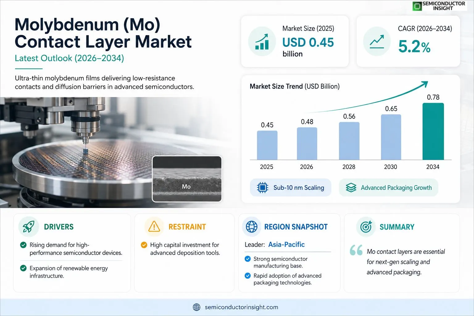
Global Molybdenum (Mo) contact layer market size was valued at USD 0.45 billion in 2025. The market is projected to grow from USD 0.48 billion in 2026 to USD 0.78 billion by 2034, exhibiting a CAGR of 5.2% during the forecast period.
Molybdenum contact layers are ultra‑thin metallic films deposited on semiconductor wafers to provide low‑resistance electrical pathways and robust diffusion barriers in advanced logic and memory devices. Their high melting point, excellent conductivity, and compatibility with copper interconnects make them essential for sub‑10 nm technology nodes.The market is accelerating because semiconductor manufacturers are scaling down device dimensions while demanding higher performance and reliability. Furthermore, increased capital spending on advanced packaging, such as chip‑on‑wafer‑stack (CoWS) and heterogeneous integration, fuels demand for Mo contact solutions. Key players,including Applied Materials, Lam Research, Tokyo Electron, and Hitachi High‑Technologies,are expanding their process portfolios and investing in next‑generation deposition equipment to capture this growth.
MARKET DRIVERS
Growing Demand for High‑Performance Semiconductor Devices
Molybdenum (Mo) Contact Layer Market is being propelled by the surge in advanced semiconductor applications, where Mo’s superior thermal stability and low resistivity enable finer line widths and higher current densities. Manufacturers are increasingly adopting Mo contact layers to meet the performance targets of 7‑nm and sub‑7‑nm technology nodes.
Expansion of Renewable Energy Infrastructure
Renewable energy systems, especially photovoltaic and wind turbine converters, rely on Mo‑based contact layers for their durability under harsh environmental conditions. This sector’s rapid growth contributes significantly to the overall volume of Mo contact layer consumption.
➤ Strategic partnerships between Mo suppliers and silicon foundries are accelerating material qualification cycles, shortening time‑to‑market for next‑generation chips.
In addition, government incentives for low‑carbon technologies are fostering investments in equipment that leverage Mo contact layers, further strengthening market momentum.
MARKET CHALLENGES
Integration Complexity with Existing Process Flows
Adopting Mo contact layers often requires re‑engineering of deposition and etching steps. Legacy fabs face steep learning curves and capital expenditures to retrofit equipment, which can delay implementation timelines.
Other Challenges
Material Purity and Yield Consistency
Achieving ultra‑high purity Mo films is critical to avoid contamination that could compromise device reliability. Variability in film uniformity remains a concern for high‑volume production.
MARKET RESTRAINTS
High Capital Investment for Advanced Deposition Tools
The required specialized sputtering and atomic layer deposition (ALD) systems for Mo contact layers involve substantial upfront costs. Small‑ to mid‑size fabs may defer adoption until equipment prices decrease or financing options improve, limiting short‑term market expansion.
MARKET OPPORTUNITIES
Emergence of 3D‑IC and Heterogeneous Integration
3D‑IC architectures demand reliable vertical interconnects, where Mo contact layers excel due to their excellent adhesion and low electromigration rates. This creates a sizable growth avenue for suppliers capable of delivering high‑quality, thin‑film Mo solutions tailored for stacked‑die configurations.
Molybdenum (Mo) Contact Layer Market Trends
Scaling Demand for Ultra‑Thin Mo Contact Layers
The market for Molybdenum (Mo) contact layers is expanding as semiconductor manufacturers target sub‑10 nm technology nodes. At these dimensions, the electrical resistance of interconnects becomes a limiting factor, and Mo’s low‑resistivity, high melting point, and compatibility with copper enable the creation of ultra‑thin diffusion barriers that maintain signal integrity. Process engineers are increasingly adopting atomic‑layer‑deposition (ALD) and advanced chemical‑vapor‑deposition (CVD) techniques to achieve the uniform film thickness required for next‑generation logic and memory chips. This shift is reinforced by the broader industry focus on power efficiency and higher transistor density, which together elevate the strategic importance of Mo contact solutions across the front‑end manufacturing flow. Additionally, the transition to low‑k dielectric materials intensifies the need for robust barrier layers that prevent copper migration, further cementing Mo’s role in achieving reliable device performance.
Other Trends
Advanced Packaging Integration
CoWS and heterogeneous integration represent a new wave of three‑dimensional packaging that stacks multiple functional blocks within a single package. These architectures demand high‑density interconnects with minimal parasitic effects, driving demand for Mo contact layers that can be applied to both die‑level and wafer‑level bonding processes. The material’s ability to form continuous, pinhole‑free films at nanometer scale makes it ideal for ensuring mechanical stability and electrical continuity across stacked dies. Moreover, Mo’s resistance to electromigration supports the long‑term reliability targets required for high‑performance computing and automotive applications, encouraging OEMs to specify Mo barriers in their advanced packaging roadmaps.
Equipment Expansion by Key Suppliers
Major equipment manufacturers are responding by broadening their Mo deposition portfolios. Applied Materials and Lam Research have introduced ALD modules that deliver sub‑nanometer thickness control, while Tokyo Electron and Hitachi High‑Technologies are upgrading their CVD platforms to accommodate higher throughput without compromising film uniformity. These investments include enhanced process monitoring, in‑situ metrology, and automated recipe management, which together reduce cycle time and improve yield for high‑volume production. As fabs integrate these advanced tools, the overall adoption of Mo contact layers is expected to accelerate, reinforcing the market’s upward trajectory and solidifying Mo as a cornerstone material in the evolving semiconductor ecosystem.
COMPETITIVE LANDSCAPEKey Industry Players
Molybdenum (Mo) Contact Layer Market: Competitive Dynamics and Growth Drivers
Applied Materials dominates the Mo contact layer segment through its advanced physical vapor deposition (PVD) and atomic layer deposition (ALD) platforms, leveraging a broad installed base in leading fabs and capitalizing on the market’s valuation of USD 0.45 billion in 2025 with a projected CAGR of 5.2 % to 2034. Lam Research and Tokyo Electron reinforce the competitive structure with complementary etch, clean and deposition solutions that enable sub‑10 nm node performance. These three firms collectively control the majority of equipment spend, driving the industry toward higher throughput, lower defectivity, and tighter integration with copper interconnects. Their strategic investments in next‑generation deposition heads, high‑k dielectric compatibility, and collaborative R&D with chipmakers such as Intel and Samsung are central to sustaining the growth trajectory from USD 0.48 billion in 2026 to an estimated USD 0.78 billion by 2034.In addition to the primary equipment leaders, a cohort of niche specialists adds depth to the ecosystem. Hitachi High‑Technologies and KLA Corp provide precision metrology and inspection tools essential for ensuring Mo film uniformity, while JSR Corporation and ASM International deliver specialized chemical vapor deposition (CVD) and ALD precursors that enhance barrier performance. Veeco Instruments and Picosun Ltd. focus on plasma‑enhanced ALD for ultra‑thin layers, supporting advanced packaging formats such as chip‑on‑wafer‑stack (CoWS). Regional contributors like Shanghai Micro Electronics (SMEE) and Taiwan’s TSMC (through in‑house process development) expand the supply chain in Asia, and major semiconductor designers,Intel, Samsung Electronics, and Advanced Micro Devices (AMD),drive demand through their own fab expansions and heterogeneous integration programs. This diversified mix of equipment, materials, and end‑user expertise creates a resilient competitive landscape that is poised to meet the accelerating requirements of next‑generation logic and memory devices.
List of Key Molybdenum (Mo) Contact Layer Companies Profiled
- Applied Materials
- Lam Research
- Tokyo Electron
- Hitachi High‑Technologies
- KLA Corp
- JSR Corporation
- Veeco Instruments
- ASM International
- SMEE (Shanghai Micro Electronics)
- TSMC (Taiwan Semiconductor Manufacturing Co.)
- Intel Corporation
- Samsung Electronics
- Picosun Ltd.
- NovaIntegrated
- Advanced Micro Devices (AMD)
Segment Analysis:
| Segment Category | Sub-Segments | Key Insights |
| By Type |
|
Pure molybdenum continues to dominate due to its intrinsic high melting point and excellent conductivity.
Alloyed variants are gaining traction where enhanced mechanical strength or tailored stress gradients are needed, especially in high‑density stacking scenarios. Composite stacks combine barrier and adhesion functions, streamlining process steps and reducing overall wafer handling. |
| By Application |
|
Advanced logic drives molecular‑level precision in contact layer engineering.
Memory applications value the barrier reliability of Mo to protect dense stack layers, and 3D packaging relies on its thin‑film uniformity to maintain alignment across multiple die tiers. |
| By End User |
|
IDMs prioritize process consistency and long‑term material reliability, making Mo contact layers a strategic choice for in‑house product roadmaps.
Foundries emphasize flexibility, providing a portfolio of Mo options that can be tuned to diverse customer designs, while OEMs in packaging look for thin, robust barriers to support heterogeneous integration. |
| By Process Technology |
|
Sub‑nanometer nodes require contact layers that remain conductive and stable at extreme aspect ratios.
The synergy between Mo and GAA designs is highlighted by the material’s ability to act as both barrier and contact without compromising device scaling ambitions. |
| By Market Driver |
|
Performance scaling is the core catalyst, pushing designers to seek materials that sustain high‑frequency operation while limiting RC delay.
The combined pressure of reliability expectations and packaging innovation reinforces Mo’s strategic position within the semiconductor ecosystem. |
Regional Analysis: North America
United States
The aerospace and defense industries are major consumers of Molybdenum (Mo) Contact Layer due to its high-temperature resistance and electrical conductivity. Strict reliability requirements and demanding operational conditions necessitate the use of premium contact layer materials. Growth in military spending and the development of advanced aerospace technologies are driving demand in this segment.
The semiconductor packaging industry relies heavily on Molybdenum (Mo) Contact Layer for efficient heat dissipation and reliable electrical connections. Miniaturization of electronic devices and increasing power densities are driving the demand for advanced contact layer materials with superior thermal conductivity. Research into new packaging technologies, such as 2.5D and 3D integration, is creating further opportunities.
Industrial electronics applications, including power electronics and motor control systems, utilize Molybdenum (Mo) Contact Layer for its robust performance and reliability. Increasing adoption of electric vehicles and renewable energy technologies is contributing to the growth of this segment. The demand for high-power and high-frequency applications is driving innovation in contact layer materials.
Medical devices often require reliable and biocompatible contact layers, leading to applications of Molybdenum (Mo) Contact Layer in certain specialized devices. The stringent regulatory requirements and safety standards in the medical device industry influence the selection of materials.
Europe
Europe presents a stable market for Molybdenum (Mo) Contact Layer, with key demand originating from the automotive, aerospace, and industrial sectors. The region is characterized by a strong focus on sustainability and energy efficiency, influencing the development of advanced materials for various applications. The automotive industry’s transition towards electric vehicles is creating both opportunities and challenges for Molybdenum (Mo) Contact Layer Market. Stringent environmental regulations and a commitment to circular economy principles are shaping the materials landscape. Research and development activities are focused on improving the performance and durability of contact layers while minimizing environmental impact. The European market is highly competitive, with a strong presence of established manufacturers and emerging players. The demand for high-performance Molybdenum (Mo) Contact Layer in aerospace applications remains robust, while the industrial sector is driving growth in specific segments. Moreover, the increasing adoption of advanced packaging technologies in the electronics industry is contributing to market expansion.
Asia-Pacific
Asia-Pacific is the fastest-growing market for Molybdenum (Mo) Contact Layer, driven by rapid industrialization, increasing electronics manufacturing, and strong investments in infrastructure. China, Japan, South Korea, and Taiwan are key contributors to this growth. The region’s robust semiconductor industry is a major driver of demand, with significant investments in advanced packaging and chip manufacturing facilities. Government initiatives promoting domestic chip production and technological self-sufficiency are further fueling market expansion. The automotive industry in Asia-Pacific is also experiencing rapid growth, leading to increased demand for contact layers in electric vehicle components. The increasing adoption of 5G technologies and the growth of the Internet of Things (IoT) are creating new opportunities for Molybdenum (Mo) Contact Layer. However, the market in Asia-Pacific is also characterized by intense competition and price sensitivity. The regulatory landscape varies across different countries in the region, presenting both opportunities and challenges for manufacturers. There is a growing emphasis on local manufacturing and supply chain resilience, which is influencing investment decisions.
South America
South America represents a relatively smaller but growing market for Molybdenum (Mo) Contact Layer. The industrial sector, particularly in Brazil and Argentina, is the primary driver of demand. The mining and metals industries contribute significantly to the market, requiring contact layers for various applications. The automotive sector is also experiencing growth, albeit at a slower pace compared to other regions. Increased investments in infrastructure projects are expected to boost demand in the coming years. The market in South America is characterized by a limited number of suppliers and a greater reliance on imports. The regulatory environment can be complex, and political and economic uncertainties can impact market growth. There is potential for growth in specific niche applications, such as specialized industrial equipment and renewable energy systems.
Middle East & Africa
The Middle East & Africa market for Molybdenum (Mo) Contact Layer is emerging, with growth driven by increasing investments in infrastructure, industrial development, and the oil & gas sector. The oil and gas industry requires robust contact layers for downhole tools and equipment. The construction sector, particularly in countries like Saudi Arabia and the UAE, is driving demand for materials used in power transmission and distribution systems. The automotive industry is also growing, contributing to demand in specific applications. Government initiatives promoting economic diversification and industrialization are expected to fuel further market expansion. The market is characterized by a relatively small number of established players, and there is potential for growth for companies that can offer customized solutions and reliable supply chains. The regulatory environment varies across different countries in the region, and political factors can influence market dynamics.
Report Scope
This market research report provides a comprehensive analysis of the Molybdenum (Mo) Contact Layer Market , covering the forecast period 2026–2034. It offers detailed insights into market dynamics, technological advancements, competitive landscape, and key trends shaping the industry.
Key focus areas of the report include:
- Market Overview: The report begins with an overview outlining its current market scenario, key growth indicators, and industry transformation drivers. It discusses macroeconomic factors, demand–supply balance, regulatory landscape, and the strategic role of semiconductors in powering advancements across industries such as automotive, telecommunications, consumer electronics, and industrial automation.
- Market Size & Forecast: Historical data and future projections for revenue, unit shipments, and market value across major regions and segments.
- Segmentation Analysis: Detailed breakdown by product type, technology, application, and end-user industry to identify high-growth segments and investment opportunities.
- Regional Insights: Insights into market performance across North America, Europe, Asia-Pacific, Latin America, and the Middle East & Africa, including country-level analysis where relevant.
- Competitive Landscape: Profiles of leading market participants, including their product offerings, R&D focus, manufacturing capacity, pricing strategies, and recent developments such as mergers, acquisitions, and partnerships.
- Technology Trends & Innovation: Assessment of emerging technologies, integration of AI/IoT, semiconductor design trends, fabrication techniques, and evolving industry standards.
- Market Drivers & Restraints: Evaluation of factors driving market growth along with challenges, supply chain constraints, regulatory issues, and market-entry barriers.
- Stakeholder Insights: Insights for component suppliers, OEMs, system integrators, investors, and policymakers regarding the evolving ecosystem and strategic opportunities.
Primary and secondary research methods are employed, including interviews with industry experts, data from verified sources, and real-time market intelligence to ensure the accuracy and reliability of the insights presented.
FREQUENTLY ASKED QUESTIONS:
What is the current market size of Molybdenum (Mo) Contact Layer Market?
-> Molybdenum (Mo) Contact Layer Market was valued at USD 0.45 billion in 2025 and is expected to reach USD 0.78 billion by 2034, reflecting a CAGR of 5.2% over the forecast period.
Which key companies operate in Molybdenum (Mo) Contact Layer Market?
-> Key players include Applied Materials, Lam Research, Tokyo Electron, and Hitachi High‑Technologies, among others.
What are the key growth drivers?
-> Key growth drivers include scaling down device dimensions, demand for higher performance and reliability, and increased capital spending on advanced packaging such as chip‑on‑wafer‑stack (CoWS) and heterogeneous integration.
Which region dominates the market?
-> The reference does not specify a dominant region.
What are the emerging trends?
-> Emerging trends include advanced packaging techniques like CoWS and heterogeneous integration, as well as the development of ultra‑thin Mo contact layers for sub‑10 nm technology nodes.

Get Sample Report PDF for Exclusive Insights
Report Sample Includes
- Table of Contents
- List of Tables & Figures
- Charts, Research Methodology, and more...
 Download Sample Report PDF


