
Laser Assisted Bonding (LAB) Market Insights
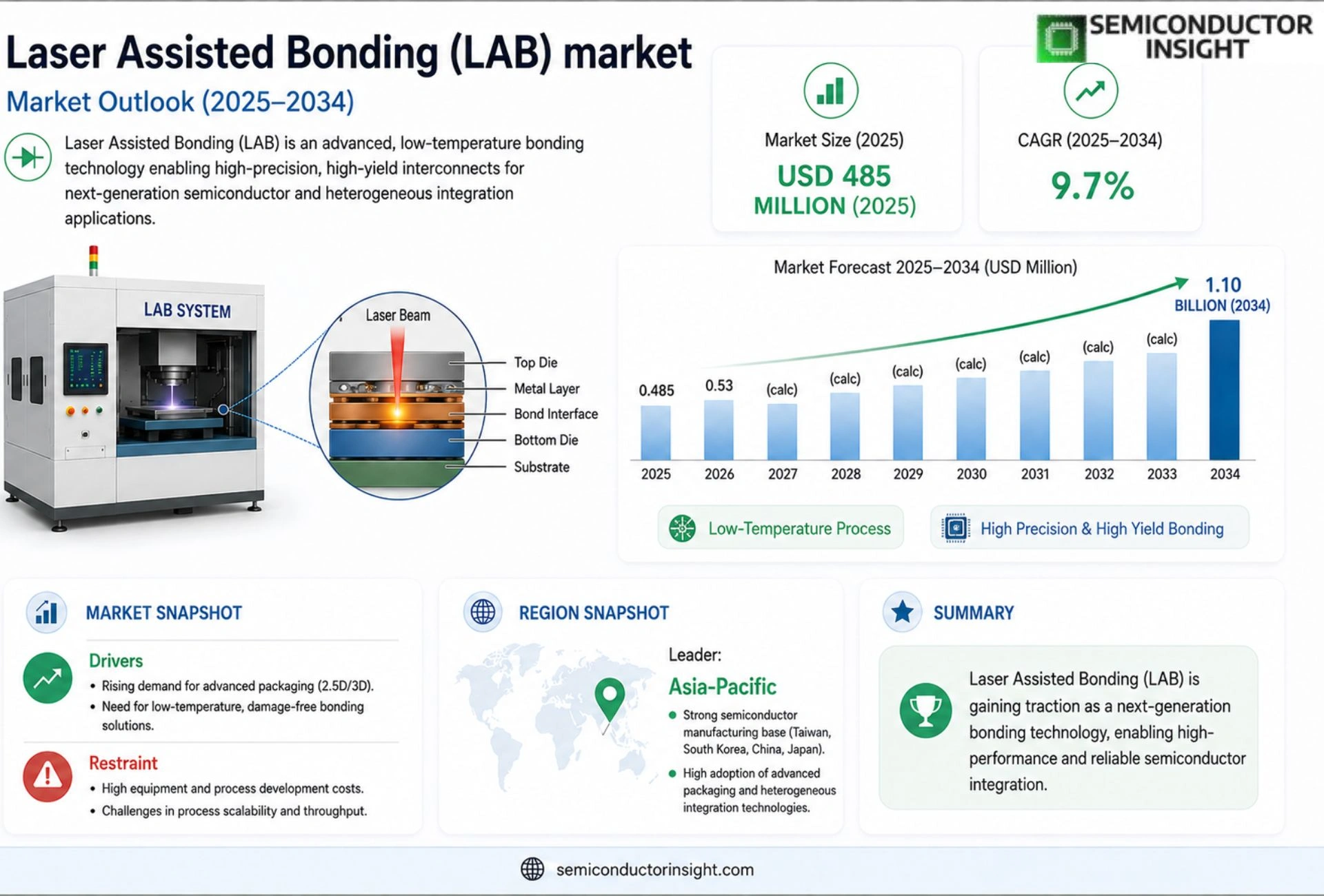
Global Laser Assisted Bonding (LAB) market size was valued at USD 485 million in 2025. The market is projected to grow from USD 530 million in 2026 to USD 1.1 billion by 2034, exhibiting a CAGR of 9.7% during the forecast period.
Laser Assisted Bonding (LAB) is an advanced semiconductor packaging technology that utilizes laser energy to form precise, high-strength bonds between dissimilar materials, such as silicon dies and substrates. This process enhances thermal management, electrical performance, and mechanical reliability in microelectronic devices, making it particularly valuable for applications in automotive electronics, aerospace systems, and high-performance computing. LAB eliminates traditional limitations associated with conventional bonding methods,such as thermal stress and misalignment,by enabling localized heating with minimal heat-affected zones. Furthermore, the technology supports heterogeneous integration, allowing manufacturers to combine different materials like copper, aluminum nitride (AlN), and silicon carbide (SiC) without compromising structural integrity.
MARKET DRIVERS
Expanding Microelectronics Industry Demands
The global push for smaller, more powerful devices significantly drives Laser Assisted Bonding (LAB) Market. As semiconductor manufacturers strive for higher integration levels, non-destructive bonding techniques become essential for maintaining device integrity without compromising performance. This trend is particularly evident in the production of complex integrated circuits where precise material joining is critical.
Increasing Adoption in 3D Packaging
Advanced packaging technologies, such as Through-Silicon Vias (TSVs) and heterogeneous integration, are creating new avenues for growth withLaser Assisted Bonding (LAB) Market. These technologies allow for vertical stacking and improved signal integrity, requiring robust bonding solutions that can operate at micron-level precision and low thermal impact, which LAB provides effectively.
➤ Growth in demand for non-contact processes to mitigate thermal stress and damage to sensitive substrates.
Furthermore, the trend towards automation in manufacturing facilities has increased the demand for high-throughput laser bonding systems, making automated processes a key factor in market expansion strategies.
MARKET CHALLENGES
Sensitivity to Material Variability
Laser Assisted Bonding (LAB) Market faces hurdles due to the sensitivity of the technology to variations in material properties. Different substrates, such as silicon, glass, and copper alloys, require specific laser parameters, including wavelength and energy density. This variability complicates production lines and necessitates rigorous quality control processes to prevent bonding defects that are difficult to detect after the process is complete.
Other Challenges
High Initial Capital Expenditure
Industrial-grade laser systems required for LAB operations represent a substantial financial burden for manufacturers, particularly small and medium-sized enterprises looking to upgrade their facilities.
MARKET RESTRAINTS
Regulatory Compliance and Safety Standards
Strict government regulations regarding occupational safety and laser radiation pose significant restraints to market expansion. Operating high-power lasers requires specialized protective enclosures and personnel training, which adds operational complexity and cost. Manufacturers must navigate a complex landscape of international standards to ensure that their operations remain compliant, slowing down the adoption of LAB technology in emerging markets.
MARKET OPPORTUNITIES
Expansion in Automotive Sector Applications
The rapid electrification of vehicles offers significant opportunities for Laser Assisted Bonding (LAB) Market. Modern electric vehicles rely on sophisticated sensing systems, power electronics, and advanced driver-assistance systems (ADAS). The reliability and precision required for manufacturing these critical components make laser bonding an ideal technology for high-volume automotive electronics production, driving investment in this sector.
Additionally, the growing consumer demand for wearable technology and medical implants presents a high-growth niche for miniaturized bonding solutions that offer superior biocompatibility and durability.
Trends
Primary Trend Heading Here
Laser Assisted Bonding (LAB) is emerging as a crucial technology in semiconductor packaging, addressing the increasing demands for miniaturization and enhanced performance in electronic devices. The application of laser energy to create strong, precise bonds between diverse materials is driving significant advancements in the industry. This technology facilitates the integration of various materials like silicon, copper, and silicon carbide, which were previously challenging to combine effectively. The rise of automotive electronics, aerospace systems, and high-performance computing are key drivers for the growing adoption of Laser Assisted Bonding (LAB).
Other Trends
Advanced Materials Integration
One of the most prominent trends is the increasing integration of advanced materials using LAB. Copper and silicon carbide are gaining traction as alternatives to traditional materials, offering improved thermal conductivity and power handling capabilities. This integration is critical for next-generation electronic components requiring higher efficiency and reliability. The ability of LAS to create strong bonds between these materials without compromising performance is a substantial advantage.
Enhanced Thermal Management
The demand for better thermal management solutions is a significant trend Laser Assisted Bonding (LAB) Market. By enabling efficient heat dissipation, LAB contributes to improved device reliability and performance. This is particularly important in high-power applications such as electric vehicles and data centers where heat generation is a major concern.
Heterogeneous Integration Advancements
Heterogeneous integration, which involves combining different types of chips and components on a single package, is another crucial trend. LAB plays a vital role in this process by providing a reliable and precise method for bonding dissimilar materials. This facilitates the creation of more complex and powerful electronic systems in a smaller form factor.
The increasing complexity of electronic devices is fueling the demand for sophisticated packaging technologies. Laser Assisted Bonding (LAB) is well-positioned to meet these evolving needs, offering a versatile and reliable solution for bonding dissimilar materials. As the market continues to expand, further innovation in LAB technology is expected to unlock new possibilities and drive advancements across various industries.
Improved Reliability and Performance
Laser Assisted Bonding (LAB) significantly improves the reliability and performance of electronic devices. Compared to traditional bonding methods, LAB minimizes thermal stress and misalignment, leading to more robust and dependable products. This is reflected in its growing adoption across critical applications requiring high levels of performance and longevity.
COMPETITIVE LANDSCAPE
Key Industry Players
Laser Assisted Bonding (LAB) Market Analysis
Laser Assisted Bonding (LAB) Market is experiencing significant growth, projected to reach USD 1.1 billion by 2034 with a CAGR of 9.7%. This growth is fueled by increasing demand for advanced semiconductor packaging solutions that enhance thermal management and reliability in demanding applications. Key players in this market are focused on developing innovative LAB technologies to address the challenges of heterogeneous integration and miniaturization in microelectronic devices. The market’s expansion is particularly driven by the automotive electronics, aerospace, and high-performance computing sectors, all requiring higher levels of performance and reliability.
Several companies are actively involved in the LAB market, offering both equipment and services. These include established semiconductor equipment manufacturers and specialized laser technology providers. The competitive landscape is characterized by ongoing research and development efforts aimed at improving the precision, speed, and cost-effectiveness of LAB processes. Strategic partnerships and collaborations are also prevalent, enabling companies to expand their technological capabilities and market reach. The demand for LAB is directly correlated with the increasing complexity of integrated circuits and the need for advanced packaging techniques.
List of Key Laser Market Companies Profiled
- Amada Toho Machine Tool, Ltd.
- Fanuc Corporation
- Trumpf AG
- Coherent, Inc.
- IPG Photonics Corporation
- Universal Laser Systems
- Han’s Laser Technology Co., Ltd.
- Nagase Electronics Co., Ltd.
- Mitsubishi Electric Corporation
- KYOWA KOGAKU K.K.
- Lasertec Corporation
- Rofin-Sinar Laser GmbH
- Prima Laser Systems
Segment Analysis:
| Segment Category | Sub-Segments | Key Insights |
| By Type |
|
Leading Segment description with qualitative insights only [Pointers preferred in bullets atleast 2-3]. The market sees strong adoption of wafer-level bonding for high-frequency applications, driven by its ability to enhance performance and reduce size. Package-level bonding remains crucial for mainstream applications, focusing on cost-effectiveness and reliability. Die-to-wafer bonding is gaining traction for advanced packaging needs, particularly in high-performance computing. |
| By Application |
|
Leading Segment description with qualitative insights only [Pointers preferred in bullets atleast 2-3]. Automotive electronics is a significant driver, requiring robust and reliable bonding for various sensors and control units. Aerospace and defense benefits from LAB’s ability to create lightweight and high-performance components. High-performance computing demands advanced bonding solutions for efficient heat dissipation and signal integrity. Consumer electronics utilizes LAB for miniaturization and enhanced functionality. |
| By End User |
|
Leading Segment description with qualitative insights only [Pointers preferred in bullets atleast 2-3]. Semiconductor manufacturers are key adopters to improve chip performance and reliability. LED manufacturers leverage LAB for efficient thermal management and compact designs. Microcontroller manufacturers find LAB beneficial for integrating multiple functionalities into smaller packages. |
| By Material Combination |
|
Leading Segment description with qualitative insights only [Pointers preferred in bullets atleast 2-3]. Silicon to silicon bonding is a foundational technique, focusing on achieving high electrical performance. Silicon to copper bonding is gaining popularity for improving thermal conductivity in high-power devices. Silicon to aluminum bonding offers a cost-effective solution for various packaging applications. |
| By Node Size |
|
Leading Segment description with qualitative insights only [Pointers preferred in bullets atleast 2-3]. The 28nm and above node size segment represents the mature market, focusing on cost-optimized solutions. The 16nm segment is experiencing growth due to its balance of performance and power efficiency. The 10nm and below segments are driving innovation, demanding advanced bonding techniques for miniaturization and higher performance. |
Regional Analysis:
LAB is increasingly utilized in the aerospace sector for joining dissimilar materials, reducing weight, and enhancing structural integrity in aircraft components. This technology enables the creation of more fuel-efficient and durable aircraft.
The automotive industry is adopting LAB for joining aluminum and other lightweight materials, contributing to improved fuel economy and reduced emissions. The demand for stronger and more reliable bonds in automotive applications is driving LAB adoption.
LAB plays a critical role in the electronics and semiconductor industries for precise and reliable joining of components with varying thermal expansion coefficients. The miniaturization of electronic devices is further fueling the demand for advanced joining techniques like LAB.
The medical device industry leverages LAB for creating biocompatible and durable bonds in implants and surgical instruments. The precision and control offered by LAB are essential for medical device manufacturing.
Europe
Europe is witnessing steady growth Laser Assisted Bonding (LAB) Market. Driven by a strong emphasis on sustainability and advanced manufacturing, the region presents a significant opportunity for LAB technology. Several European countries, particularly Germany and the UK, are investing heavily in R&D related to advanced joining techniques. The automotive and aerospace sectors in Europe are key consumers of LAB, seeking solutions for lightweighting and improved material performance. Government initiatives promoting industrial modernization and technological advancement are further supporting the market’s expansion. The focus on circular economy principles also encourages the adoption of efficient joining processes like LAB, minimizing material waste. Furthermore, collaborations between academic institutions and industry players are fostering innovation in LAB applications.
Asia-Pacific
The Asia-Pacific region is emerging as a rapidly growing market for Laser Assisted Bonding (LAB). Fueled by robust industrialization, particularly in countries like China and Japan, the demand for advanced joining technologies is soaring. The electronics manufacturing sector in Asia-Pacific is a major driver of LAB adoption, requiring precise and reliable bonding solutions for intricate components. The automotive industry in the region is also increasingly utilizing LAB for lightweighting and improving fuel efficiency. Government support for advanced manufacturing and technological innovation is a key factor contributing to the market’s growth. The expanding aerospace industry in countries like India and South Korea is also creating new opportunities for LAB applications. The cost-effectiveness and efficiency of LAB processes are attractive to manufacturers in the region.
South America
South America represents a nascent but promising market for Laser Assisted Bonding (LAB). The region’s growing automotive and aerospace industries are expected to drive demand for this advanced joining technology. Increased investments in manufacturing infrastructure and a growing focus on technological upgrades are facilitating LAB adoption. However, the market is currently constrained by factors such as higher initial investment costs and a limited awareness of LAB’s potential. Government policies supporting industrial development and technological innovation are crucial for fostering market growth in South America. The potential for LAB to enhance the competitiveness of regional industries presents a significant opportunity.
Middle East & Africa
The Middle East & Africa region presents a relatively untapped market for Laser Assisted Bonding (LAB). The burgeoning aerospace and automotive sectors in countries like the UAE and South Africa are expected to create demand for this technology. Increased investments in infrastructure development and a growing focus on diversification away from traditional oil-based economies are driving industrial growth in the region. However, the market is currently limited by factors such as a lack of skilled labor and limited awareness of LAB’s capabilities. Government initiatives promoting industrialization and technological advancement are essential for fostering market growth. The potential for LAB to enhance the efficiency and competitiveness of regional industries presents a significant long-term opportunity.
Report Scope
This market research report provides a comprehensive analysis of the Laser Assisted Bonding (LAB) Market , covering the forecast period 2026–2034. It offers detailed insights into market dynamics, technological advancements, competitive landscape, and key trends shaping the industry.
Key focus areas of the report include:
- Market Overview: The report begins with an overview outlining its current market scenario, key growth indicators, and industry transformation drivers. It discusses macroeconomic factors, demand–supply balance, regulatory landscape, and the strategic role of semiconductors in powering advancements across industries such as automotive, telecommunications, consumer electronics, and industrial automation.
- Market Size & Forecast: Historical data and future projections for revenue, unit shipments, and market value across major regions and segments.
- Segmentation Analysis: Detailed breakdown by product type, technology, application, and end-user industry to identify high-growth segments and investment opportunities.
- Regional Insights: Insights into market performance across North America, Europe, Asia-Pacific, Latin America, and the Middle East & Africa, including country-level analysis where relevant.
- Competitive Landscape: Profiles of leading market participants, including their product offerings, R&D focus, manufacturing capacity, pricing strategies, and recent developments such as mergers, acquisitions, and partnerships.
- Technology Trends & Innovation: Assessment of emerging technologies, integration of AI/IoT, semiconductor design trends, fabrication techniques, and evolving industry standards.
- Market Drivers & Restraints: Evaluation of factors driving market growth along with challenges, supply chain constraints, regulatory issues, and market-entry barriers.
- Stakeholder Insights: Insights for component suppliers, OEMs, system integrators, investors, and policymakers regarding the evolving ecosystem and strategic opportunities.
Primary and secondary research methods are employed, including interviews with industry experts, data from verified sources, and real-time market intelligence to ensure the accuracy and reliability of the insights presented.
FREQUENTLY ASKED QUESTIONS:
What is the current market size of Laser Assisted Bonding (LAB) Market?
-> Laser Assisted Bonding (LAB) market size was valued at USD 485 million in 2025. The market is projected to grow from USD 530 million in 2026 to USD 1.1 billion by 2034, exhibiting a CAGR of 9.7% during the forecast period.
Which key companies operate Laser Assisted Bonding (LAB) Market?
-> Key players include leading semiconductor packaging and equipment manufacturers.
What are the key growth drivers?
-> Key growth drivers include increasing demand for automotive electronics, aerospace systems, and high‑performance computing that require advanced bonding solutions.
Which region dominates the market?
-> Asia‑Pacific shows the strongest growth due to its extensive semiconductor manufacturing base, while North America remains a significant market.
What are the emerging trends?
-> Emerging trends include heterogeneous integration, localized laser heating techniques, and expansion into new material combinations such as copper, AlN, and SiC.

Get Sample Report PDF for Exclusive Insights
Report Sample Includes
- Table of Contents
- List of Tables & Figures
- Charts, Research Methodology, and more...
 Download Sample Report PDF


