
Ion Implantation (High Current, High Energy) Market Insights
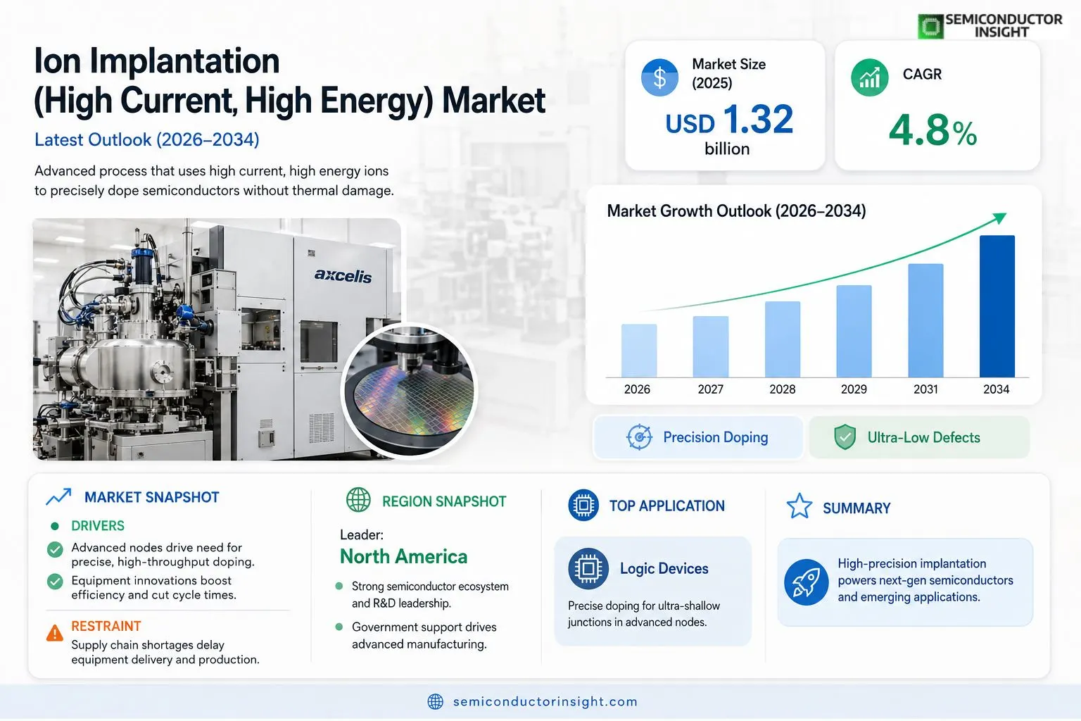
Global ion implantation (high current, high energy) market size was valued at USD 1.32 billion in 2025. The market is projected to grow from USD 1.32 billion in 2025 to USD 2.05 billion by 2034, exhibiting a CAGR of 4.8% during the forecast period.
Ion implantation (high current, high energy) is a semiconductor fabrication technique that accelerates dopant ions to energies typically above 200 keV while delivering currents exceeding 10 mA·cm⁻², enabling precise modification of substrate electrical properties without thermal damage because it provides superior depth control and uniformity compared with diffusion processes; it underpins advanced device architectures such as FinFETs and power MOSFETs furthermore supporting emerging applications in photonics and quantum computing where ultra‑shallow junctions and low defect densities are critical.
MARKET DRIVERS
Increasing Demand in Semiconductor Fabrication
The proliferation of advanced logic nodes and 3‑D IC architectures is driving a steady increase in the adoption of Ion Implantation (High Current, High Energy) technology. Manufacturers require precise dopant profiles at depth, and high‑current systems provide the throughput needed for volume production while maintaining tight defect control.
Advancements in Equipment Efficiency
Recent innovations such as plasma‑based ion sources and real‑time beam monitoring have enhanced process stability and reduced cycle times. These technological gains lower the total cost of ownership, making high‑energy implantation more attractive for both mature and emerging market segments.
➤ Industry analysts project a compound annual growth rate of approximately 8% for high‑current implantation equipment through 2030, reflecting robust capacity expansion.
Overall, the convergence of demand for finer geometries, higher throughput, and equipment efficiencies positions Ion Implantation (High Current, High Energy) Market for sustained expansion.
MARKET CHALLENGES
Technical Complexity and Capital Intensity
Deploying high‑current, high‑energy ion beams demands sophisticated vacuum infrastructure and precise thermal management. The significant upfront investment and specialized expertise required can deter smaller fabs from adopting the technology.
Other Challenges
Regulatory and Environmental Constraints
Stringent emissions regulations around ionizing radiation and hazardous gases impose additional compliance costs, limiting rapid adoption in regions with tight environmental standards.
MARKET RESTRAINTS
Supply Chain Vulnerabilities
Global shortages of high‑purity gases and critical components such as magnetron power supplies create bottlenecks that can delay equipment rollout and affect production schedules, especially during periods of heightened demand.
MARKET OPPORTUNITIES
Expansion into Emerging Applications
Beyond traditional microelectronics, sectors like power electronics, photonics, and quantum device manufacturing are beginning to leverage high‑current, high‑energy ion implantation for material conditioning and defect engineering. This cross‑industry diffusion opens new revenue streams and encourages diversification of the technology portfolio.
Ion Implantation (High Current, High Energy) Market Trends
Increasing Adoption in Advanced Node Devices
The semiconductor industry is accelerating the shift toward sub‑10 nm technology nodes, where precise dopant placement and minimal lattice damage are essential. Ion Implantation (High Current, High Energy) offers superior depth control and uniformity, enabling the formation of ultra‑shallow junctions required for FinFET and power MOSFET architectures. As device geometries shrink, manufacturers are prioritizing processes that reduce thermal budgets while maintaining electrical performance. This drive is prompting fab facilities to upgrade their implantation equipment, integrate real‑time dose monitoring, and adopt advanced beam‑target designs. The result is a measurable increase in process yield and a reduction in defect density, supporting the broader transition to next‑generation logic and power devices.
Other Trends
Integration with Photonic and Quantum Platforms
Beyond traditional CMOS, emerging photonic circuits and quantum computing chips rely on precise material modification to achieve low‑loss waveguides and coherent qubit control. High current, high energy implantation provides the ability to introduce dopants at depths that align with optical mode fields, improving confinement and reducing scattering losses. In quantum devices, the technique minimizes defect generation, which is critical for maintaining qubit coherence times. Early adopters in research labs are reporting increased device reliability and performance consistency, encouraging commercial players to consider dedicated implantation modules tailored for these specialized applications.
Supply Chain Optimization and Equipment Innovation
Manufacturers are responding to the growing demand by streamlining the supply chain for implantation tools and consumables. Collaborative programs between equipment vendors and semiconductor fabs are reducing lead times for critical components such as ion sources and beamline optics. Meanwhile, advancements in power supply modulation and plasma‑based ion generation are delivering higher throughput without compromising beam quality. These innovations are enabling cost‑effective scaling of high‑current, high‑energy processes across a broader range of production volumes, reinforcing the market’s trajectory toward more versatile and resilient fabrication ecosystems.
COMPETITIVE LANDSCAPEKey Industry Players
Ion Implantation (High Current, High Energy) Market Competitive Overview
The ion implantation segment is dominated by a few vertically integrated equipment manufacturers that combine deep research capabilities with global service networks. Applied Materials leads the market with a broad portfolio of high‑current, high‑energy implant systems tailored for FinFET and power device production, leveraging its extensive semiconductor fab relationships to secure long‑term supply contracts. Axcelis Technologies follows closely, differentiating itself through specialized ion source technology that delivers superior beam uniformity and process repeatability, making it a preferred supplier for advanced logic and RF applications. Both firms benefit from scale economies, robust R&D pipelines, and strategic acquisitions that reinforce their positions as the primary sources for high‑volume implant capacity in North America, Europe, and East Asia.
Beyond the dominant players, a diverse set of niche manufacturers contributes critical innovation and regional competitiveness. Nissin Ion Equipment of Japan focuses on compact, high‑precision implantors that serve emerging photonics and quantum‑computing fab lines. Varian Semiconductor, now part of Agilent Technologies, offers ultra‑high‑energy platforms that enable ultra‑deep junction formation for power MOSFETs, securing a strong foothold in the automotive semiconductor space. Tokyo Electron supplies integrated ion implantation modules within its broader equipment suites, attracting customers seeking single‑vendor fab automation. Hitachi High‑Tech, IONEX, Ion Beam Services, NEC Corporation, and others provide tailored solutions for specialty markets such as MEMS, LED, and specialty ICs, ensuring that the ecosystem remains resilient and responsive to evolving technology roadmaps.
List of Key Ion Implantation (High Current, High Energy) Companies Profiled
- Applied Materials Inc.
- Axcelis Technologies, Inc.
- Nissin Ion Equipment Co., Ltd.
- Varian Semiconductor (Agilent Technologies)
- Tokyo Electron Limited
- Hitachi High‑Tech Corporation
- IONEX
- Ion Beam Services (IBS)
- NEC Corporation
- Lam Research Corporation
- Beijing YIJIANG Technology Co., Ltd.
- UltraTech Microsystems
- Quantum Materials Ltd.
Segment Analysis:
| Segment Category | Sub-Segments | Key Insights |
| By Type |
|
Combined High‑Current & High‑Energy is the leading segment because it delivers the depth precision and uniformity required for next‑generation device architectures.
|
| By Application |
|
Logic Devices dominate because precise doping is critical for nanometer‑scale transistors.
|
| By End User |
|
Semiconductor Foundries are the primary adopters, leveraging the technology to meet the relentless demand for scaling.
|
| By Technology |
|
Single‑Wafer Implanters lead the segment due to their flexibility and precision.
|
| By Device Class |
|
Memory Devices emerge as the dominant class, benefitting from high‑current, high‑energy implantation for densely packed 3D architectures.
|
Regional Analysis: North America
United States
The growth of advanced packaging technologies, such as 2.5D and 3D integration, is a key driver for high current, high energy ion implantation. Precise dopant profiles are essential for ensuring reliable interconnects and enhancing device performance in these complex packages.
The increasing adoption of high-power semiconductors in electric vehicles, renewable energy systems, and industrial applications is creating significant demand for ion implantation to improve the efficiency and reliability of power devices.
A key trend in the US market is the ongoing optimization of ion implantation processes to reduce defects, improve throughput, and enhance energy efficiency. This involves advancements in ion source technology, beam diagnostics, and process control systems.
Government initiatives aimed at bolstering domestic semiconductor manufacturing capabilities are providing further impetus to the growth of the ion implantation market in the United States.
Europe
Europe presents a significant and steadily growing market for Ion Implantation (High Current, High Energy). Driven by strong industrial foundations, particularly in automotive and aerospace sectors, the demand for advanced semiconductor components is consistently increasing. The European Union’s commitment to technological leadership and its substantial investments in research and development are fostering innovation in ion implantation processes. Business strategies in Europe frequently involve partnerships between industry, academia, and research institutions to accelerate technology development and address evolving market needs. The market is characterized by a focus on energy efficiency and sustainable manufacturing practices, influencing the adoption of advanced ion implantation techniques. The semiconductor industry in Europe is actively seeking to enhance the performance and reliability of electronic devices through precise ion implantation.
Asia-Pacific
Asia-Pacific is the fastest-growing region for Ion Implantation (High Current, High Energy) Market. Led by countries like China, Japan, and South Korea, this region benefits from a rapidly expanding semiconductor industry, strong government support for technological advancements, and substantial investments in manufacturing infrastructure. The demand for high-performance microchips in consumer electronics, automotive applications, and industrial automation is fueling the need for high current and high energy ion implantation. Strategic business strategies in Asia-Pacific often involve localized manufacturing, close collaboration with local partners, and a focus on cost-effectiveness. The region is witnessing an increasing emphasis on developing indigenous ion implantation technologies and reducing reliance on foreign suppliers. The rapid expansion of the electronics sector in Asia-Pacific presents significant opportunities for growth in the ion implantation market.
South America
South America represents a developing market for Ion Implantation (High Current, High Energy), primarily driven by the growth of the electronics and telecommunications industries. While currently smaller than other regions, the market is expected to witness steady expansion in the coming years. The increasing adoption of smartphones, IoT devices, and industrial automation systems is contributing to the rising demand for advanced semiconductor components and, consequently, for precise ion implantation. Business strategies in South America often focus on providing cost-effective solutions and fostering partnerships with local electronics manufacturers.
Middle East & Africa
The Middle East & Africa region presents a nascent but promising market for Ion Implantation (High Current, High Energy). The growth of the telecommunications sector, increasing investments in infrastructure development, and emerging automotive industries are creating demand for sophisticated electronic components. While the market is relatively small, it has significant potential for future growth as these industries continue to expand. Business strategies in this region often involve focusing on specific niche applications and providing customized solutions to meet local market needs. The increasing emphasis on digitalization and smart city initiatives is expected to further drive the adoption of ion implantation technologies.
Report Scope
This market research report provides a comprehensive analysis of the Ion Implantation (High Current, High Energy) Market , covering the forecast period 2026–2034. It offers detailed insights into market dynamics, technological advancements, competitive landscape, and key trends shaping the industry.
Key focus areas of the report include:
- Market Overview: The report begins with an overview outlining its current market scenario, key growth indicators, and industry transformation drivers. It discusses macroeconomic factors, demand–supply balance, regulatory landscape, and the strategic role of semiconductors in powering advancements across industries such as automotive, telecommunications, consumer electronics, and industrial automation.
- Market Size & Forecast: Historical data and future projections for revenue, unit shipments, and market value across major regions and segments.
- Segmentation Analysis: Detailed breakdown by product type, technology, application, and end-user industry to identify high-growth segments and investment opportunities.
- Regional Insights: Insights into market performance across North America, Europe, Asia-Pacific, Latin America, and the Middle East & Africa, including country-level analysis where relevant.
- Competitive Landscape: Profiles of leading market participants, including their product offerings, R&D focus, manufacturing capacity, pricing strategies, and recent developments such as mergers, acquisitions, and partnerships.
- Technology Trends & Innovation: Assessment of emerging technologies, integration of AI/IoT, semiconductor design trends, fabrication techniques, and evolving industry standards.
- Market Drivers & Restraints: Evaluation of factors driving market growth along with challenges, supply chain constraints, regulatory issues, and market-entry barriers.
- Stakeholder Insights: Insights for component suppliers, OEMs, system integrators, investors, and policymakers regarding the evolving ecosystem and strategic opportunities.
Primary and secondary research methods are employed, including interviews with industry experts, data from verified sources, and real-time market intelligence to ensure the accuracy and reliability of the insights presented.
FREQUENTLY ASKED QUESTIONS:
What is the current market size of Ion Implantation (High Current, High Energy) Market?
-> Ion Implantation (High Current, High Energy) Market was valued at USD 1.32 billion in 2025 and is expected to reach USD 2.05 billion by 2034.
Which key companies operate in Ion Implantation (High Current, High Energy) Market?
-> Key players include Axalta Coating Systems, AkzoNobel, BASF SE, PPG, Sherwin-Williams, and 3M, among others.
What are the key growth drivers?
-> Key growth drivers include railway infrastructure investments, urbanization, and demand for durable coatings.
Which region dominates the market?
-> Asia-Pacific is the fastest-growing region, while Europe remains a dominant market.
What are the emerging trends?
-> Emerging trends include bio-based coatings, smart coatings, and sustainable rail solutions.

Get Sample Report PDF for Exclusive Insights
Report Sample Includes
- Table of Contents
- List of Tables & Figures
- Charts, Research Methodology, and more...
 Download Sample Report PDF


