
High Technology PCB Market Insights
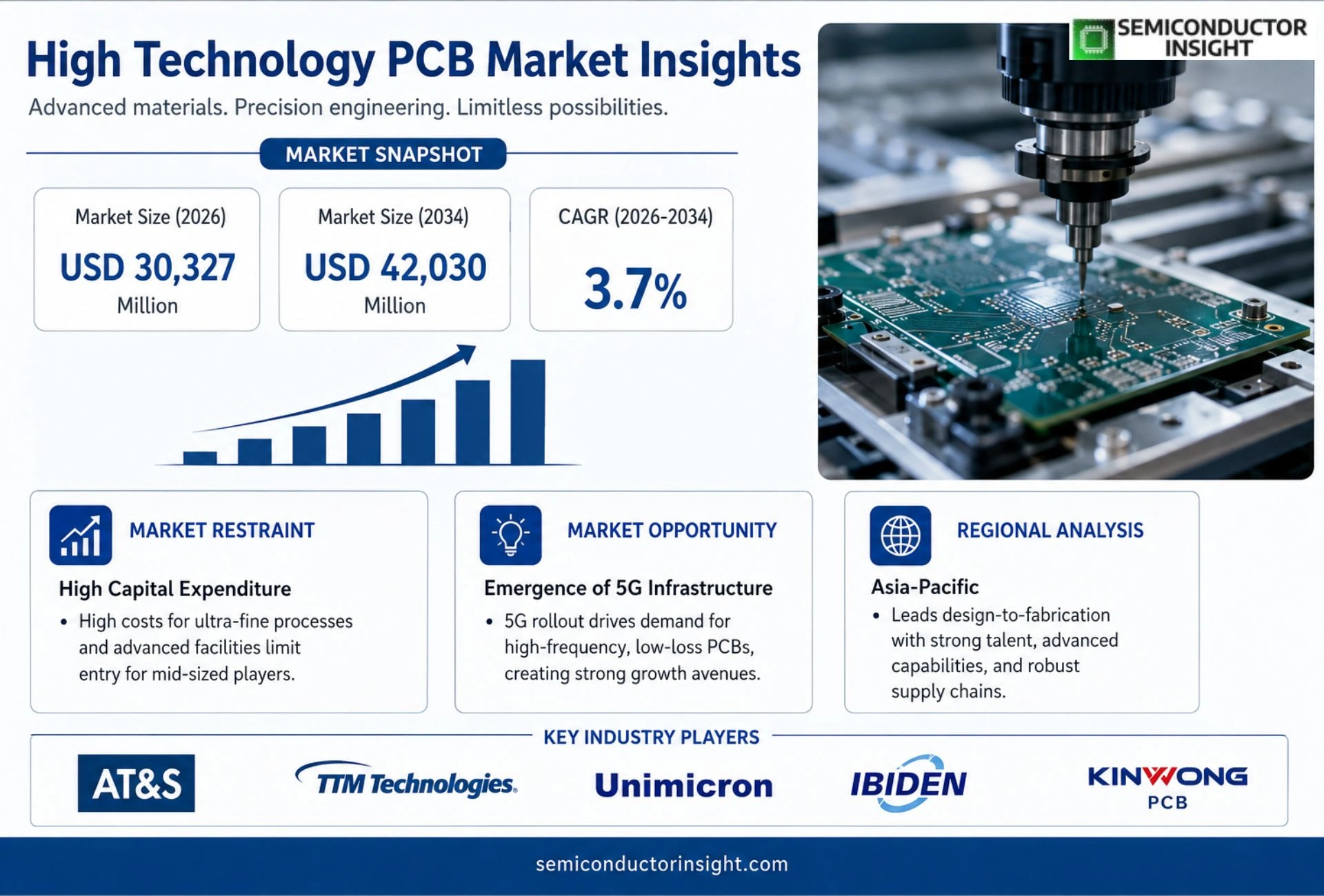
High Technology PCB market is projected to grow from USD 30,327 million in 2026 to USD 42,030 million by 2034, exhibiting a CAGR of approximately 3.7% during the forecast period.
High Technology PCBs represent an advanced class of printed circuit boards that go beyond conventional single‑layer designs. They include multi‑layer rigid boards, high‑density interconnect (HDI), rigid‑flex hybrids, heavy‑copper constructions and high‑frequency variants engineered for demanding applications such as AI‑enabled devices, fifth‑generation wireless infrastructure and electric‑vehicle power systems.
MARKET DRIVERS
Miniaturization Demands in Advanced Electronics
High Technology PCB Market is responding to relentless pressure for smaller, lighter devices. Engineers are packing more functionality into tighter footprints, which forces substrate manufacturers to adopt finer line‑width technologies and innovative stack‑up architectures. This shift not only extends product cycles but also creates recurring revenue streams for suppliers that can deliver ultra‑thin, high‑density boards.
Stringent Performance Standards for Aerospace and Defense
Mission‑critical platforms require printed circuit boards that can endure extreme temperature swings, vibration, and electromagnetic interference. The need for boards with superior thermal conductivity and reliability propels investment in advanced materials such as ceramic‑filled laminates and copper‑foil innovations. Companies that master these specifications gain preferential access to long‑term contracts and higher margins.
➤ “Design flexibility has become a decisive factor when OEMs select a PCB partner.”
Beyond product performance, the competitive edge now hinges on speed to market. Rapid prototyping capabilities combined with agile supply networks enable manufacturers to shorten design‑to‑production timelines, a factor that directly influences OEMs’ ability to capture market share in fast‑moving sectors.
MARKET CHALLENGES
Supply Chain Volatility
Fluctuations in raw‑material availability, especially copper and specialty resins, have created intermittent bottlenecks. When key inputs become scarce, lead times extend, and costs rise, eroding the price advantage of low‑margin producers. Firms that lack diversified sourcing strategies are forced to absorb cost shocks or face order cancellations.
Other Challenges
Regulatory Compliance
Stringent environmental regulations across Europe and Asia impose tighter limits on halogenated compounds and hazardous waste. Compliance requires costly process upgrades and continuous monitoring, which can deter smaller players from scaling up operations.
MARKET RESTRAINTS
High Capital Expenditure for Ultra‑Fine Processes
Transitioning to sub‑micron line widths and multi‑layer stack‑ups demands sophisticated equipment, clean‑room facilities, and skilled labor. The upfront outlay often exceeds the financial capacity of mid‑size manufacturers, limiting market entry and consolidating power among a handful of well‑capitalized players. This concentration curtails competitive pricing and slows diffusion of innovative designs.
MARKET OPPORTUNITIES
Emergence of 5G Infrastructure
The rollout of 5G networks calls for high‑frequency, low‑loss PCBs that can support millimeter‑wave signals. This technical requirement aligns closely with the capabilities of High Technology PCB Market, opening avenues for manufacturers that can deliver low‑dielectric‑constant materials and precision‑etched layouts. Early movers stand to capture sizeable portions of the telecom equipment supply chain as network operators expand coverage.
High Technology PCB Market Trends
Shift Toward Ultra‑High Density Interconnects
High Technology PCB Market is witnessing a decisive move toward ultra‑high density interconnect (UHDI) architectures. As AI accelerators and 5G front‑end modules demand ever tighter signal routing, manufacturers are expanding from traditional double‑layer designs to six‑ and eight‑layer HDI stacks that integrate micro‑vias and sequential lamination. This engineering shift reduces board footprint while preserving high‑speed performance, allowing device makers to meet aggressive form‑factor targets without sacrificing bandwidth. However, the heightened layer count drives up material usage and mandates tighter process control, which in turn raises production costs. Companies that invest early in advanced lithography and automated inspection are gaining a competitive edge, because they can offer reliable UHDI solutions at margins that still satisfy end‑customer price expectations. The trend is reinforced by the rollout of 400‑Gbps Ethernet standards, which forces designers to tighten trace geometry and adopt low‑loss dielectric materials. Firms that can qualify these materials quickly gain head‑to‑head advantage in high‑speed networking segments.
Other Trends
Supply‑Chain Realignment in Asia‑Pacific
Supply‑chain realignment across the Asia‑Pacific region is reshaping High Technology PCB Market’s competitive terrain. Mainland China now hosts the majority of high‑volume production lines, leveraging economies of scale and a mature component ecosystem to deliver lower unit costs. This concentration, however, introduces exposure to trade policy shifts and raw‑material price volatility that can ripple through downstream manufacturers. Several Taiwanese and South Korean firms are diversifying by establishing joint ventures in Southeast Asia, aiming to balance cost advantages with geographic risk mitigation. For original equipment manufacturers, the emerging multi‑hub network offers opportunities to negotiate better terms, but it also obliges them to manage more complex logistics and quality oversight across disparate facilities. Additionally, local governments in Vietnam and Malaysia are offering subsidies for high‑tech PCB production, encouraging smaller players to upscale their capabilities. This policy support gradually diversifies the supplier base, providing buyers with alternative sources without compromising quality.
Emergence of Flexible and Heavy‑Copper Solutions
The rise of flexible and heavy‑copper board formats is another pivotal development within High Technology PCB Market. Automotive electrification and the expanding electric‑vehicle charging infrastructure demand substrates that can tolerate high current densities while sustaining repeated bending cycles. Rigid‑flex constructions address these requirements by merging the mechanical resilience of conventional boards with the pliability needed for tight packaging, whereas heavy‑copper stacks provide the thermal dissipation essential for power‑train modules. Adoption of these solutions compels manufacturers to upgrade to thicker copper lamination presses and to refine adhesive chemistries, investments that increase capital intensity but also open new revenue streams. End‑users benefit from reduced weight and improved reliability, translating into stronger value propositions for vehicle makers and, consequently, greater demand for differentiated PCB capabilities. Moreover, the push toward autonomous driving platforms amplifies the need for reliable signal integrity across densely populated sensor arrays, further driving demand for hybrid board solutions that combine flexibility with robust power delivery.
COMPETITIVE LANDSCAPE
Key Industry Players
High Technology PCB Market – Competitive Overview
Zhen Ding Technology continues to dominate the high‑technology PCB segment thanks to its aggressive capacity expansion in mainland China and a product portfolio that spans HDI, rigid‑flex and heavy‑copper solutions. Its scale allows it to negotiate favorable raw‑material terms, while a strong focus on precision engineering has secured long‑term contracts with leading smartphone and automotive OEMs. TTM Technologies leverages a global footprint that couples U.S. design expertise with Asian manufacturing efficiency, positioning it as a preferred supplier for high‑frequency and aerospace applications. Unimicron, another heavyweight, has differentiated itself through a robust R&D pipeline targeting 5G antenna modules, which translates into higher margins and a resilient order book despite cyclical pressure on commodity PCBs.
Beyond the tier‑one giants, a cohort of specialized firms is reshaping niche corridors of the market. Mektec’s emphasis on high‑density interconnect (HDI) for AI accelerators has earned it a reputation for ultra‑thin, high‑performance boards, while DSBJ focuses on heavy‑copper substrates tailored for power‑train modules in electric vehicles. Companies such as Kingboard, Ibiden and AT&S have built strategic alliances with semiconductor manufacturers, securing a pipeline of demand from next‑generation graphics and compute products. Smaller players like Meiko, Daeduck Group and Kinwong concentrate on regional supply chains in Korea and Taiwan, offering rapid turn‑around services that appeal to start‑ups seeking low‑volume, high‑mix production. Collectively, this diverse ecosystem creates a competitive matrix where scale, technological depth and geographic agility dictate market positioning.
List of Key High Technology PCB Companies Profiled
- Zhen Ding Technology
- TTM Technologies
- Unimicron
- Mektec
- DSBJ
- Compeq Manufacturing
- Tripod Technology
- Shennan Circuits Company
- HannStar Board (GBM)
- SEMCO
- Kingboard
- Ibiden
- WUS
- Young Poong
- AT&S
- Meiko
- Daeduck Group
- Nanya PCB
- Fujikura
- Kinwong
- CMK
- Sunshine Global Circuits
Segment Analysis:
| Segment Category | Sub-Segments | Key Insights |
| By Type |
|
HDI is emerging as the leading segment because:
|
| By Application |
|
Communication drives the market due to:
|
| By End User |
|
OEMs dominate because:
|
| By Technology Innovation |
|
Advanced Materials are pivotal because:
|
| By Market Driver |
|
5G Deployment fuels growth because:
|
Regional Analysis: High Technology PCB Market
Asia‑Pacific
An extensive network of PCB fabricators across the Yangtze Delta delivers economies of scale while investing in high‑precision etching and laser drilling. These capabilities allow rapid transition from prototype to full‑volume production, a decisive factor for customers pursuing aggressive product launch timelines.
Japan’s focus on specialty laminates and low‑dielectric‑constant substrates fuels differentiation for high‑speed communications boards. Collaboration between material suppliers and OEMs yields bespoke solutions that address thermal management challenges in dense circuitry.
Strong R&D incentives encourage Korean firms to explore 3D‑stacked architectures and embedded component technologies. The resulting design expertise attracts multinational brands seeking cutting‑edge form factors for wearable and IoT devices.
Vietnam’s growing cadre of skilled technicians and lower operational costs position it as an emerging alternative for volume assembly of high‑performance boards, especially as larger manufacturers diversify their geographic footprint.
North America
In North America, High Technology PCB Market reflects a demand pattern driven by defense procurement and a mature automotive electronics sector. End‑users prize reliability and traceability, prompting suppliers to adopt stringent quality certifications and advanced process monitoring. The region’s emphasis on sustainability influences material selection, with several firms exploring bio‑based laminates. While labor costs remain higher than in Asia‑Pacific, the proximity to key customers and the ability to provide rapid prototyping services sustain a competitive edge for domestic manufacturers.
Europe
European stakeholders balance regulatory compliance with a push toward miniaturization in medical and aerospace applications. The continent’s strong patent portfolio in high‑frequency interconnects fosters a market for specialized, low‑loss boards. Collaborative R&D initiatives, often funded through Horizon programmes, accelerate adoption of next‑generation dielectric technologies. Although cost pressures compel some firms to outsource production, many retain in‑house capabilities to safeguard intellectual property and meet strict certification timelines demanded by aerospace clients.
South America
South America’s involvement in High Technology PCB Market is anchored by a gradual shift from consumer‑grade to performance‑oriented products. Automotive manufacturers seeking electric‑vehicle components are encouraging local PCB assemblers to upgrade process capabilities. Government incentives aimed at technology parks are attracting foreign investors, which introduces advanced equipment and expertise. The market remains fragmented, but a rising demand for reliable high‑density interconnects hints at a maturing ecosystem.
Middle East & Africa
The Middle East & Africa region experiences modest yet steady interest in high‑performance printed circuit boards, primarily driven by telecom expansion and renewable‑energy installations. Strategic location advantages enable regional distributors to serve both African markets and Asian exporters. Partnerships between local firms and established Asian manufacturers are fostering knowledge transfer, gradually enhancing design competence. Although the market’s scale is limited, emerging smart‑city projects are expected to create niche opportunities for specialized PCB solutions.
Report Scope
This market research report provides a comprehensive analysis of the High Technology PCB Market , covering the forecast period 2026–2034. It offers detailed insights into market dynamics, technological advancements, competitive landscape, and key trends shaping the industry.
Key focus areas of the report include:
- Market Overview: The report begins with an overview outlining its current market scenario, key growth indicators, and industry transformation drivers. It discusses macroeconomic factors, demand–supply balance, regulatory landscape, and the strategic role of semiconductors in powering advancements across industries such as automotive, telecommunications, consumer electronics, and industrial automation.
- Market Size & Forecast: Historical data and future projections for revenue, unit shipments, and market value across major regions and segments.
- Segmentation Analysis: Detailed breakdown by product type, technology, application, and end-user industry to identify high-growth segments and investment opportunities.
- Regional Insights: Insights into market performance across North America, Europe, Asia-Pacific, Latin America, and the Middle East & Africa, including country-level analysis where relevant.
- Competitive Landscape: Profiles of leading market participants, including their product offerings, R&D focus, manufacturing capacity, pricing strategies, and recent developments such as mergers, acquisitions, and partnerships.
- Technology Trends & Innovation: Assessment of emerging technologies, integration of AI/IoT, semiconductor design trends, fabrication techniques, and evolving industry standards.
- Market Drivers & Restraints: Evaluation of factors driving market growth along with challenges, supply chain constraints, regulatory issues, and market-entry barriers.
- Stakeholder Insights: Insights for component suppliers, OEMs, system integrators, investors, and policymakers regarding the evolving ecosystem and strategic opportunities.
Primary and secondary research methods are employed, including interviews with industry experts, data from verified sources, and real-time market intelligence to ensure the accuracy and reliability of the insights presented.
FREQUENTLY ASKED QUESTIONS:
What is the current market size of High Technology PCB Market?
-> High Technology PCB Market was valued at USD 29,260 million in 2024 and is expected to reach USD 37,720 million by 2031, growing at a CAGR of 3.8% during the forecast period.
Which key companies operate in High Technology PCB Market?
-> Key players include Zhen Ding Tech, TTM Technologies, Unimicron, Mektec, DSBJ, Compeq Manufacturing, Tripod, Shennan Circuits Company, HannStar Board (GBM), SEMCO, Kingboard, Ibiden, Wus, Young Poong, AT&S, Meiko, Daeduck Group, Nanya PCB, Fujikura, Kinwong, CMK, Sunshine Global Circuits.
What are the key growth drivers?
-> Key growth drivers include advancements in AI, 5G deployment, new energy vehicles, and increasing demand for high‑performance PCBs such as HDI, Rigid‑Flex and Heavy Copper types.
Which region dominates the market?
-> Asia dominates High Technology PCB Market, with Chinese mainland manufacturers holding the largest share, followed by Taiwan, Japan and South Korea.
What are the emerging trends?
-> Emerging trends include the shift from single‑layer to multi‑layer and HDI designs, increased adoption of Rigid‑Flex and Heavy Copper PCBs, and the integration of high‑frequency and high‑speed technologies to support next‑generation communications and automotive electrification.

Get Sample Report PDF for Exclusive Insights
Report Sample Includes
- Table of Contents
- List of Tables & Figures
- Charts, Research Methodology, and more...
 Download Sample Report PDF


