HBM2E DRAM Market Insights
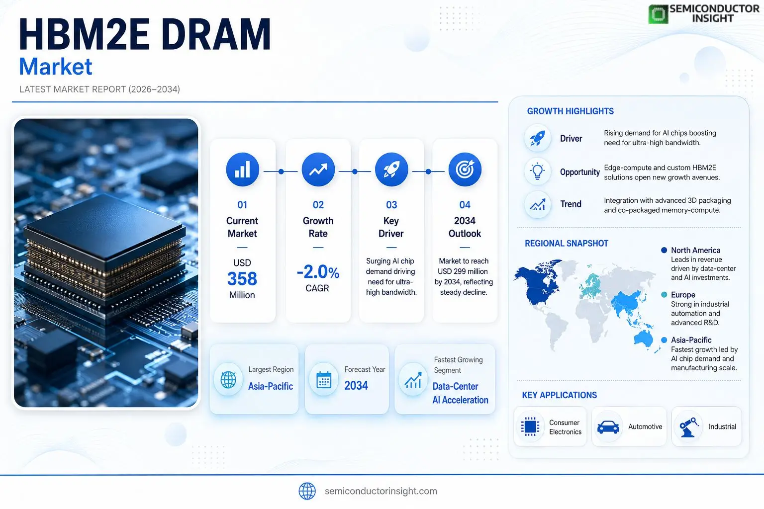
HBM2E DRAM market size was valued at USD 358 million in 2025 and is expected to fall to approximately USD 299 million by 2034, reflecting a CAGR of –2.0 % over the period.
HBM2E DRAM is a high‑bandwidth stacked dynamic random‑access memory designed for high‑performance computing, AI training, machine learning, predictive modeling, servers, networking and advanced graphics systems. Its core purpose is to provide GPUs, ASICs and other accelerators with bandwidth density far above that of traditional discrete graphics memory while remaining within limited package area and power budgets.Official specifications indicate typical devices employ four or eight DRAM layers beneath a logic base in a three‑dimensional integrated stack; TSVs, silicon interposers or very wide I/O links bring the memory into close proximity with the host chip. This architecture delivers aggregate bandwidth of roughly 410–460 GB/s at per‑pin data rates of 3.2–3.6 Gbps, improves capacity utilization and reduces board‑level routing complexity.The primary customers are GPU designers, AI accelerator developers, supercomputing system integrators and high‑end server manufacturers rather than consumer electronics brands. Delivery usually follows an advanced packaging or system‑in‑package flow together with the host ASIC, creating a high‑value B₂B supply chain where joint validation between memory supplier and platform designer is essential.
MARKET DRIVERS
Rising AI Chip Demand
The surge in artificial‑intelligence accelerators has forced silicon designers to prioritize memory that can feed massive parallel engines without throttling. HBM2E DRAM Market benefits because its stacked architecture delivers up to three times the bandwidth of conventional DDR solutions, letting AI inference stay within power envelopes while scaling model size.
Bandwidth‑Intensive Data‑Center Deployments
Hyperscale operators are migrating to servers that host multi‑chip‑module GPUs for training workloads. The tighter integration between processor and stacked DRAM reduces latency spikes, a factor that directly translates into higher throughput per rack. Vendors that can ship HBM2E modules at the required density gain a measurable edge in capacity planning.
➤ “Every extra 10 GB/s of sustained bandwidth can shave weeks off model training cycles, thereby accelerating time‑to‑revenue for AI‑driven services.”
Beyond pure performance, the low‑power profile of HBM2E satisfies data‑center sustainability targets. Operators increasingly weigh energy‑efficiency alongside raw speed, and the stacked design helps lower the total cost of ownership for high‑performance compute clusters.
MARKET CHALLENGES
Cost Sensitivity in GPU Platforms
Even though HBM2E offers clear technical merits, its per‑gigabyte price remains substantially higher than legacy alternatives. System integrators must justify the premium through demonstrable productivity gains, a hurdle for midsize players that cannot absorb the expense without impacting margins.
Other Challenges
Manufacturing Yield Constraints
The intricate TSV (through‑silicon‑via) process that underpins stacked DRAM drives yield variability. Any dip in yield translates into delayed shipments and tighter supply, pressuring OEMs to maintain buffer inventories.
MARKET RESTRAINTS
Thermal Management Limits
Stacked memory piles generate concentrated heat zones that challenge conventional cooling solutions. Designers must allocate additional silicon area for heat spreaders, which erodes the density advantage that HBM2E promises.
Supply‑Chain Vulnerabilities
Recent geopolitical tensions have exposed the fragility of the specialized fabs that produce high‑bandwidth stacks. Any disruption forces downstream OEMs to seek alternate sources, often at higher cost and longer lead times.
Competing Memory Technologies
Emerging alternatives such as compute‑in‑memory fabrics and next‑generation DDR5 with on‑die buffers are narrowing the performance gap, prompting some designers to defer HBM2E adoption until a clear advantage is evident.
MARKET OPPORTUNITIES
Emerging Edge‑Compute Architectures
Edge AI processors require high bandwidth in a compact footprint to enable real‑time analytics without offloading to the cloud. HBM2E’s stacked form factor aligns with the size constraints of edge modules, opening pockets of growth in automotive, surveillance, and industrial IoT segments.
Strategic Partnerships with Foundries
Collaborations between memory vendors and advanced‑node foundries are accelerating the rollout of 3‑nm‑compatible HBM2E stacks. These alliances reduce time‑to‑market for next‑generation GPUs, offering a pathway for early adopters to differentiate on performance.
Custom‑Design Services
OEMs are increasingly requesting tailor‑made memory configurationsvarying stack heights, pitch, and power envelopes. Providers that can deliver bespoke HBM2E solutions stand to capture premium pricing while strengthening long‑term client relationships.
HBM2E DRAM Market Trends
Consolidated Supplier Landscape and Platform Lock‑In
The HBM2E DRAM ecosystem is dominated by three manufacturersSamsung, SK Hynix, and Micronwhose ability to deliver 16 GB stacks with 3.2‑3.6 Gbps I/O speeds hinges on advanced 3‑D integration and silicon‑interposer expertise. Because the memory is sold as a kilogram‑scale device (KGSD) that must be co‑packaged with a host ASIC, entry requires not only wafer‑fab capacity but also deep joint‑validation programs with GPU and AI‑accelerator designers. This dual‑gate creates a de‑facto platform lock‑in: once a supplier secures a flagship GPU design, subsequent generations of that platform tend to stay with the same memory partner, resulting in stable, long‑term revenue streams but limited competitive pressure on pricing. Customers, therefore, prioritize supply‑chain reliability and engineering support over marginal cost differences, shaping procurement strategies that favor established relationships.
Other Trends
Energy Efficiency as a Competitive Lever
HBM2E’s stacked architecture reduces per‑pin data rates while delivering 410‑460 GB/s aggregate bandwidth, a combination that translates into markedly lower power consumption compared with GDDR alternatives. For large‑model AI training and high‑resolution graphics rendering, the thermal headroom gained per watt directly influences datacenter operating costs and chassis design. Vendors that can certify tighter thermal envelopes or demonstrate a measurable reduction in system‑level power draw gain a persuasive value proposition, prompting OEMs to embed those memory parts early in product road‑maps. The ripple effect reaches upstream fabs, which invest in yield‑improving process steps to sustain the efficiency premium, and downstream system integrators, who can shorten cooling subsystem budgets and extend rack density.
Regional Policy Support Influencing Demand
Government initiatives in the United States, the European Union, and China are reshaping the demand profile for high‑bandwidth memory. The U.S. CHIPS Act funds advanced‑packaging infrastructure that directly benefits KGSD production, while the European Chips Act emphasizes supply‑chain resilience, encouraging local fab expansions that may host HBM2E lines. China’s national compute‑infrastructure plan subsidizes AI‑focused supercomputing clusters, indirectly boosting orders for memory that meets tight bandwidth‑per‑area constraints. These policy levers do not create new market categories, but they heighten the attractiveness of projects that already target ultra‑high‑performance workloads, thereby sustaining a baseline of orders for HBM2E devices even as newer generations emerge. Investors and OEMs attentive to these programs can better anticipate where capacity will be allocated and align product development cycles accordingly.
COMPETITIVE LANDSCAPE
Key Industry Players
HBM2E DRAM Competitive Overview
Samsung Electronics dominates the HBM2E segment with its Flashbolt portfolio, leveraging a vertically integrated fabs‑to‑packaging model that shortens time‑to‑market for 16 GB stacks. SK Hynix follows closely, differentiating its offering through aggressive bandwidth targets (up to 3.6 Gbps per pin) and a strong foothold in the Korean ecosystem that aligns silicon‑interposer capacity with major GPU vendors. Micron Technology, the only North‑American supplier, concentrates on a KGSD delivery flow, pairing its HBM2E products with mature OSAT partners to meet the stringent thermal and power envelopes demanded by AI accelerators. The tri‑metal structure creates an oligopolistic market where entry barriers hinge on 3‑D stacking expertise, TSV yield control, and long‑run customer qualification cycles, resulting in platform lock‑in that shapes revenue stability for the incumbents.Beyond the three giants, a constellation of niche and ecosystem players sustains the supply chain. Intel and AMD, while not memory fabs, drive co‑development programs that lock in design‑win cycles for next‑generation GPUs and AI ASICs. NVIDIA’s close collaboration with the fabs accelerates reference designs, reinforcing demand for bespoke HBM2E stacks. OSAT specialists such as ASE Technology Holding and Amkor Technology provide SiP assembly services that are essential for the high‑density interposer approach. Regional players like Powerchip Semiconductor Manufacturing Corp, Nanya Technology, WINBOND Electronics, and China’s ChangXin Memory Technologies contribute capacity in lower‑cost segments or pilot lines, while TSMC’s advanced packaging platform offers an alternative route for fab‑less ASIC developers. These participants collectively expand the ecosystem, but their influence remains secondary to the three primary manufacturers.
List of Key HBM2E DRAM Companies Profiled
- Samsung Electronics
- SK Hynix
- Micron Technology
- Intel Corporation
- Advanced Micro Devices (AMD)
- NVIDIA Corporation
- ASE Technology Holding
- Amkor Technology
- TSMC
- Powerchip Semiconductor Manufacturing Corp
- Nanya Technology Corp
- WINBOND Electronics Corp
- ChangXin Memory Technologies (CXMT)
- Everspin Technologies
Segment Analysis:
| Segment Category | Sub-Segments | Key Insights |
| By Type |
|
Leading Segment – 8‑Layer High‑Bandwidth Stack
|
| By Application |
|
Leading Segment – Data‑Center AI Acceleration Systems
|
| By End User |
|
Leading Segment – GPU Designers
|
| By Stack Architecture |
|
Leading Segment – Silicon Interposer‑Based Interconnect
|
| By Integration Model |
|
Leading Segment – Co‑Packaged Memory‑Compute
|
Regional Analysis: HBM2E DRAM Market
Asia‑Pacific
Foundries in Taiwan and South Korea dominate wafer output, delivering the process fidelity needed for HBM2E’s fine‑pitch interconnects. Their ability to run multiple layers in a single fab minimizes hand‑offs and protects intellectual property, granting regional customers a competitive edge in speed‑to‑revenue.
Regional chipset designers, especially those engaged in AI inference engines, align product roadmaps with HBM2E specifications early in development. This collaborative approach yields memory solutions that are tightly tuned to processor architecture, sharpening performance margins.
A network of diversified silicon wafer suppliers and localized testing facilities cushions the region against external shocks, ensuring that volume ramps for HBM2E can proceed without prolonged bottlenecks.
Government incentives targeting advanced packaging and high‑bandwidth memory encourage R&D investment, while trade agreements streamline component imports, reinforcing the region’s leadership in the HBM2E DRAM Market.
North America
North America’s strength lies in its deep pool of system‑level architects and enterprise‑grade data‑center operators. While most wafer production remains offshore, the continent excels at integrating HBM2E modules into flagship servers and graphics solutions, driving premium pricing. Intellectual‑property licensing and design‑wins from major cloud providers give the market a top‑down pull that forces upstream suppliers to meet stringent latency and thermal budgets. Recent collaborations between U.S. universities and memory manufacturers have also seeded next‑generation packaging concepts, hinting at a future where domestic fab capacity could capture a larger share of the value chain.
Europe
European activity in the HBM2E DRAM Market is anchored by a network of automotive and industrial automation firms that demand deterministic bandwidth and robust reliability. The region’s regulatory environment pushes manufacturers toward eco‑efficient designs, prompting a shift from purely performance‑driven memory to solutions that balance power consumption with endurance. Cross‑border research consortia, particularly in Germany and France, are experimenting with heterogeneous integration techniques that could lower production costs while preserving the high signal integrity required for HBM2E stacks.
South America
In South America, the market remains nascent, yet growth is being fueled by a surge in local semiconductor education programs and government calls for digital sovereignty. Companies are increasingly importing HBM2E‑enabled platforms to support emerging AI startups, creating a modest but steady demand curve. The region’s competitive advantage stems from lower labor costs for assembly and testing, which may attract multinational contract manufacturers seeking cost‑effective final‑stage operations.
Middle East & Africa
The Middle East & Africa region is positioning itself as a strategic logistics hub for high‑bandwidth memory distribution, leveraging its geographic proximity to Asian production sites. Investment in data‑center infrastructure, especially in the Gulf Cooperation Council countries, is prompting early adoption of HBM2E‑based accelerators for cloud services. Meanwhile, African technology parks are exploring edge‑compute deployments that rely on compact, high‑throughput memory, suggesting a long‑term niche for the market as connectivity improves across the continent.
Report Scope
This market research report provides a comprehensive analysis of the HBM2E DRAM Market , covering the forecast period 2026–2034. It offers detailed insights into market dynamics, technological advancements, competitive landscape, and key trends shaping the industry.
Key focus areas of the report include:
- Market Overview: The report begins with an overview outlining its current market scenario, key growth indicators, and industry transformation drivers. It discusses macroeconomic factors, demand–supply balance, regulatory landscape, and the strategic role of semiconductors in powering advancements across industries such as automotive, telecommunications, consumer electronics, and industrial automation.
- Market Size & Forecast: Historical data and future projections for revenue, unit shipments, and market value across major regions and segments.
- Segmentation Analysis: Detailed breakdown by product type, technology, application, and end-user industry to identify high-growth segments and investment opportunities.
- Regional Insights: Insights into market performance across North America, Europe, Asia-Pacific, Latin America, and the Middle East & Africa, including country-level analysis where relevant.
- Competitive Landscape: Profiles of leading market participants, including their product offerings, R&D focus, manufacturing capacity, pricing strategies, and recent developments such as mergers, acquisitions, and partnerships.
- Technology Trends & Innovation: Assessment of emerging technologies, integration of AI/IoT, semiconductor design trends, fabrication techniques, and evolving industry standards.
- Market Drivers & Restraints: Evaluation of factors driving market growth along with challenges, supply chain constraints, regulatory issues, and market-entry barriers.
- Stakeholder Insights: Insights for component suppliers, OEMs, system integrators, investors, and policymakers regarding the evolving ecosystem and strategic opportunities.
Primary and secondary research methods are employed, including interviews with industry experts, data from verified sources, and real-time market intelligence to ensure the accuracy and reliability of the insights presented.
FREQUENTLY ASKED QUESTIONS:
What is the current market size of HBM2E DRAM Market?
-> HBM2E DRAM Market was valued at USD 358 million in 2025 and is expected to reach USD 311 million by 2032, at a CAGR of -2.0% during the forecast period.
Which key companies operate in HBM2E DRAM Market?
-> Key players include SK Hynix, Samsung, and Micron Technology, Inc., among others.
What are the key growth drivers?
-> Key growth drivers include surging demand for high‑performance computing, AI model training, data‑center acceleration, and the need for higher bandwidth‑density memory within limited packaging footprints.
Which region dominates the market?
-> North America (particularly the United States) dominates in terms of revenue, while Asia‑Pacific shows the fastest growth due to strong AI and supercomputing investments.
What are the emerging trends?
-> Emerging trends include integration of HBM2E with advanced 3D‑IC packaging, co‑development between memory suppliers and GPU/AI accelerator designers, and a gradual transition toward HBM3 while maintaining HBM2E in legacy and cost‑sensitive platforms.
Get Sample Report PDF for Exclusive Insights
Report Sample Includes
- Table of Contents
- List of Tables & Figures
- Charts, Research Methodology, and more...
 Download Sample Report PDF