HBM2 DRAM Market Insights
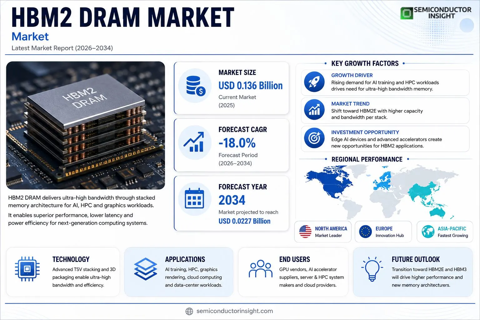
HBM2 DRAM market size was USD 136 million in 2025 and is expected to decline to roughly USD 22.7 million by 2034, indicating an implied compound annual growth rate of about –18 % over the period.
HBM2 memory represents the second generation of high‑bandwidth stacked DRAM engineered for artificial‑intelligence training, high‑performance computing, graphics rendering and other data‑intensive workloads. By employing through‑silicon vias, multiple DRAM layers are vertically integrated with GPUs, CPUs or TPUs within a single package, which shortens signal paths, boosts parallel throughput and improves power‑thermal efficiency. Variants such as HBM2E extend capacity per stack up‑to 16 GB and deliver bandwidth tiers of 307 GB/s, 410 GB/s or 460 GB/s, making them indispensable for large‑model AI accelerators, supercomputing clusters and advanced graphics systems.
MARKET DRIVERS
AI Acceleration Demand
The surge in neural‑network training workloads has forced system architects to seek memory that can deliver terabytes per second of bandwidth. By stacking DRAM dies vertically and employing through‑silicon vias, HBM2 delivers a throughput that outpaces traditional DDR solutions, making it a natural fit for GPUs and accelerators that power large‑scale AI models.
Data‑Center Bandwidth Requirements
Cloud providers are re‑architecting their hyperscale pods to accommodate high‑resolution rendering and real‑time inference. The ability of HBM2 to sustain low latency while moving massive data streams reduces queue buildup in the memory hierarchy, translating into higher utilization of compute engines and lower total cost of ownership for operators.
➤ “HBM2’s capacity scaling unlocks new classes of applications that were previously bandwidth‑constrained,” says a senior engineer at a leading silicon foundry.
The combined effect of AI acceleration demand and data‑center bandwidth pressure is reshaping the HBM2 DRAM Market, prompting vendors to accelerate product roadmaps and invest in advanced packaging.
MARKET CHALLENGES
Manufacturing Complexity
Building HBM2 stacks requires wafer‑level bonding and precise alignment of multiple dies, a process that pushes the limits of current fabrication lines. Yield variability across each die in the stack inflates defect rates, compelling manufacturers to implement costly inspection regimes.
Other Challenges
Cost Competitiveness
The per‑gigabyte price of HBM2 remains markedly higher than that of conventional DDR4, limiting its adoption to premium segments. As AI workloads mature, customers are scrutinizing the cost‑to‑performance ratio, pressuring suppliers to lower prices without sacrificing bandwidth.Beyond cost, the limited pool of design‑ready IP blocks constrains OEMs seeking rapid time‑to‑market, creating a bottleneck that could decelerate broader uptake.
MARKET RESTRAINTS
Supply‑Chain Fragility
HBM2 production depends on a narrow set of advanced fabs located in a few regions. Trade restrictions or unexpected plant shutdowns can ripple through the supply chain, leaving system builders with longer lead times and constrained inventory.High‑density stacking raises thermal density, demanding sophisticated cooling solutions. Companies that cannot integrate effective heat removal may encounter throttling, deterring them from deploying the technology at scale.
MARKET OPPORTUNITIES
Emerging Edge‑AI Devices
Edge devices that run inference locally, such as autonomous drones and AR headsets, require compact memory with bandwidth comparable to data‑center GPUs. HBM2’s stacked architecture offers a pathway to embed high‑speed memory within tight form factors, opening a new revenue stream for memory suppliers.
Coupling HBM2 with next‑generation silicon photonics interconnects promises to further reduce latency across system boundaries. Early collaborations between memory vendors and photonics players signal a niche where the HBM2 DRAM Market can capture premium pricing.
HBM2 DRAM Market Trends
Shift Toward Integrated High‑Bandwidth Stacks
The HBM2 DRAM Market is being reshaped by the migration from discrete memory modules to tightly‑coupled stacked die that sit directly on GPUs, CPUs or AI accelerators. By embedding memory through through‑silicon vias, manufacturers achieve bandwidths that eclipse 400 GB/s per stack while keeping the footprint under a few square centimeters. This architecture directly addresses the data‑movement bottlenecks that limit training of large‑scale AI models and the compute intensity of scientific simulations. As model sizes double roughly every year, system designers are forced to allocate more memory bandwidth per watt, making the high‑density, low‑power profile of HBM2 and its HBM2E evolution a decisive factor in platform selection. The result is a noticeable tilt in system‑level bill‑of‑materials toward custom‑integrated solutions rather than off‑the‑shelf DDR alternatives.
Other Trends
Supply‑Chain Concentration and Regional Reach
Three manufacturers dominate the upstream landscape: Samsung and SK hynix in Korea, and Micron in the United States. Their shared reliance on TSV stacking and advanced packaging creates a high barrier to entry, keeping the supply base narrow yet ly distributed. Each supplier has built support networks that span Asia, Europe, the Middle East and the Americas, allowing them to service data‑center builders in China, AI research labs in Europe, and supercomputing facilities in North America without a significant logistics lag. The concentration of capability translates into pricing power for the incumbents, while downstream demand continues to diffuse across continents as AI workloads proliferate.
Design‑Cycle Complexity and Co‑Development Models
Unlike conventional DRAM, HBM2 devices are delivered as known‑good stacked die that must be co‑packaged with host processors by OSATs or the system integrators themselves. This joint development approach shifts the competitive arena from pure wafer cost to a blend of stacking yield, thermal management, and interposer design. Validation cycles lengthen, and customers often lock in multi‑year supply agreements to guarantee stack‑level performance targets. For vendors, the implication is a move toward longer‑term engineering partnerships and a need to expose deeper technical roadmaps to ensure that future accelerator generations can reliably tap the bandwidth gains offered by HBM2E’s 410 GB/s and 460 GB/s tiers. Companies that can synchronize silicon‑process improvements with packaging innovations are poised to capture the most lucrative contracts in high‑end AI infrastructure.
COMPETITIVE LANDSCAPE
Key Industry Players
HBM2 DRAM Market
Samsung Electronics dominates the HBM2 ecosystem through an integrated approach that couples its advanced TSV stacking capacity with a packaging network. The company’s Aquabolt and Flashbolt families illustrate its depth in both capacity (8‑16 GB per stack) and bandwidth (307‑410 GB/s), which has secured multi‑year design wins with premier GPU vendors and AI‑accelerator makers. Samsung’s ability to control wafer output, stack yield, and thermal optimization translates into a pricing premium that smaller rivals struggle to match. Moreover, its cross‑regional sales infrastructurespanning Korea, China, Europe, and the Americasenables rapid customer support, reinforcing long‑term lock‑in for data‑center and high‑performance‑computing projects.Beyond the three incumbents, a handful of specialist players and advanced‑packaging partners shape the competitive perimeter. SK hynix leverages its HBM2E portfolio, pushing per‑stack speeds to 3.6 Gbps and bandwidths near 460 GB/s, while Micron focuses on tight integration with U.S. AI‑chip designers, supplying known‑good die to OSATs such as Amkor and ASE. Companies like Intel and AMD, though primarily system architects, influence the supply chain by committing large volumes that dictate roadmap timing. Regional OSATsincluding ASE Technology, Amkor Technology, and TSMC’s advanced packaging unitadd a layer of differentiation through yield‑boosting interposer designs. Smaller but technically adept firms such as Nanya Technology and Everspin are beginning to explore niche HBM2 derivatives for embedded and automotive applications, expanding the market beyond the classic GPU‑centric use case.
List of Key HBM2 DRAM Companies Profiled
- Samsung Electronics
- SK Hynix
- Micron Technology
- Intel Corporation
- Advanced Micro Devices
- ASE Technology Holding
- Amkor Technology
- Nanya Technology
- Everspin Technologies
- TSMC Advanced Packaging
- SK Telecom (Strategic Partner)
- Foundries (Design Collaboration)
- PowerVR (NVIDIA Collaboration)
Segment Analysis:
| Segment Category | Sub-Segments | Key Insights |
| By Type |
|
8 GB emerges as the most widely adopted capacity because it balances integration density with manageable thermal design.
|
| By Application |
|
Data Center AI Acceleration Systems dominate the application landscape.
|
| By End User |
|
GPU Vendors hold the leading end‑user position.
|
| By Technology Generation |
|
HBM2E is the leading generation because it delivers higher per‑pin speeds, larger stack capacities, and better thermal efficiency.
|
| By Packaging & Integration |
|
Silicon Interposer Solutions drive the most strategic value.
|
Regional Analysis: HBM2 DRAM Market
Asia‑Pacific
Foundries in Taiwan and South Korea dominate the wafer output for HBM2 stacks, creating a de‑facto hub that streamlines material sourcing and test‑equipment sharing. This concentration lowers unit costs but also makes the region sensitive to capacity shocks, prompting manufacturers to diversify upstream logistics.
Local EDA vendors have matured their 3‑D‑IC design tools, allowing chip architects to iterate memory‑interface layouts with fewer silicon iterations. The synergy between design houses and fab partners shortens time‑to‑market for custom HBM2 solutions.
The surge in AI‑accelerated workloads and high‑resolution gaming drives demand for bandwidth‑dense memory. Chipmakers in the region embed HBM2 stacks directly into GPUs and networking ASICs, unlocking performance margins that are hard to achieve with conventional DRAM.
Government initiatives that subsidise advanced packaging and provide tax relief for R&D have lowered the effective cost of developing new HBM2 process nodes, encouraging both incumbents and startups to push the technology envelope.
North America
In the United States and Canada, the HBM2 DRAM Market is shaped by a strong push from semiconductor design houses that prioritize performance scaling for cloud‑native AI services. While domestic fabs are limited, the region relies heavily on strategic import agreements that guarantee a steady supply of high‑bandwidth memory. Partnerships between chipset vendors and Asian foundries are increasingly formalised through long‑term contracts, ensuring design teams can lock in stack specifications early in product roadmaps. Concurrently, federal investment in next‑generation packaging research is nurturing a nascent domestic ecosystem that could eventually localise a portion of the supply chain, mitigating geopolitical risk.
Europe
European players emphasize sustainability and supply‑chain resilience in their approach to HBM2 memory. Major automotive and industrial automation firms demand memory solutions with stringent reliability standards, prompting manufacturers to adopt stricter testing protocols. The European Union’s semiconductor strategy funds collaborative projects that integrate HBM2 stacks into edge‑compute platforms, positioning the region as a niche supplier for low‑latency, high‑throughput applications. Although the continent lacks large‑scale wafer fabs, its strength lies in design expertise and a regulatory environment that encourages circular‑economy practices, influencing product specifications toward energy‑efficient memory architectures.
South America
South American markets are in an early adoption phase, with demand primarily originating from telecom operators expanding 5G backhaul and from multinational data‑center providers establishing regional hubs. Local distributors act as intermediaries, aggregating orders to meet minimum volume thresholds required by major memory suppliers. While the region does not host manufacturing capacity, emerging partnerships with Asian vendors aim to develop localized testing facilities, which could reduce lead times and enable more responsive servicing of latency‑critical workloads.
Middle East & Africa
The Middle East & Africa region views HBM2 DRAM as an enabler for sovereign cloud initiatives and for high‑performance scientific computing projects tied to oil‑field analytics and satellite data processing. Investment funds are allocating capital toward joint ventures that secure memory allocation for regional data centres, ensuring that local cloud providers can compete with players. In Africa, a modest but growing interest in AI‑driven agricultural technology is prompting pilot deployments that require high‑bandwidth memory, hinting at a potential niche market as infrastructure matures.
Report Scope
This market research report provides a comprehensive analysis of the HBM2 DRAM Market , covering the forecast period 2026–2034. It offers detailed insights into market dynamics, technological advancements, competitive landscape, and key trends shaping the industry.
Key focus areas of the report include:
- ✅ Market Overview: The report begins with an overview outlining its current market scenario, key growth indicators, and industry transformation drivers. It discusses macroeconomic factors, demand–supply balance, regulatory landscape, and the strategic role of semiconductors in powering advancements across industries such as automotive, telecommunications, consumer electronics, and industrial automation.
- ✅ Market Size & Forecast: Historical data and future projections for revenue, unit shipments, and market value across major regions and segments.
- ✅ Segmentation Analysis: Detailed breakdown by product type, technology, application, and end-user industry to identify high-growth segments and investment opportunities.
- ✅ Regional Insights: Insights into market performance across North America, Europe, Asia-Pacific, Latin America, and the Middle East & Africa, including country-level analysis where relevant.
- ✅ Competitive Landscape: Profiles of leading market participants, including their product offerings, R&D focus, manufacturing capacity, pricing strategies, and recent developments such as mergers, acquisitions, and partnerships.
- ✅ Technology Trends & Innovation: Assessment of emerging technologies, integration of AI/IoT, semiconductor design trends, fabrication techniques, and evolving industry standards.
- ✅ Market Drivers & Restraints: Evaluation of factors driving market growth along with challenges, supply chain constraints, regulatory issues, and market-entry barriers.
- ✅ Stakeholder Insights: Insights for component suppliers, OEMs, system integrators, investors, and policymakers regarding the evolving ecosystem and strategic opportunities.
Primary and secondary research methods are employed, including interviews with industry experts, data from verified sources, and real-time market intelligence to ensure the accuracy and reliability of the insights presented.
FREQUENTLY ASKED QUESTIONS:
What is the current market size of HBM2 DRAM Market?
-> HBM2 DRAM Market was valued at USD 136 million in 2025 and is expected to reach USD 34.54 million by 2032, representing a CAGR of -18.0% over the forecast period.
Which key companies operate in HBM2 DRAM Market?
-> Key players include Samsung Electronics, SK hynix, and Micron Technology, among others.
What are the key growth drivers?
-> Key growth drivers include the rising demand for AI training and high‑performance computing, the need for higher bandwidth memory in graphics and data‑center accelerators, and the push for energy‑efficient, compact memory solutions.
Which region dominates the market?
-> Asia‑Pacific leads the market, driven by major manufacturers in South Korea and growing AI‑focused data‑center deployments across the region.
What are the emerging trends?
-> Emerging trends include the transition to HBM2E with higher capacity and bandwidth per stack, advanced TSV and 3D‑IC packaging, and increased integration of HBM with GPUs, TPUs, and custom AI accelerators.
Get Sample Report PDF for Exclusive Insights
Report Sample Includes
- Table of Contents
- List of Tables & Figures
- Charts, Research Methodology, and more...
 Download Sample Report PDF