Key Statistics
Key Takeaways
- Asia Pacific is the largest demand market, supported by foundry, fabless and system-design activity across China, Taiwan, South Korea, India and other semiconductor hubs, while North America remains a major center of IP creation and commercialization.
- Processor and interface IP are strategic value pools because AI accelerators, automotive SoCs, data-center devices and chiplets require validated compute blocks and rapidly evolving high-speed connectivity standards.
- Chiplet architectures expand the addressable role of reusable IP by moving die-to-die interfaces, memory controllers, security and subsystem building blocks into multi-die design flows governed by standards such as UCIe.
- Foundry-qualified IP has higher commercial value because customers can reduce design risk and time to silicon when an IP block is characterized for a specific advanced process and verified within a complete EDA flow.
- Verification, security and licensing complexity remain major restraints; the economic advantage of reuse is strongest only when integration, support, export-control and contractual obligations are predictable.
- Competitive differentiation is shifting from isolated cores to platforms that combine processor, interface, memory, security, verification and ecosystem support across multiple process nodes and packaging architectures.
Semiconductor Intellectual Property Core Market Overview
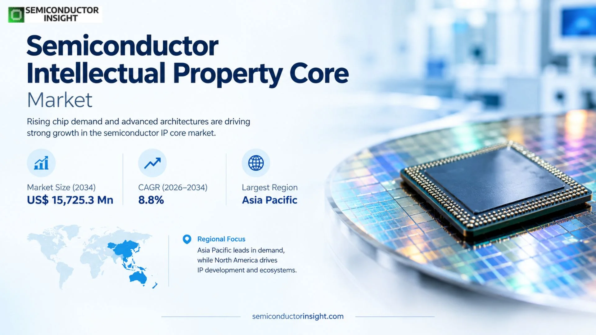
Semiconductor Intellectual Property Core Market is estimated at US$ 7,375.1 million in 2025 and is projected to reach US$ 15,725.3 million by 2034, representing an anchor-consistent CAGR of 8.8% during 2026–2034. Asia Pacific is the largest demand market, while North America remains a central IP-development and platform-ecosystem hub.
A semiconductor IP core is a reusable, pre-designed block of logic or circuit functionality licensed for integration into an integrated circuit, system-on-chip or multi-die design. The market includes processor architectures and cores, interface controllers and PHYs, memory-related IP, analog and mixed-signal blocks, security functions and other reusable design assets. The commercial product is therefore not a physical chip alone: it is a combination of design files, verification collateral, documentation, process-porting work, support and licensing rights that lets customers shorten development schedules and reduce duplicated engineering.
The market boundary covers third-party and licensable semiconductor IP used by fabless companies, IDMs, foundries and system OEMs. It excludes general EDA software revenue unless directly tied to IP licensing, and it does not count finished semiconductor devices as IP revenue. This boundary is important because a processor core, PCIe controller or memory interface can be designed once, adapted across process nodes and licensed into many customer products, giving the business model high reuse economics but also significant upfront R&D and verification requirements.
Complexity is the core demand mechanism. Advanced SoCs combine CPU, GPU, NPU, DSP, memory, security, high-speed I/O and domain-specific accelerators under tight power and area constraints. Designing every block internally would lengthen schedules and expand verification risk. Customers therefore buy mature IP where differentiated value does not require proprietary design, reserving internal engineering for system architecture or unique accelerators. The result is a market in which time to silicon, ecosystem compatibility and process qualification can matter as much as the headline performance of the core.
Chiplets are widening the strategic role of IP. The UCIe Consortium continues to develop a standardized die-to-die interface, while Arm, Cadence, Synopsys and foundry ecosystems are building design flows and reusable building blocks for multi-die systems. This changes the monetization opportunity from a core integrated only inside a monolithic SoC to IP that may define chiplet interfaces, memory subsystems, security boundaries and reusable compute tiles. Suppliers with standards participation and foundry-qualified deliverables can therefore capture value across a broader design stack.
Segment Analysis: By Type
By type, the market is segmented into processor IP, interface IP, memory IP and other IP. Processor IP anchors the compute architecture of many SoCs, while interface IP is gaining strategic weight as PCIe, Ethernet, DDR, HBM, UCIe and other high-speed standards evolve rapidly and become harder for every design team to implement independently.
| Type | Commercial role | Market position |
|---|---|---|
| Processor IP | Processor IP includes CPU, GPU, DSP and related programmable compute architectures licensed for integration into SoCs. Customers adopt these cores to gain mature toolchains, software ecosystems, performance validation and a shorter route to a working device. The commercial value extends beyond RTL because compiler support, development tools, safety packages and long-term architectural roadmaps can determine the platform’s viability. | Processor IP remains a major value pool because mobile, embedded, automotive and edge systems require scalable compute architectures. Growth is shifting toward heterogeneous designs where general-purpose cores work with AI or domain-specific accelerators. Suppliers with broad software ecosystems and automotive, security or functional-safety support can defend pricing because switching architectures creates substantial customer migration cost. |
| Interface IP | Interface IP includes controllers and physical-layer blocks for PCIe, Ethernet, USB, DDR, HBM, UCIe and other connectivity standards. Each protocol generation raises speed, signal-integrity and verification complexity, so customers often license proven implementations instead of building them internally. Foundry-specific PHY work, compliance testing and reference flows are important components of the delivered product. | This category is one of the fastest-moving parts of the market because data-center AI, chiplets and advanced memory are increasing bandwidth requirements. Cadence and Synopsys continue to expand foundry-qualified portfolios around HBM, UCIe, PCIe and high-speed Ethernet. Commercial demand is strengthened by the need to reach standards compliance quickly while avoiding costly first-silicon failures. |
| Memory IP | Memory IP covers embedded SRAM, nonvolatile memory technologies, memory controllers and supporting interfaces used to store or move data inside a semiconductor design. The design challenge includes density, power, yield, reliability and process portability. Advanced SoCs often need several memory types, making characterized compilers, controllers and process-specific implementations valuable to teams that cannot justify building each block from first principles. | Memory IP demand is supported by AI, automotive and edge workloads that require more local storage and faster movement between compute and memory. The highest-value opportunities occur when suppliers can pair memory macros with advanced interfaces, error correction, safety and foundry qualification. Process-specific optimization is a barrier to entry because a design that works on one node cannot always be transferred without substantial re-characterization. |
| Other IP | Other IP includes analog, mixed-signal, security, clocking, sensor interfaces and specialized accelerator or subsystem blocks. These functions often sit outside a customer’s core differentiation yet can be difficult to verify, particularly when they interact with analog behavior, power management or cryptographic requirements. Licensing lets customers focus scarce engineering resources on product-specific features while relying on a validated implementation for supporting functions. | The segment is fragmented but commercially attractive because niche IP can command premium pricing when it solves a difficult integration problem. Security IP is becoming more important as chiplets and connected devices create new trust boundaries. Analog and mixed-signal blocks also benefit from process expertise and silicon-proven reuse, although their portability across advanced nodes is typically lower than pure digital RTL. |
Why is interface IP gaining strategic importance?
Bandwidth is increasing faster than most product teams can redesign physical interfaces from scratch. AI accelerators need HBM and high-speed Ethernet, advanced processors require successive PCIe generations, and chiplets depend on reliable die-to-die connectivity such as UCIe. Each transition introduces new signaling, power, compliance and verification challenges. Licensing a silicon-proven controller and PHY can remove months of risk from a program, making interface IP an increasingly valuable schedule-insurance product rather than a peripheral design convenience.
Segment Analysis: By Application
By application, the market covers consumer electronics, telecommunications, automotive, healthcare and industrial applications. Consumer and communications devices create large licensing volumes, while automotive and industrial designs can support higher value per program because safety, reliability, lifecycle and specialized interface requirements increase the qualification burden. In the Semiconductor Intellectual Property Core market, this point influences supplier positioning because customers weigh integration risk, operating continuity, support availability and future roadmap compatibility before committing to a platform for production use.
| Application | Demand characteristics |
|---|---|
| Consumer Electronics | Smartphones, wearables, PCs, smart-home devices and other consumer systems use processor, multimedia, security, memory and interface IP to integrate many functions into power-constrained SoCs. Product cycles are short, making time to market critical. Suppliers with reusable platforms, broad software support and proven low-power implementations can capture recurring design wins across device generations even as individual product ASPs face pressure. |
| Telecommunications | Networking, wireless infrastructure and connectivity devices require high-speed data movement, packet processing, security and specialized DSP functions. Interface IP for Ethernet, PCIe and memory subsystems is particularly important as bandwidth rises. Customers value standards compliance and long product lifecycles, so silicon-proven implementations and access to future protocol roadmaps can materially reduce the cost and risk of each redesign. |
| Automotive | Automotive SoCs integrate compute, graphics, AI, networking, memory and security for ADAS, infotainment, body control and domain architectures. The application values functional safety, long-term support and deterministic operation in addition to raw performance. IP suppliers that can provide ISO 26262-oriented collateral, safety mechanisms and automotive-qualified ecosystem support can participate in higher-value programs with longer production lives than many consumer devices. |
| Healthcare | Medical imaging, diagnostics, monitoring and wearable devices use reusable processor, interface, signal-processing and security IP to reduce design time while meeting low-power and reliability needs. Volumes are smaller than consumer electronics, but product lifecycles are longer and certification changes can be costly. Stable roadmaps and long-term support therefore influence supplier selection alongside technical performance. |
| Industrial Applications | Robotics, factory automation, machine vision, energy systems and edge computing require processor, real-time, security and connectivity IP across a wide range of process nodes. Industrial customers value longevity, deterministic behavior and broad temperature support. The application creates opportunities for suppliers that maintain older-node deliverables while also offering advanced AI and high-speed interface blocks for next-generation edge platforms. |
Regional Analysis
Asia Pacific is the largest market by semiconductor-design and device-demand exposure, while North America remains a major global center for IP ownership, EDA integration and platform development. Europe contributes automotive, industrial and processor-design expertise, and other regions participate through specialized design centers and growing fabless ecosystems. This is commercially relevant to the Semiconductor Intellectual Property Core market because vendor selection is typically linked to system-level performance, long service lives and the cost of changing an established architecture after deployment.
What makes regional leadership different in semiconductor IP?
Unlike a physical component market, regional leadership must distinguish where IP is created from where it is licensed and consumed. North America hosts major IP and EDA suppliers and many large fabless customers, while Asia Pacific combines foundries, device manufacturers, consumer-electronics supply chains and rapidly growing design teams. Europe has strong automotive, industrial and processor-design activity. The result is a globally interdependent market in which a core may be designed in one region, ported to a foundry in another and integrated into a product sold worldwide.
| Region | Position | Growth outlook | Demand profile | Supplier-selection logic |
|---|---|---|---|---|
| Asia Pacific | Largest demand market | High | Foundry, fabless and system-design led | Process-node support, local foundry ecosystems, standards compliance and regional design assistance are decisive. Customers value IP that is already characterized on the process and package architectures used by local manufacturing partners. |
| North America | IP creation leader | High | Platform and advanced-design led | Supplier selection emphasizes architecture, software ecosystem, foundry qualification, advanced-node availability, verification and long-term roadmap. The region contains major IP vendors, EDA providers, hyperscalers and fabless semiconductor developers. |
| Europe | Strategic specialty market | Moderate to high | Automotive, industrial and processor-design led | Functional safety, security, automotive lifecycle support and European processor initiatives shape demand. Foundry portability and compliance with global interface standards remain critical for export-oriented designs. |
| South America | Small | Selective | Design-services and application led | Demand comes from limited fabless, industrial and academic design activity. Access to affordable licensing, training and design support can matter more than the broadest advanced-node portfolio. |
| Middle East & Africa | Emerging | Selective to strong in hubs | Specialized design and investment led | Israel is a major semiconductor-design center, while Gulf technology investment is expanding. Security, AI and connectivity IP can benefit where local design programs have access to global foundries and EDA ecosystems. |
Competitive Landscape
Competition centers on silicon-proven quality, architecture ecosystems, standards leadership and foundry qualification. The strongest suppliers do not sell a single reusable block in isolation; they reduce schedule risk by providing documentation, verification, software, implementation support and process-specific deliverables around the licensed core. This is commercially relevant to the Semiconductor Intellectual Property Core market because vendor selection is typically linked to system-level performance, long service lives and the cost of changing an established architecture after deployment.
Arm occupies a central role in processor IP through a broad architecture ecosystem and extensive software compatibility. Synopsys and Cadence combine large interface, memory, processor and verification IP portfolios with EDA platforms, creating an integrated value proposition for customers who want design flows and reusable blocks qualified together. Imagination, CEVA, VeriSilicon, Rambus, eMemory and other specialists compete through graphics, DSP, AI, memory, security or application-specific expertise.
Foundry relationships are a major competitive asset. Advanced-node customers prefer IP that has been characterized or qualified on a target process because late interface or memory failures can delay a high-cost tape-out. Synopsys and Cadence publicly announce interface and foundation IP availability around leading TSMC and Samsung processes, while foundries maintain broader partner ecosystems. This makes process-porting investment and early access to node data a form of capacity that directly affects market share.
Chiplets are creating a new competitive dimension. UCIe standardization lowers the barrier to interoperable die-to-die communication, but successful multi-die systems still require controllers, PHYs, memory interfaces, security and verification. Arm has advanced its Chiplet System Architecture, and EDA/IP suppliers are organizing partner ecosystems around reusable chiplet building blocks. Vendors that become embedded in these standards and reference flows can capture design wins before final system architecture is frozen.
Commercial models include upfront license fees, per-use or per-unit royalties, subscriptions, support and engineering charges. The mix varies by IP type and customer. High-volume processor architectures can support royalty economics, while specialized physical IP may rely more heavily on license and porting fees. Customers increasingly evaluate total design cost, including verification and schedule risk, so a more expensive proven IP block can be economically preferable to a cheaper core that requires substantial internal validation.
| Competitive tier | Representative companies | Strategic position |
|---|---|---|
| Platform leaders | Arm; Synopsys; Cadence | These companies combine broad IP portfolios with software, EDA, verification or architecture ecosystems. Their competitive advantage comes from customer familiarity, foundry access, standards participation and a large base of silicon-proven implementations. They are positioned to capture multi-block programs where a customer values integrated support more than individual-core price. |
| Specialized processor & multimedia IP | Imagination Technologies; CEVA; VeriSilicon | Specialists compete in graphics, DSP, AI, multimedia and custom SoC capabilities. They can win where application-specific performance, licensing flexibility or alternative architectures matter. The challenge is maintaining software and foundry support across enough nodes to compete with larger platform vendors. |
| Memory, security & interface specialists | Rambus; eMemory Technology; Silicon Image/Lattice; Sonics | These companies target narrower high-value functions such as memory interfaces, embedded nonvolatile memory, connectivity and on-chip interconnect. Niche leadership can produce strong customer stickiness because physical and mixed-signal IP requires process-specific characterization and can be expensive to replace late in a design cycle. |
Companies profiled in the report: ARM Ltd., Synopsys, Imagination Technologies, Cadence, CEVA, VeriSilicon, eMemory Technology, Rambus, Lattice Semiconductor / Silicon Image, Sonics. The result for the Semiconductor Intellectual Property Core market is a preference for solutions that can demonstrate repeatable performance, reliable integration and long-term support while fitting the customer’s capital-spending and technology-refresh cycle.
Production Capacity Analysis
For semiconductor IP, “production capacity” is primarily design, verification and process-porting capacity rather than factory output. The scarce resources are senior architects, analog and physical-design engineers, verification teams, foundry enablement, characterization silicon and the software organization needed to maintain reusable blocks across several standards and process generations. For the Semiconductor Intellectual Property Core market, the commercial implication is shaped by customer qualification, installed-base economics and lifecycle support, so procurement decisions depend on more than a single technical specification or headline price.
IP vendors must fund development before customer volume is known. A new PCIe, UCIe, HBM or processor-generation implementation can require architecture, RTL, analog design, verification, compliance testing, documentation and software work before meaningful licensing revenue arrives. Large vendors can spread this investment across many customers, which creates scale advantages. Smaller suppliers can compete successfully in specialized niches, but each additional process node or standard generation consumes engineering resources that might otherwise support new products.
Foundry enablement creates another capacity layer. Physical IP and memory compilers must be characterized for specific process technologies, while advanced interface PHYs depend on detailed electrical models and package assumptions. Early access to foundry data, test chips and certification flows lets suppliers offer production-ready deliverables sooner. This is why public collaborations between EDA/IP vendors and leading foundries are commercially significant: they indicate that capacity is being invested before customers complete their own tape-outs.
Support capacity also matters because reusable IP does not eliminate integration work. Customers need help with configuration, verification, timing closure, software bring-up, safety documentation and protocol compliance. A vendor that wins more licenses than its field-engineering organization can support risks schedule problems and reputational damage. Scalable documentation, reference designs and automated verification therefore increase effective capacity just as factory automation increases output in a physical manufacturing business.
| Capacity factor | Current structure | Commercial implication |
|---|---|---|
| Architecture & RTL engineering | Processor, interconnect and subsystem IP requires experienced designers who can deliver performance, power and configurability while maintaining compatibility across product generations. Talent is difficult to scale quickly because architectural knowledge and customer-use experience accumulate over years. | Engineering depth determines how many standards, market segments and roadmap generations a vendor can support simultaneously. Large portfolios create cross-selling opportunities but also increase maintenance burden, so platform reuse and disciplined product architecture are important to profitability. |
| Physical IP & foundry qualification | PHYs, memory compilers and analog blocks must be implemented and characterized on specific process technologies. This requires foundry data, silicon validation and close collaboration with EDA flows, package assumptions and compliance environments. | Early qualification can translate into first-mover design wins because customers prefer IP available when a new node opens for production. Delayed porting can exclude a supplier from an entire customer generation even if the underlying architecture is strong. |
| Verification & support | Reusable IP must ship with test environments, documentation, reference flows and technical support. High-speed interfaces and safety-critical processor subsystems can generate substantial integration questions after the license is signed. | Support quality affects renewal, reputation and schedule risk. Vendors that automate compliance testing and provide complete reference flows can support more customers per engineer, improving both effective capacity and gross margin. |
Market Dynamics
Market expansion reflects a structural trade-off: SoCs are becoming more complex while product schedules are not getting longer. Reusable IP solves that mismatch, but the value is tempered by licensing cost, integration effort, security exposure and the need to keep pace with fast-changing standards and process nodes. For the Semiconductor Intellectual Property Core market, the commercial implication is shaped by customer qualification, installed-base economics and lifecycle support, so procurement decisions depend on more than a single technical specification or headline price.
The market’s economics favor blocks that are expensive to recreate but broadly reusable. High-speed PHYs, processor architectures, memory compilers and security subsystems fit that profile because each requires deep expertise and verification. As chiplets separate functions across dies, reusable interfaces and subsystem IP can be monetized across even more designs. However, customers with strategic differentiation may still build selected cores internally, and large semiconductor companies can use their scale to negotiate pricing or develop alternatives. The outcome is a market that grows with complexity but rewards vendors that reduce integration risk, not merely those with the largest catalog.
Market Drivers
Forces supporting demand through 2034
| Driver | Impact | Why it matters |
|---|---|---|
| SoC complexity and shorter schedules | High | More functions must be integrated into each device while product windows remain tight. Licensing validated processor, memory and interface blocks lets design teams allocate scarce engineers to differentiated features and reduces duplicated verification work. |
| AI and high-bandwidth computing | High | AI accelerators and data-center processors require advanced compute, HBM, PCIe, Ethernet, security and die-to-die interfaces. This increases both the number and value of licensed IP blocks inside leading designs. |
| Chiplet adoption and UCIe | High | Standardized die-to-die connectivity expands demand for controllers, PHYs, memory, security and verification IP that can be reused across multi-die systems and packaging platforms. |
| Foundry ecosystem expansion | Medium-High | Advanced foundries increasingly publish qualified IP and EDA partner flows. Customers gain confidence when third-party IP is available early on a target node, improving license conversion and reducing tape-out risk. |
Rising SoC complexity increases the value of reuse
Modern semiconductor products combine more compute engines, interfaces, memory structures and security functions than a single team can efficiently design from first principles. Reusing mature IP compresses development schedules and lets internal engineers focus on product differentiation. The benefit becomes larger at advanced nodes because mask sets and engineering time are expensive. A validated block that reduces the probability of a respin can therefore justify a meaningful license premium.
AI systems require a richer IP stack
AI accelerators do not depend on a single compute core. They require high-bandwidth memory, chip-to-chip links, PCIe, Ethernet, security, clocking and verification around the accelerator itself. This creates a multi-block opportunity for suppliers such as Synopsys and Cadence and expands the role of processor and subsystem vendors. As customers build specialized AI silicon, external IP can cover standardized infrastructure while proprietary engineering remains concentrated in the accelerator architecture.
Chiplets create new reusable interfaces and subsystem boundaries
UCIe and related chiplet ecosystems allow designers to partition systems across several dies, but every partition creates new interface, security, memory-coherency and verification requirements. Standardized die-to-die links increase interoperability while making mature controller and PHY IP more valuable. Vendors that also supply verification and packaging-aware flows can become part of a customer’s architecture before individual chiplets are finalized, increasing cross-sell potential across the whole system.
Advanced-node economics encourage proven IP
At leading nodes, the cost of engineering and mask sets raises the financial impact of a design error. Customers therefore prefer IP that is already characterized on the target foundry process and supported by a verified implementation flow. Public foundry collaborations are commercially important because they reduce uncertainty around timing, signal integrity and manufacturability. This shifts competitive advantage toward vendors with the capital and partnerships to port products early.
Market Restraints
Factors limiting addressable growth
| Restraint | Impact | Why it matters |
|---|---|---|
| Licensing and royalty complexity | Medium-High | Customers must evaluate upfront fees, royalties, field-of-use rights, derivative-work terms and long-term maintenance. Complex commercial structures can delay decisions and encourage large semiconductor companies to develop strategic blocks internally. |
| Integration and verification risk | High | Licensed IP is not automatically plug-and-play. Configuration, timing, power, software and protocol interactions can create substantial engineering work, especially in advanced multi-die systems. |
| Security, export controls and regional fragmentation | Medium-High | IP is strategic technology. Trade restrictions, cybersecurity requirements and localization policy can limit cross-border licensing or require region-specific support and legal structures. |
| Rapid standards and node transitions | Medium | Suppliers must continuously reinvest in new protocol generations and foundry processes. A delayed product can miss the customer design window, while maintaining old versions raises portfolio cost. |
Commercial terms can become a strategic procurement issue
IP contracts define more than price. Customers negotiate which products may use the core, how derivatives are treated, what royalties apply, which foundries or process nodes are covered and how long support continues. Large programs can therefore involve legal and business review as intensive as technical evaluation. Complex terms may slow adoption or encourage customers to internalize high-volume functions when long-term royalty economics appear unfavorable.
Integration risk remains after licensing
A proven core can still fail to meet a customer’s system-level targets if memory architecture, clocks, power domains, software or neighboring blocks interact unexpectedly. High-speed physical interfaces add package and signal-integrity dependencies, while safety-critical systems require additional evidence. Customers therefore spend heavily on verification even when using third-party IP. Vendors that provide comprehensive test environments and reference flows reduce this restraint, but they must invest continually to maintain that advantage.
Geopolitics can fragment a global licensing business
Advanced semiconductor technology is increasingly affected by export controls, national security review and localization policy. IP vendors must determine which customers, destinations and end uses are permitted and may need separate support structures across regions. Customers concerned about future access can seek local alternatives or multi-source architectures. The result is higher legal and engineering overhead and, in some markets, reduced willingness to standardize completely on a foreign IP supplier.
Roadmap speed creates persistent reinvestment pressure
Interface standards, memory technologies and foundry nodes advance on overlapping schedules. A supplier cannot monetize an old PCIe, DDR or UCIe generation indefinitely if customers are designing the next one. At the same time, legacy products still require maintenance. This creates a portfolio-management challenge: vendors need enough scale to fund new development while sustaining mature deliverables. Smaller specialists must choose niches carefully to avoid being spread across too many standards.
Market Opportunities
UCIe and chiplet subsystem IP
The expansion of UCIe gives IP vendors an opportunity to sell die-to-die controllers, PHYs, protocol adaptation, coherency, security and verification blocks into multi-die architectures. Unlike a single monolithic SoC, a chiplet platform can reuse common interfaces across several products and process nodes. Vendors that participate early in standards and partner ecosystems can become default building blocks for customers assembling heterogeneous systems.
AI memory and connectivity interfaces
AI training and inference systems depend on moving enormous volumes of data between accelerators, HBM, CPUs and networks. This creates high-value licensing opportunities in HBM, PCIe, Ethernet, CXL, UCIe and related verification IP. The commercial advantage is strongest for suppliers that offer complete controller-plus-PHY solutions qualified on leading processes, because customers can reduce the number of interfaces they must integrate and validate themselves.
Automotive safety and zonal architectures
Vehicles are consolidating electronic functions into domain and central-compute platforms that require processor, network, memory, security and safety IP. Long automotive product lives support durable licensing and maintenance revenue, while functional-safety requirements raise barriers to entry. Suppliers that provide ISO 26262-oriented packages and automotive-qualified reference flows can translate existing IP into higher-value programs without competing only on peak performance.
Regional design ecosystems and sovereign semiconductor initiatives
Governments and companies are investing in local semiconductor design capability, creating new customers that may prefer reusable IP rather than building foundational architectures internally. India, Europe, China and Middle Eastern technology hubs can expand the addressable customer base. Suppliers that provide training, local technical support and flexible commercialization can win early-stage programs while establishing relationships that persist as regional fabless ecosystems mature.
Supply Chain Analysis
The semiconductor-IP value chain starts with architecture and standards, moves through IP design and verification, then through foundry enablement and customer SoC integration. The final commercial value is realized only when the block reaches silicon successfully, so documentation, compliance, software and technical support are core parts of the supply chain rather than optional after-sales services.
Standards & Architecture
IP Design & Verification
Foundry Enablement & Silicon Validation
Customer Integration & Lifecycle Support
Standards & Architecture
Industry standards bodies, processor-architecture roadmaps and customer requirements define protocol, performance and interoperability targets. UCIe, PCIe, Ethernet and memory standards determine large portions of the interface-IP opportunity. Vendors that participate early can align roadmaps before customers commit designs, reducing the gap between specification release and production-ready IP. The result for the Semiconductor Intellectual Property Core market is a preference for solutions that can demonstrate repeatable performance, reliable integration and long-term support while fitting the customer’s capital-spending and technology-refresh cycle.
IP Design & Verification
IP suppliers create RTL, analog circuitry, firmware, software, test benches and documentation. This is the primary intellectual-value stage because reusable engineering is converted into a product that can serve many customers. Verification intensity is high: a defect replicated across licensees can create large support and reputation costs, so mature suppliers invest heavily in validation before release.
Foundry Enablement & Silicon Validation
Physical IP, memory compilers and high-speed PHYs are ported and characterized on target process nodes. Test chips, EDA certification and package-aware validation translate a generic design into a foundry-ready product. Early node availability can decide competitive outcomes because customers choose IP at architecture freeze, long before volume silicon appears. In the Semiconductor Intellectual Property Core market, this point influences supplier positioning because customers weigh integration risk, operating continuity, support availability and future roadmap compatibility before committing to a platform for production use.
Customer Integration & Lifecycle Support
Fabless companies, IDMs and system OEMs configure IP, integrate it into SoCs or chiplets, complete verification and bring up software. Supplier support continues through tape-out and often after production begins. Successful silicon creates reference credibility and future license opportunities, while long product lifecycles generate maintenance, upgrade and next-generation architecture demand.
Recent Developments
Report Scope & Segmentation
| Attribute | Coverage |
|---|---|
| Market definition | Licensable reusable semiconductor design IP, including processor, interface, memory, analog/mixed-signal, security and related cores supplied with the design, verification, documentation and support collateral needed for customer integration. Finished semiconductor devices and stand-alone EDA software revenue are outside the primary market boundary. |
| By Type | Processor IP (CPU, GPU, DSP and other processor cores); Interface IP (USB, PCIe, Ethernet and other interfaces); Memory IP; Other IP including analog, mixed-signal and specialized functions. Segment naming follows the controlling report page. |
| By Application | Consumer Electronics; Telecommunications; Automotive; Healthcare; Industrial Applications. Each application is assessed according to product cycle, performance, safety, lifecycle and system-integration requirements that affect IP adoption. |
| By End User | Fabless Semiconductor Companies; Integrated Device Manufacturers; Foundries; System OEMs. Commercial models and support requirements differ according to whether the customer integrates IP into merchant semiconductors, captive silicon or foundry enablement platforms. |
| Regions | North America; Europe; Asia Pacific; South America; Middle East & Africa. Regional analysis separates IP-development concentration from licensing demand and customer semiconductor-design activity. |
| Companies | ARM Ltd.; Synopsys; Imagination Technologies; Cadence; CEVA; VeriSilicon; eMemory Technology; Rambus; Lattice Semiconductor / Silicon Image; Sonics. |
Frequently Asked Questions
What is the semiconductor IP core market size in 2025?
The global semiconductor intellectual property core market is estimated at US$ 7,375.1 million in 2025. The market covers reusable processor, interface, memory, analog, mixed-signal, security and related design blocks licensed for integration into SoCs or chiplet systems. Revenue reflects licenses, royalties, support and associated enablement rather than sales of finished semiconductor devices.
What is the projected semiconductor IP core market size by 2034?
The market is projected to reach US$ 15,725.3 million by 2034. Growth is supported by increasing SoC complexity, AI and data-center silicon, advanced automotive electronics, higher-speed interfaces, chiplet architectures and the need to reduce development schedules. Vendors that provide foundry-qualified, silicon-proven IP with strong verification and software support are positioned to capture a disproportionate share of this expansion.
What CAGR is expected during 2026–2034?
The anchor-consistent compound annual growth rate is 8.8% for 2026–2034. The rate is derived from the controlling 2024 and 2032 market-size anchors and then applied consistently to the rebased 2025 and 2034 values. This approach keeps the market-size endpoints and displayed CAGR mathematically aligned throughout the overview. In the Semiconductor Intellectual Property Core market, this point influences supplier positioning because customers weigh integration risk, operating continuity, support availability and future roadmap compatibility before committing to a platform for production use.
Which region is the largest semiconductor IP market?
Asia Pacific is the largest demand market because it combines foundries, fabless semiconductor companies, device manufacturers and large electronics supply chains. Taiwan, South Korea and China are central to manufacturing and foundry enablement, while India is expanding design talent. North America remains a major center of IP creation, platform ecosystems and advanced semiconductor architecture development.
Which IP type has the strongest strategic momentum?
Interface IP has particularly strong strategic momentum because PCIe, Ethernet, DDR, HBM, UCIe and other standards are evolving quickly while bandwidth requirements rise. Customers can reduce schedule and compliance risk by licensing proven controllers and PHYs rather than building every generation internally. Processor and memory IP remain major value pools, especially in AI, automotive and edge-computing designs.
How are chiplets changing the semiconductor IP market?
Chiplets create reusable subsystem boundaries between dies, increasing demand for die-to-die interfaces, memory, security, coherency and verification IP. UCIe provides a common interoperability framework, while Arm, Cadence, Synopsys and foundry ecosystems are building reference architectures and partner programs. This expands IP monetization beyond monolithic SoCs and can make reusable blocks relevant across several process nodes within one system.
Why is foundry qualification important for IP vendors?
A customer wants confidence that physical IP, memory compilers and high-speed interfaces will work on the selected process node and within the intended package environment. Foundry qualification, test silicon and certified EDA flows reduce uncertainty before tape-out. Vendors that complete this work early can win designs before competitors are ready, making foundry relationships a direct source of commercial advantage.
Who are the key companies in the semiconductor IP core market?
Key companies profiled include ARM, Synopsys, Cadence, Imagination Technologies, CEVA, VeriSilicon, eMemory Technology, Rambus, Lattice Semiconductor / Silicon Image and Sonics. Their positions differ by processor architecture, interface technology, memory, graphics, DSP, security and integration support. Competitive strength increasingly depends on ecosystem depth and process qualification rather than a single IP block.
What is the main restraint on semiconductor IP growth?
The main restraints are licensing complexity, integration risk and constant reinvestment in new standards and process nodes. A licensed block still requires system-level verification, while commercial terms can involve royalties, field-of-use restrictions and support obligations. Export controls and regional technology policy can add further complexity. These issues do not eliminate the value of reuse, but they raise procurement and engineering diligence.
How does the semiconductor IP supply chain create value?
Value begins with standards and architecture, moves through IP design and verification, then through foundry porting and silicon validation before customer integration. Each stage reduces a different form of risk. The IP vendor captures the strongest economics when it can reuse engineering across many customers while still providing process-specific deliverables, documentation, software and technical support that improve the probability of first-pass silicon success.
View research sources used for this overview.
Research Sources & Evidence Base
- UCIe Consortium. UCIe Specifications, official die-to-die standard specifications and version roadmap
- Arm. Arm Chiplet System Architecture Makes New Strides, official chiplet architecture ecosystem update, January 2025
- Cadence. Cadence Accelerates SoC, 3D-IC and Chiplet Design with Samsung Foundry, foundry-qualified interface and memory IP collaboration, June 2025
- Synopsys. Synopsys and TSMC Usher In Angstrom-Scale Designs, advanced-node EDA and foundation/interface IP enablement, April 2025
- European Commission. Proposal for the Chips Act 2.0, European semiconductor design and strategic-capability policy context, June 2026
Get Sample Report PDF for Exclusive Insights
Report Sample Includes
- Table of Contents
- List of Tables & Figures
- Charts, Research Methodology, and more...
 Download Sample Report PDF