
Key Statistics
Key Takeaways
- 300 mm wafers are the leading wafer-size segment because advanced logic and memory fabs are designed around large-diameter substrates that lower cost per die and support high-volume production.
- Memory remains the largest application because DRAM, NAND and high-bandwidth memory consume large volumes of polished and epitaxial 300 mm wafers; AI infrastructure is reinforcing this requirement even while legacy device demand recovers unevenly.
- Japan remains the largest market in the source page, supported by the headquarters, technology base and production footprint of major silicon suppliers, while China is gaining strategic importance through domestic capacity programs.
- Shipment recovery is real but uneven: SEMI reported 2025 worldwide wafer shipments of 12,973 million square inches, up 5.8% year on year, while revenue declined 1.2%, showing that volume recovery does not automatically translate into pricing recovery.
- Supply concentration is a structural feature: qualification cycles, crystal-growth know-how, polishing quality, defect control and long customer relationships make advanced wafer supply difficult to displace quickly.
Silicon Wafer Market Overview
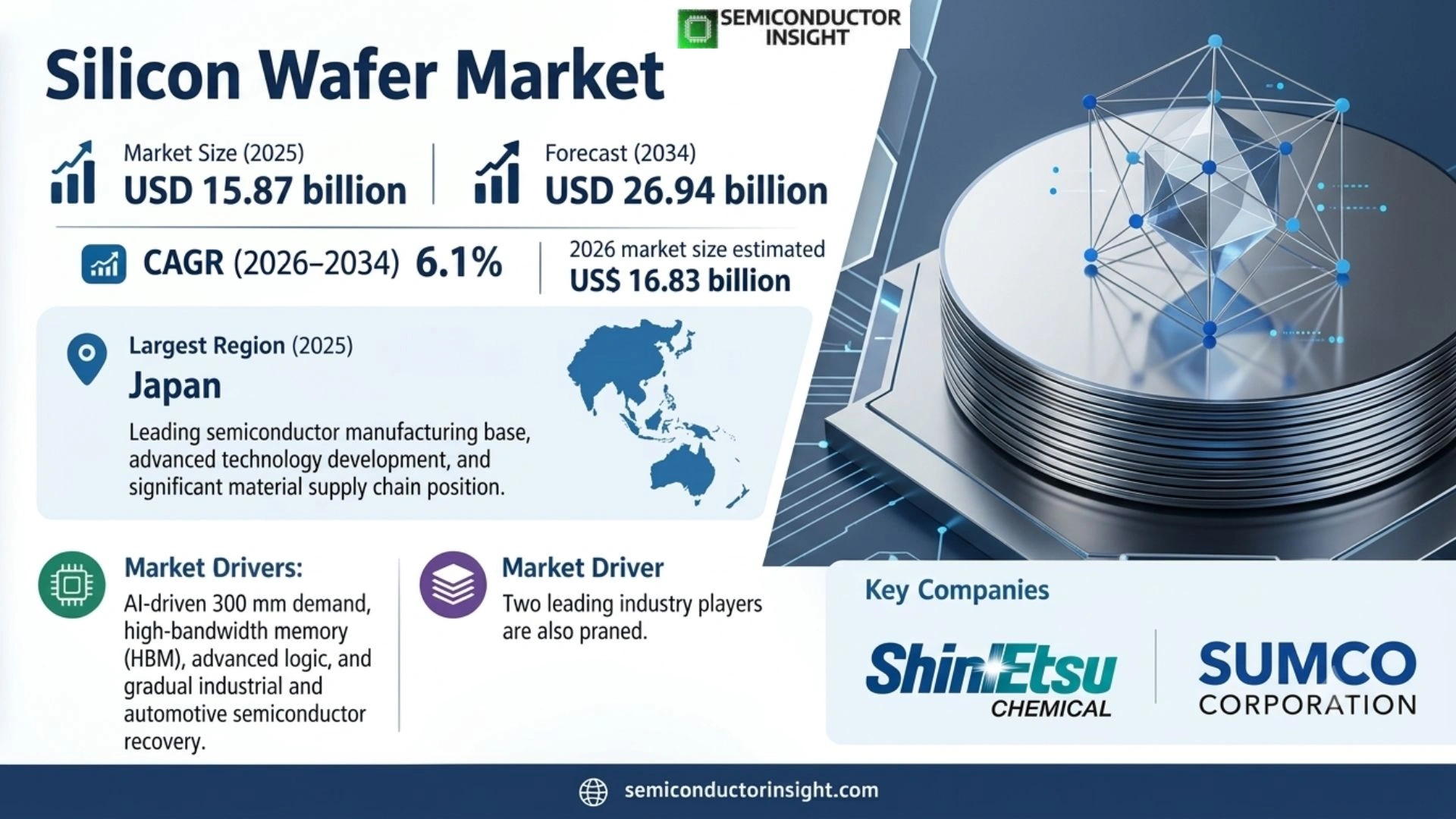
silicon wafer market is rebased to USD 15.87 billion in 2025, rises to an estimated USD 16.83 billion in 2026, and is projected to reach USD 26.94 billion by 2034, representing an anchor-derived CAGR of 6.1% during 2026–2034. Japan is the largest market in 2025, while the growth pattern is being reshaped by AI-driven 300 mm demand, high-bandwidth memory, advanced logic and a gradual recovery in industrial and automotive semiconductor consumption.
Silicon wafers are highly engineered crystalline substrates on which integrated circuits are fabricated. Commercial production begins with semiconductor-grade polysilicon and proceeds through single-crystal growth, ingot shaping, slicing, lapping, etching, polishing and, for many device classes, epitaxial deposition. Buyers do not treat wafers as a commodity input because defectivity, flatness, oxygen content, resistivity, edge geometry and surface preparation directly influence fab yield and device performance.
Demand is linked less to consumer-device unit growth alone than to the number, size and technical intensity of wafers entering fabs. AI accelerators, high-bandwidth memory, advanced logic, power devices and image sensors can pull different wafer specifications even when they share a common silicon base. This makes product mix critical: stronger 300 mm advanced-device demand can coexist with weaker 200 mm and smaller-diameter demand for legacy analog, industrial and automotive applications.
SEMI reported that worldwide silicon wafer shipments reached 12,973 million square inches in 2025, rising 5.8% from 2024, while industry revenue slipped to USD 11.4 billion. The divergence illustrates the core commercial tension in the market: capacity utilization and shipment recovery improve before pricing fully normalizes, particularly when inventories remain elevated in mature-node applications. Suppliers therefore manage capacity additions cautiously and favor long qualification-backed customer relationships.
Segment Analysis: By Type
By wafer size, the source page segments the market into 300 mm wafers, 200 mm wafers, and small-diameter wafers including 100 mm and 150 mm. 300 mm wafers are the leading segment because advanced memory and logic production overwhelmingly uses this diameter, whereas 200 mm and smaller wafers remain essential for analog, power, MEMS, sensor and specialty-device lines whose installed fabs are economically optimized around mature equipment.
| Type | Technical / commercial role | Market position |
|---|---|---|
| 300 mm Wafers | The production standard for high-volume advanced logic and memory. Large surface area increases die output per wafer and supports the economics of leading-edge fabs, but demands exceptional crystal uniformity, polishing control, contamination management and long customer qualification. AI accelerators, cloud processors and HBM are strengthening this segment because their manufacturing ecosystems are concentrated in 300 mm fabs. | Largest and strategically strongest segment. SEMI’s 2025 commentary tied shipment growth particularly to 300 mm demand for advanced logic, cloud infrastructure and memory. Supplier selection emphasizes defectivity, lot consistency, epitaxial capability, reliable volume allocation and the ability to support customer process transitions across multiple technology generations. |
| 200 mm Wafers | A mature but still important platform used extensively for analog, power management, automotive ICs, MEMS, sensors and discrete devices. The economics are driven by fully depreciated fab assets and device designs that do not require leading-edge lithography. Demand is therefore tied to industrial, automotive and consumer cycles rather than the leading-edge AI investment wave. | Stable installed-base segment with cyclical recovery characteristics. Weakness can persist longer than in 300 mm because inventory corrections in analog, industrial and automotive markets reduce fab loading. However, limited availability of mature 200 mm production tools and continued specialty-device demand preserve the commercial relevance of qualified wafer suppliers. |
| 100 mm & 150 mm Wafers | Smaller-diameter substrates serve specialty power, sensor, MEMS, research and legacy process applications where converting a qualified line to larger wafers is uneconomic. These wafers can carry unusual resistivity, orientation or surface specifications and therefore often behave more like engineering materials than standardized high-volume substrates. | Smaller revenue pool but defensible niches. Volume growth is constrained by migration to larger diameters, yet specialty requirements, installed tooling and qualification costs create persistent demand. Suppliers compete on customization, small-lot flexibility and the ability to maintain legacy specifications over long product lifecycles. |
Why does 300 mm remain the commercial center of gravity?
The move to 300 mm is not simply a larger-wafer preference; it is a manufacturing-economics decision embedded in fab design. A 300 mm wafer carries substantially more usable area than a 200 mm wafer, allowing more dies to be processed through a common sequence of deposition, lithography, etch and metrology steps. That advantage becomes most valuable in expensive advanced fabs, which is why leading-edge logic, DRAM and NAND demand has pulled supplier investment toward high-purity 300 mm crystal and epitaxial capacity.
Segment Analysis: By Application
By application, the source page segments demand into Memory, Logic/MPU, Analog, Discrete Device & Sensor, and Others. Memory is the largest application, while logic and high-performance computing are increasingly important growth engines because AI infrastructure requires both advanced processors and large amounts of memory bandwidth. Analog and discrete demand is more closely tied to industrial, automotive and consumer inventory cycles.
| Application | Demand characteristics |
|---|---|
| Memory | DRAM, NAND and HBM production consumes large volumes of 300 mm polished and epitaxial wafers. The commercial trigger is wafer-start demand at memory fabs, which moves with bit growth, inventory levels and technology transitions. AI servers are currently increasing the value of advanced memory content, supporting wafer demand even as commodity memory cycles remain volatile. |
| Logic / MPU | Advanced processors, accelerators and foundry logic use the most demanding 300 mm wafer specifications. Growth is linked to AI, cloud infrastructure, edge compute and leading-node capacity additions. Qualification is stringent because substrate variation can propagate into yield loss across extremely expensive process flows, making quality consistency and secure allocation central purchasing criteria. |
| Analog | Analog ICs often use mature 200 mm and selected 300 mm platforms. Demand follows automotive electrification, industrial automation, power management and consumer electronics, but inventory corrections can be prolonged because analog products have long lifecycles and broad customer bases. Wafer suppliers therefore face more cyclical utilization and price sensitivity than in advanced logic. |
| Discrete Device & Sensor | Power discretes, image sensors, MEMS and other sensor classes use a mix of diameters and tailored wafer properties. The purchasing trigger is application-specific process compatibility rather than diameter alone. Automotive, industrial, mobile imaging and energy systems create resilient demand, but qualification requirements and heterogeneous specifications fragment the supplier opportunity. |
| Others | Specialty devices, research wafers, test wafers and emerging silicon-based photonics applications form a smaller but technically diverse demand pool. Suppliers can earn attractive margins when customers need uncommon resistivity, orientation, epitaxy or surface treatments, although volumes are lower and production scheduling must accommodate smaller customized lots. |
Regional Analysis
The silicon wafer market is structurally concentrated in East Asia because the largest wafer suppliers and many of the world’s highest-volume semiconductor fabs are located there. The source page identifies Japan as the largest market, followed by China, while North America and Europe are strategically important because domestic fab investments are creating new qualification and supply-localization requirements.
How does regional demand differ across the silicon wafer market?
Regional demand follows the physical location and technology mix of wafer fabrication rather than end-device consumption. Japan combines supplier headquarters, crystal-growth expertise and a large specialty-materials base. China is expanding local wafer capability alongside domestic fabs. Taiwan and South Korea pull advanced 300 mm wafers into foundry and memory clusters. North America and Europe are increasing strategic demand through new fabs, but qualification cycles mean local wafer supply develops more slowly than fab announcements.
| Region | Position | Growth outlook | Demand profile | What decides supplier selection |
|---|---|---|---|---|
| Asia Pacific | Largest regional cluster | Highest absolute expansion | Production and fab-led | Long-term qualification, quality consistency, local capacity and allocation security |
| North America | Strategic growth market | High from new fabs | Localization and advanced-node led | Domestic supply resilience, 300 mm capability, technical service and customer qualification |
| Europe | Specialty-focused | Moderate | Automotive, power, industrial and policy-led | Specialty specifications, traceability, quality systems and proximity to European fabs |
| South & Central America | Small | Low to moderate | Import and R&D led | Availability, landed cost and distributor support |
| Middle East & Africa | Emerging | Low from small base | Technology-investment led | Partnerships, imported supply and long-horizon ecosystem development |
Competitive Landscape
Competition is concentrated because advanced silicon wafer manufacturing requires large capital commitments, proprietary crystal-growth and polishing know-how, extremely tight process control and multiyear customer qualifications. The source page names Shin-Etsu Chemical, SUMCO, GlobalWafers, Siltronic and SK Siltron among the major suppliers, with a broader group serving regional and specialty requirements.
The leading suppliers compete less through short-term price discounting than through defect performance, diameter and epitaxy capability, lot-to-lot consistency, customer-specific specifications and assured supply. Once a wafer is qualified into a semiconductor process, switching is costly because a replacement substrate can affect yield across many downstream steps. This creates durable supplier positions but also places heavy obligations on capacity planning and quality assurance.
Japan remains central because Shin-Etsu Chemical and SUMCO have deep expertise in large-diameter silicon and long-standing relationships with global device makers. GlobalWafers, Siltronic and SK Siltron provide alternative large-scale sources across multiple regions, while Wafer Works, NSIG and other Asian suppliers address regional localization strategies. Engineered-substrate specialists such as Soitec participate where SOI or other non-standard structures are required.
The investment cycle is difficult to time. New crystal pulling, slicing, polishing and epitaxial capacity can take years to build and qualify, so suppliers must commit capital before demand is certain. The 2023–2025 downcycle illustrated the risk: industry shipments began recovering before revenue, which means suppliers must balance long-term AI and advanced-node growth against near-term pricing and mature-node utilization.
| Competitive tier | Companies | Why they matter |
|---|---|---|
| Global leaders | Shin-Etsu Chemical; SUMCO; GlobalWafers; Siltronic AG; SK Siltron | These companies possess the scale, 300 mm technology, customer qualifications and multinational supply relationships needed to serve advanced logic and memory fabs. Their strategic advantage is not simply capacity; it is the combination of crystal quality, polishing and epitaxy expertise, reliability records and the ability to support customer ramps across several geographies. |
| Regional / expanding suppliers | Wafer Works; NSIG; Zhonghuan Advanced Semiconductor Materials; Zhejiang Jinruihong; Hangzhou Semiconductor Wafer; GRINM; AST; ESWIN | These suppliers are important to localization strategies, particularly in China and Taiwan, where semiconductor policy and new fab investment encourage domestic sourcing. Their growth opportunity depends on qualifying larger diameters and more demanding specifications while maintaining the cost advantages and responsiveness that regional customers expect. |
| Engineered / specialty | Soitec; FST Corporation | Specialty suppliers address engineered substrates, smaller diameters and tailored material requirements rather than competing only on mainstream polished 300 mm wafers. This creates defensible niches where application-specific performance, wafer structure, orientation or surface preparation matter more than absolute volume. |
Companies profiled in the report
The source page profiles Shin-Etsu Chemical, SUMCO, GlobalWafers, Siltronic AG, SK Siltron, FST Corporation, Wafer Works Corporation, Soitec, National Silicon Industry Group (NSIG), Zhonghuan Advanced Semiconductor Materials, Zhejiang Jinruihong Technologies, Hangzhou Semiconductor Wafer (CCMC), GRINM Semiconductor Materials, Shanghai Advanced Silicon Technology (AST), and Beijing ESWIN Technology Group. The scope retains this full list while competitive tiering distinguishes mainstream large-diameter leaders from regional and engineered-substrate suppliers.
Production Capacity Analysis
Production capacity is concentrated where high-purity polysilicon, crystal-growth expertise, precision slicing and polishing, epitaxial capability, utilities and semiconductor customers coexist. Japan, Taiwan, South Korea, China, Europe and selected North American locations form the core supply network, but not all installed capacity is interchangeable because customers qualify specific wafer types, diameters, plants and process conditions.
The first physical constraint is crystal growth. Producing large-diameter single-crystal silicon with controlled oxygen, carbon, dopant distribution and defect density requires stable furnaces, high-purity feedstock and experienced process control. The second constraint is downstream finishing: slicing, edge shaping, lapping, etching, polishing and cleaning must deliver flatness and surface quality that remain consistent across thousands of wafers. Advanced epitaxial wafers add another capacity layer and can become tight when leading-edge logic or power demand accelerates.
Capacity utilization matters as much as nominal capacity. During a semiconductor correction, customers reduce wafer starts and draw down inventory, leaving suppliers with underused assets that still carry high depreciation and energy costs. When demand returns, utilization can improve quickly, but expanding qualified capacity takes much longer. This asymmetry encourages long-term agreements and staged investments rather than purely spot-market behavior.
SEMI’s 2025 and 2026 shipment data show the market moving from correction toward recovery. 2025 shipments rose to 12,973 MSI, and Q2 2026 shipments reached 3,573 MSI, up 7.4% year on year. The recovery is strongest in AI-related advanced logic and memory, while industrial and automotive markets are only gradually improving, so suppliers must allocate investment by wafer diameter and specification rather than treating demand as a single cycle.
Market Dynamics
The market is being pulled upward by AI-related 300 mm demand and broader semiconductor capacity investment, but the pace is moderated by mature-node inventory cycles, capital intensity and pricing pressure. The most important commercial distinction is between advanced-node wafers, where qualification and supply security dominate, and mature-diameter products, where utilization and customer inventory can create more pronounced price competition.
Market Drivers
| Driver | Directional impact* | Commercial mechanism |
|---|---|---|
| AI, HBM and advanced logic | High | Advanced accelerators, server processors and high-bandwidth memory increase wafer starts on 300 mm platforms and require demanding polished or epitaxial specifications. Because these fabs have high process costs, buyers prioritize yield stability and long-term qualified supply, supporting investment by top-tier wafer producers. |
| New fab construction | High | Government incentives and strategic semiconductor investments are adding fab capacity in the United States, Europe and Asia. Each new fab creates a long qualification pipeline for wafer suppliers and can shift regional sourcing requirements toward diversified or locally supported supply. |
| Automotive and industrial recovery | Medium | Recovery in power management, sensors, analog and discrete semiconductors supports 200 mm and specialty wafers after a prolonged inventory correction. The effect is slower than AI because these markets carry longer inventories and mature product cycles. |
| 300 mm migration | Medium | Larger wafers improve cost per die and are embedded in modern high-volume manufacturing. The migration supports advanced wafer demand, although it simultaneously limits growth in some smaller-diameter categories. |
AI infrastructure expands advanced wafer starts
AI compute growth increases demand for leading-edge processors, HBM and associated logic, all of which rely heavily on advanced 300 mm wafer capacity. SEMI linked the 2025 shipment recovery to advanced epitaxial wafers for logic and polished wafers for HBM. For wafer suppliers, this means the most valuable growth is specification-intensive rather than simply area growth, favoring firms with strong epitaxy, defect control and customer qualification capability.
Global fab investment broadens the customer map
New semiconductor fabs in the United States, Europe, Japan, Korea, Taiwan and China create qualification opportunities for wafer producers. A new fab cannot simply buy any available substrate; it must qualify specific wafer constructions and supplier sites into process recipes. This turns geographic expansion into a multiyear commercial opportunity that rewards early technical engagement and local support rather than late-cycle spot supply.
Automotive electrification supports mature and specialty diameters
Electric vehicles, ADAS, power management and industrial automation consume large quantities of analog, sensor and power semiconductors produced on mature processes. Many of these devices remain economically suited to 200 mm or specialty wafers. As inventories normalize, demand recovery can lift utilization across wafer categories that did not participate fully in the AI-led 300 mm rebound.
Long qualification cycles reinforce incumbent relationships
Semiconductor manufacturers optimize processes around extremely tight substrate specifications, and a change in wafer source can require extensive engineering validation. This creates high switching costs and makes reliable quality performance commercially valuable. Incumbent suppliers that maintain consistency through market downturns are therefore well positioned to capture the next upcycle without competing only on price.
Market Restraints
| Restraint | Directional impact* | Commercial mechanism |
|---|---|---|
| Semiconductor cyclicality | High | Wafer demand changes with fab utilization and customer inventory. When device makers cut wafer starts, substrate suppliers experience rapid utilization declines while carrying fixed costs, producing pricing and margin pressure even when long-term demand remains intact. |
| Capital intensity | Medium to High | Crystal pulling, polishing and epitaxial capacity require expensive specialized equipment, clean manufacturing environments and long qualification cycles. Investment must be committed before demand is visible, increasing the risk of temporary oversupply. |
| Mature-node weakness | Medium | Industrial, automotive and consumer recovery can lag leading-edge AI demand, leaving 200 mm and smaller-diameter lines underutilized. This creates a two-speed market and reduces the benefit of headline shipment growth for suppliers exposed to legacy applications. |
| Geopolitical concentration | Medium | Major wafer production and semiconductor fabrication are concentrated in East Asia. Trade controls, logistics disruption or regional tension can force customers to qualify alternate sources, but diversification itself requires time and capital. |
Inventory corrections can outlast device demand changes
Silicon wafers sit upstream of device inventories, so a customer can reduce wafer starts sharply while continuing to ship finished semiconductors from stock. This lag makes substrate demand more volatile than end-market consumption. The 2024–2025 period demonstrated how mature-node weakness can persist even while AI-related devices expand, complicating capacity planning and reducing pricing power for exposed wafer grades.
Capacity additions have long payback periods
Large-diameter wafer capacity requires crystal pullers, precision finishing equipment, clean utilities and substantial engineering resources. After installation, each production path must be qualified by semiconductor customers. Because the commercial ramp is slower than the construction decision, suppliers risk bringing capacity online during a demand correction. This favors staged expansions and long-term customer commitments but restrains rapid entry by new competitors.
Pricing recovery can lag shipment recovery
SEMI reported that 2025 shipments increased while industry revenue declined, indicating softer average realization and product-mix effects. For suppliers, stronger volume does not guarantee immediate margin recovery when customers retain negotiating leverage or when lower-value mature products remain weak. This dynamic restrains headline revenue growth even as physical wafer area shipped moves upward.
Regional diversification cannot be achieved quickly
Governments and device makers want geographically diversified semiconductor supply chains, but silicon wafers are deeply qualified materials. A new local plant must reproduce the quality and consistency of established sites before customers will use it in critical production. This means localization creates opportunity but also imposes a multiyear technical barrier that can slow the practical reduction of geographic concentration.
Market Opportunities
Advanced epitaxial wafers for AI and high-performance logic
Suppliers that can deliver low-defect epitaxial 300 mm wafers for advanced logic and power applications can capture a higher-value portion of the growth cycle. AI expands both processor and memory requirements, increasing the commercial importance of substrate uniformity, surface quality and epitaxial control. The opportunity is strongest for already qualified suppliers because leading-edge fabs are reluctant to accept process risk from unproven material sources.
Localized supply near new fabs
The expansion of semiconductor manufacturing in the United States, Europe and selected Asian countries creates opportunities for local finishing, epitaxy, inventory hubs and eventually crystal-growth capacity. Wafer suppliers that engage during fab construction can align specifications, qualification schedules and logistics before production ramps, creating long-duration customer relationships and reducing the buyer’s dependence on a single geography.
Specialty wafers for power, sensors and photonics
Not all growth belongs to mainstream polished 300 mm products. Power devices, MEMS, image sensors, silicon photonics and specialty analog applications can require custom resistivity, orientation, epitaxy or engineered substrate structures. These niches offer attractive differentiation because buyers value technical fit and lifecycle support more than lowest unit price, allowing capable suppliers to defend margins despite smaller production volumes.
Recovery in 200 mm automotive and industrial demand
As automotive and industrial semiconductor inventories normalize, wafer starts on mature processes can improve. This creates an opportunity for suppliers with 200 mm and specialty capacity that remained underutilized during the correction. The key is disciplined capacity rather than aggressive expansion: demand recovery can improve utilization and profitability without requiring the same capital intensity as a new advanced 300 mm line.
Supply Chain Analysis
High-purity polysilicon
Crystal growth & ingot preparation
Slicing, polishing & epitaxy
Fab qualification & delivery
High-purity polysilicon
Electronic-grade polysilicon provides the feedstock for single-crystal growth. Purity requirements are far tighter than for solar-grade material because trace contaminants can affect device behavior. Supplier qualification, secure energy supply and chemical purity therefore influence the economics and resilience of the wafer value chain before crystal growth begins.
Crystal growth & ingot preparation
Czochralski or related growth processes convert polysilicon into controlled single-crystal ingots. Diameter, dopant profile, oxygen concentration and defect characteristics are established here, making crystal growth one of the most knowledge-intensive stages. Large-diameter production requires stable equipment, high yields and experienced process engineering.
Slicing, polishing & epitaxy
Ingots are sliced into wafers, then lapped, etched, edge-shaped, polished and cleaned to meet strict geometric and surface requirements. Some products receive epitaxial layers. This stage captures substantial value because downstream fab yield depends on flatness, particles, defects and surface chemistry, while equipment and process recipes are highly specialized.
Fab qualification & delivery
Finished wafers are qualified at semiconductor fabs and supplied under controlled logistics. Customers often approve specific plants, wafer recipes and inspection criteria. Once qualified, supplier relationships become sticky, but service expectations are high: lot traceability, consistent delivery and rapid technical support are essential because a substrate issue can disrupt an entire fabrication line.
Recent Developments
Recent market developments show a transition from correction toward differentiated recovery, with AI-related 300 mm demand leading while mature applications normalize more slowly. The most relevant events are not only supplier announcements but also industry shipment data because they reveal whether physical wafer starts and pricing are recovering together.
July 2026 — worldwide silicon wafer shipments accelerated
SEMI reported Q2 2026 shipments of 3,573 million square inches, up 7.4% year on year and 9.1% sequentially. The organization attributed growth to AI demand expanding beyond advanced logic and memory into power devices and photonics, while industrial and automotive markets showed signs of recovery. This broadening improves the demand mix for suppliers with both 300 mm and specialty portfolios.
February 2026 — 2025 industry shipment results confirmed the rebound
SEMI reported 2025 worldwide silicon wafer shipments of 12,973 million square inches, up 5.8%, while revenue declined 1.2% to USD 11.4 billion. The combination shows that shipment recovery preceded pricing recovery, an important signal for capacity utilization and margins. AI-related demand for advanced epitaxial and polished wafers was the principal positive driver.
October 2025 — SEMI forecast a new shipment record by 2028
SEMI projected silicon wafer shipments to rise from 12,824 MSI in 2025 to 15,485 MSI in 2028, with AI’s expanding compute footprint supporting advanced logic and memory demand. The forecast matters commercially because it supports multi-year capacity planning while still requiring suppliers to distinguish between advanced 300 mm strength and the more gradual recovery of non-AI applications.
Report Scope & Segmentation
| Attribute | Coverage |
|---|---|
| Market | Silicon Wafer |
| Base Year | 2025 |
| Estimated Year | 2026 |
| Forecast Period | 2026–2034 |
| 2025 Market Size | USD 15.87 billion |
| 2034 Forecast Size | USD 26.94 billion |
| CAGR | 6.1% (2026–2034) |
| Largest Market in 2025 | Japan |
| By Type | 300mm Wafers; 200mm Wafers; Small Diameter Wafers (100mm, 150mm) |
| By Application | Memory; Logic/MPU; Analog; Discrete Device & Sensor; Others |
| Regions | North America; Europe; Asia Pacific; South & Central America; Middle East & Africa |
| Companies Profiled | Shin-Etsu Chemical; SUMCO; GlobalWafers; Siltronic AG; SK Siltron; FST Corporation; Wafer Works Corporation; Soitec; National Silicon Industry Group (NSIG); Zhonghuan Advanced Semiconductor Materials; Zhejiang Jinruihong Technologies; Hangzhou Semiconductor Wafer (CCMC); GRINM Semiconductor Materials; Shanghai Advanced Silicon Technology (AST); Beijing ESWIN Technology Group |
Frequently Asked Questions
What is the silicon wafer market size in 2025?
Using the source page’s published anchors of USD 14.96 billion in 2024 and USD 23.95 billion in 2032, the series rebases to approximately USD 15.87 billion in 2025. The same anchor-implied growth factor produces an estimated USD 16.83 billion in 2026 and a projected USD 26.94 billion in 2034, keeping the article internally consistent across the target forecast window.
What is the projected silicon wafer market size by 2034?
The rebased 2034 market size is approximately USD 26.94 billion. This value is derived directly from the source page’s 2024 and 2032 market-size anchors rather than from its printed CAGR label, ensuring that the forecast endpoint and CAGR are mathematically consistent with the published size series.
What CAGR is used for 2026–2034?
The anchor-derived CAGR used for 2026–2034 is 6.1%. The source page prints a higher percentage, but its own 2024 value of USD 14.96 billion and 2032 value of USD 23.95 billion imply an annual growth factor of roughly 6.06%. Under the required workflow, the size anchors control when the printed CAGR conflicts with them.
Which wafer size is the largest segment?
300 mm wafers are the largest segment because advanced memory and logic fabs are built around large-diameter manufacturing. The format improves die output per processed wafer and supports the economics of expensive advanced production lines. AI accelerators, cloud processors, DRAM, NAND and HBM reinforce the segment’s position, while 200 mm remains important for mature analog, automotive and specialty devices.
Which application consumes the most silicon wafers?
Memory is the largest application in the source page, reflecting the scale of DRAM, NAND and increasingly HBM production. Memory fabs consume large volumes of 300 mm substrates and respond strongly to data-center and AI investment. Logic/MPU is also strategically important because leading-edge processors and accelerators require demanding wafer specifications and high-quality epitaxial capability.
Which region is the largest silicon wafer market?
The source page identifies Japan as the largest silicon wafer market and attributes a substantial share to the country. Japan’s position is supported by major suppliers such as Shin-Etsu Chemical and SUMCO, deep crystal-growth and polishing expertise, and long-standing relationships with global semiconductor manufacturers. Asia Pacific more broadly is the world’s dominant production and fabrication cluster.
What is driving current silicon wafer demand?
The strongest current driver is AI-related semiconductor production, especially advanced logic and high-bandwidth memory. SEMI also reports gradual recovery in industrial and automotive applications. New fab construction, 300 mm migration and supply-chain localization provide additional long-term demand, but the recovery remains uneven across wafer diameters and end markets.
What is the main restraint on the market?
Semiconductor cyclicality is the most important restraint because wafer suppliers sit upstream of device inventories. When customers reduce fab utilization, wafer orders can fall quickly even if final electronics demand declines only modestly. High fixed costs, long qualification cycles and delayed pricing recovery amplify the effect, particularly for suppliers exposed to mature 200 mm and smaller-diameter applications.
Who are the major companies in the market?
The source page profiles Shin-Etsu Chemical, SUMCO, GlobalWafers, Siltronic AG, SK Siltron, FST Corporation, Wafer Works Corporation, Soitec, NSIG, Zhonghuan Advanced Semiconductor Materials, Zhejiang Jinruihong Technologies, Hangzhou Semiconductor Wafer, GRINM Semiconductor Materials, Shanghai Advanced Silicon Technology and Beijing ESWIN Technology Group.
What is the most important strategic shift through 2034?
The most important shift is a two-speed market in which AI and advanced 300 mm products grow faster than mature wafer categories, while governments and customers simultaneously seek more geographically resilient supply. Suppliers that combine leading-edge quality, epitaxial capability and qualification depth with regional technical support are positioned to capture higher-value growth without relying solely on commodity wafer volume.

Get Sample Report PDF for Exclusive Insights
Report Sample Includes
- Table of Contents
- List of Tables & Figures
- Charts, Research Methodology, and more...
 Download Sample Report PDF






Be the first to review “Silicon Wafer Market Size, Share, Trends, Market Growth and Business Strategies 2026-2034”