
Key Statistics
Key Takeaways
- Assembly services form the broader revenue pool, while test is becoming strategically more valuable as package complexity rises. Advanced packages require wafer sort, final test, burn-in and system-level test to validate heterogeneous multi-die systems, so the boundary between assembly and test is increasingly an integrated manufacturing flow rather than two independent services purchased solely on unit price.
- Asia Pacific is the largest OSAT region because Taiwan, China, South Korea and Southeast Asia host the densest back-end manufacturing ecosystem. In 2026, ASE expanded high-end packaging and testing capacity in Kaohsiung, Chipbond opened a nearly USD 200 million Penang facility, and KYEC inaugurated a Singapore test operation, demonstrating continued regional capital formation rather than simple installed-base leadership.
- AI and high-performance computing are changing the value mix faster than total market growth. ASE is investing in panel-level packaging, FOCoS, FC-BGA and chiplet integration, while Amkor’s U.S. expansion is explicitly aimed at leading-edge advanced packaging. The opportunity is less about conventional wire-bond volume and more about complex packages with larger substrates, higher I/O density and more test content.
- North America is the most important localization opportunity. The U.S. Department of Commerce awarded Amkor up to USD 407 million toward an approximately USD 2 billion Arizona advanced packaging and test facility, while CHIPS R&D programs committed USD 1.4 billion to advanced packaging research and piloting. This creates a domestic merchant back-end path adjacent to new U.S. front-end fabs.
- Capital intensity, substrate availability, customer qualification and utilization remain key restraints. Amkor spent USD 904.6 million on capital expenditures in 2025, and early-stage Vietnam ramp costs constrained gross margin. Advanced packaging capacity therefore requires more than equipment purchases: OSATs must qualify process flows, build engineering capability, secure substrates and reach sufficient loadings to earn attractive returns.
Outsourced Semiconductor Assembly and Test (OSAT) Market Overview
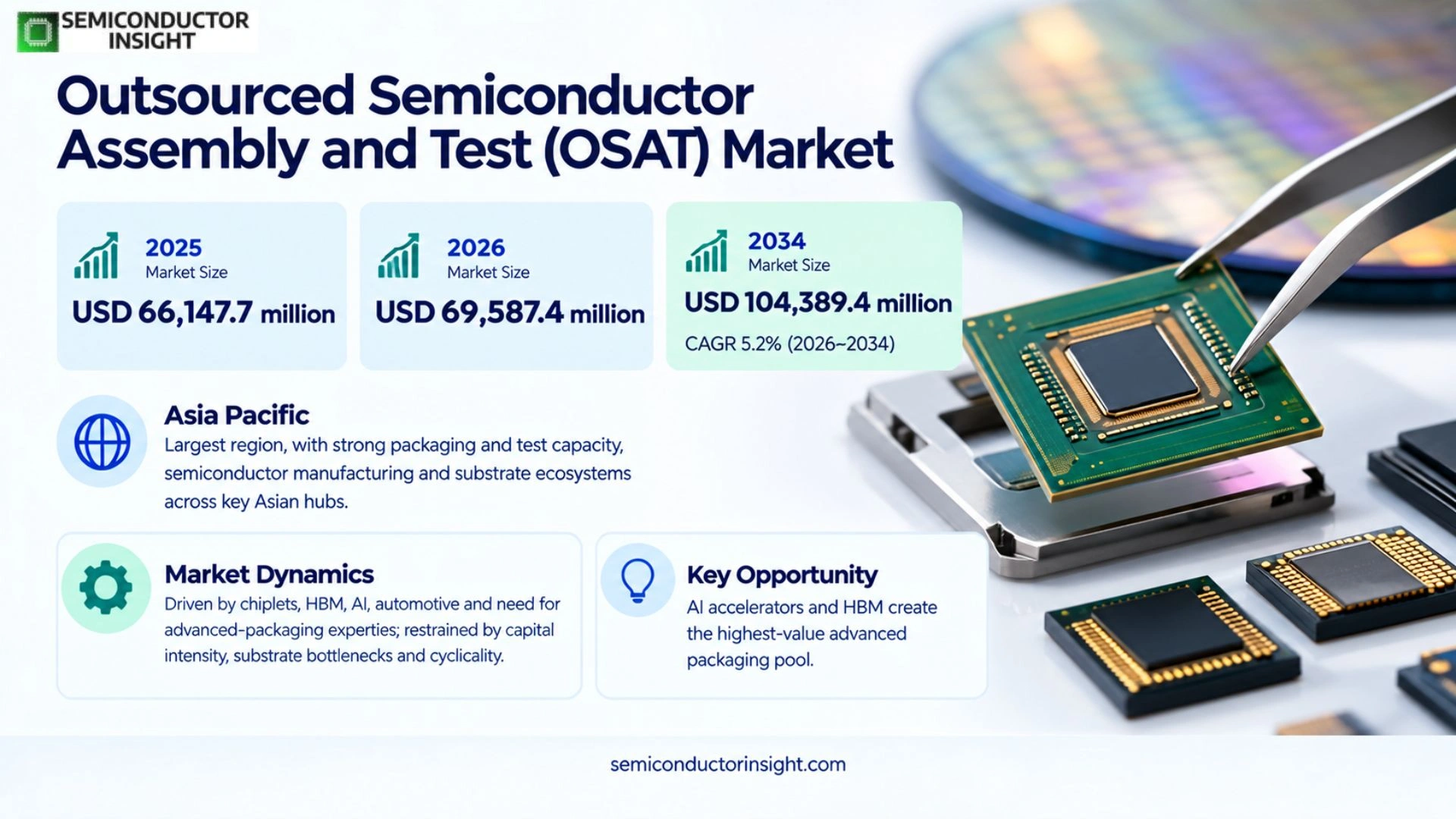
Outsourced Semiconductor Assembly and Test (OSAT) market is estimated at USD 66,147.7 million in 2025 and USD 69,587.4 million in 2026, and is projected to reach USD 104,389.4 million by 2034, expanding at a 5.2% CAGR during 2026–2034. Asia Pacific is the largest region because merchant packaging and test capacity, semiconductor manufacturing, substrate ecosystems and major OSAT headquarters are heavily concentrated across Taiwan, China, South Korea, Malaysia, Singapore and other Asian production hubs.
OSAT providers are merchant semiconductor manufacturers that perform back-end assembly, packaging and testing for fabless chip companies, integrated device manufacturers and foundries. After wafer fabrication, dies must be electrically screened, separated, interconnected, protected and tested in package form before shipment into electronics systems. Conventional services include wafer sort, wire-bond packaging and final test; advanced offerings extend into flip-chip, wafer-level packaging, system-in-package, fan-out, chiplet integration, 2.5D/3D packaging and system-level test.
The market is structurally different from front-end wafer fabrication because customers can outsource varying portions of the back-end flow and can split programs between internal factories, foundry packaging and OSAT partners. The merchant opportunity grows when package complexity outpaces a customer’s internal capability, when new products need rapid capacity without building a captive plant, or when geographic diversification makes a qualified external site more attractive than adding another internal line. This makes engineering responsiveness and qualification speed as important as installed equipment.
Commercial value is shifting toward advanced products. Amkor’s 2025 filing reported USD 6.708 billion of net sales and defined advanced products to include flip-chip, memory and wafer-level processing with related test services. Computing represented 20% of sales, up from 16% in 2023, while communications remained the largest end market at 46%. The mix shows why AI and data-center packaging can lift service value even while mature consumer and smartphone programs continue to supply large baseline volume.
The OSAT market is changing now because chip architecture is changing. Performance improvement increasingly comes from combining multiple dies, high-bandwidth memory and large substrates rather than relying only on transistor scaling. ASE’s automated 310mm × 310mm panel-level platform, Amkor’s Arizona project, Silicon Box’s European panel-level facility and multiple new Asian test investments demonstrate how advanced packaging is becoming strategic manufacturing infrastructure. The resulting market rewards scale, process integration, substrate relationships and customer co-development more than low-cost assembly alone.
Segment Analysis: By Type
By type, the formal source segmentation comprises Test Service and Assembly Service. Assembly services represent the broader physical-manufacturing scope and remain the larger revenue pool, while test services gain strategic importance as advanced packages combine more chiplets, interfaces and high-bandwidth memory. In practice, leading OSATs increasingly sell integrated assembly-and-test solutions because yield learning and final system performance depend on both process flows.
| Type | Service scope | Market position and commercial logic |
|---|---|---|
| Assembly Service | Assembly converts fabricated wafer die into usable semiconductor packages through wafer bumping, redistribution, die attach, wire bonding or flip-chip interconnect, molding, substrate attach, fan-out, system-in-package and increasingly heterogeneous integration. The exact flow varies by product architecture and package platform. | Largest service type. Conventional assembly provides the broad installed revenue base, but value is migrating toward flip-chip, fan-out, FC-BGA, 2.5D/3D and chiplet packages. These formats use larger substrates, finer interconnects and tighter warpage and thermal control. OSATs that can co-design the process with customers capture more engineering value and face higher qualification barriers than commodity package houses. |
| Test Service | Test includes wafer probe or chip probe before assembly, final electrical test after packaging, burn-in for reliability screening and system-level test where devices are exercised under conditions closer to actual use. Test programs require expensive automated test equipment, handlers, sockets, probe cards and application-specific test engineering. | Strategically expanding content. A complex package can contain multiple known-good dies and thousands of interconnects, so a defect discovered late destroys more accumulated value. This increases the economic benefit of early screening, adaptive test and system-level validation. KYEC’s 2026 Singapore site includes chip probe, final test, burn-in and SLT, illustrating the wider test stack demanded by automotive and AI customers. |
How is pricing power shifting within OSAT services?
Commodity package-and-test programs remain price sensitive because customers can benchmark multiple qualified suppliers and utilization strongly affects unit cost. Advanced packaging has different economics: the OSAT contributes process development, package architecture, substrate coordination, thermal and mechanical management, yield learning and specialized test. That engineering content raises switching costs and can support better value capture, but it also requires much larger capital commitments. Suppliers therefore seek programs with customer prequalification, multi-year volume visibility and differentiated technology rather than simply maximizing installed assembly lines.
Segment Analysis: By Application
The source scope segments application demand into Communications, Automotive, Computing, Consumer and Others. Communications remains the broadest volume pool because smartphones and connectivity devices generate enormous package counts, while Computing is the fastest-growing strategic value segment as AI accelerators, CPUs, networking devices and HBM require complex substrates, chiplet integration and intensive test. Automotive adds a second high-value stream through reliability, qualification and long product lifetimes.
| Application | Demand characteristics |
|---|---|
| Communications | Smartphones, tablets, baseband processors, RF components and networking devices create high-volume assembly and test demand. Amkor reported communications at 46% of 2025 net sales, confirming the segment’s scale even as its share has eased from prior years. Buyers emphasize unit economics, very high yield, thin package form factors and rapid product ramps, while premium smartphones increasingly pull advanced wafer-level and system-in-package technologies. |
| Automotive | Automotive demand is driven by ADAS, electrification, infotainment, connectivity and safety electronics. Packaging must survive wider temperature ranges and long qualification cycles, and test coverage is unusually important because field failures can create safety and warranty exposure. New OSAT capacity in Asia and the United States is increasingly designed to support automotive alongside AI, making the segment attractive for suppliers that can combine volume with automotive-grade process control. |
| Computing | Fastest-growing strategic value pool. AI accelerators, CPUs, GPUs, networking ASICs, HBM and data-center devices require advanced substrates, large package bodies, chiplet integration and sophisticated thermal and electrical performance. Amkor’s computing share rose to 20% of 2025 sales from 16% in 2023, while ASE’s 2026 investments explicitly target AI and HPC. Revenue growth can therefore exceed unit growth because package complexity and test content rise sharply. |
| Consumer | Gaming, wearables, connected-home devices, cameras and other consumer electronics create diverse package requirements with high cost sensitivity and shorter product cycles. Amkor reported consumer at 15% of 2025 sales. Suppliers compete on flexible capacity and rapid engineering turns because individual programs can ramp quickly and decline just as fast, limiting the willingness to dedicate expensive advanced equipment without cross-program reuse. |
| Others | The residual segment includes industrial, medical, aerospace, defense and specialized semiconductor applications. Volumes are generally lower but qualification and reliability requirements can be high, supporting specialized packaging and test economics. Regional localization is particularly relevant where governments or customers require trusted manufacturing, traceability or supply continuity, so OSATs with sites in multiple jurisdictions can win programs that would not be awarded purely on lowest manufacturing cost. |
Regional Analysis
Asia Pacific dominates the OSAT market because merchant assembly and test capacity, packaging substrates, semiconductor fabs and major suppliers are concentrated in Taiwan, China, South Korea and Southeast Asia. North America is the most important localization growth opportunity, Europe is building a smaller strategic advanced-packaging base, and South America plus the Middle East & Africa remain emerging ecosystems with limited current merchant capacity.
How does regional competition differ across the OSAT market?
OSAT geography is determined by both labor-and-scale economics and the need to sit close to wafer fabs, substrate suppliers and engineering customers. Asia Pacific wins on ecosystem density and accumulated manufacturing learning. North America is prioritizing trusted advanced packaging adjacent to new domestic fabs. Europe is creating first-of-a-kind chiplet and panel-level capability under the Chips Act. South America is policy-led and import dependent, while the Middle East and Africa are building semiconductor talent and investment foundations rather than operating large merchant back-end clusters today.
| Region | Position | Growth outlook | Demand profile | What decides supplier selection |
|---|---|---|---|---|
| Asia Pacific | Largest | Highest absolute capacity additions | Scale + advanced packaging + test | Technology breadth, cost, substrate access, engineering depth, high utilization, proximity to fabs and customer headquarters, and the ability to ramp AI, communications and automotive packages in high volume. |
| North America | Large demand, smaller merchant production base | Fastest localization opportunity | CHIPS-backed advanced packaging | Trusted domestic capacity, leading-edge package capability, proximity to U.S. fab and design clusters, customer qualification, workforce availability and the ability to integrate advanced substrates, chiplets, HBM and system-level test. |
| Europe | Smaller but strategic | Moderate, policy-supported | Automotive/industrial + chiplet localization | Automotive qualification, regional resilience, Chips Act support, panel-level and heterogeneous-integration capability, traceability and the ability to serve long-lived industrial programs economically. |
| South America | Small | Emerging from low base | Import-dependent electronics ecosystem | Landed cost, customer support, whether Brazil’s industrial policy creates enough local semiconductor manufacturing to justify direct package-and-test investment, and access to qualified global OSAT sites. |
| Middle East & Africa | Nascent | Long-term ecosystem opportunity | Design, AI and capability-building | Government-backed semiconductor strategy, anchor customers, engineering talent, trusted manufacturing requirements and actual wafer-fab or package demand rather than downstream electronics consumption alone. |
Competitive Landscape
OSAT competition is stratified by technology, customer qualification and geography. The largest suppliers can serve everything from high-volume conventional packages to advanced flip-chip, fan-out, system-in-package and heterogeneous integration, while test specialists and regional players compete in narrower service sets. AI is widening the gap because complex packages require co-design, substrates, thermal control and very large capital programs that smaller providers cannot easily replicate.
ASE and Amkor anchor the global merchant advanced-packaging tier, supported by extensive customer relationships and multi-country manufacturing. ASE’s 2026 project pipeline spans high-end packaging, testing clusters and panel-level technology in Taiwan. Amkor is simultaneously ramping Vietnam and constructing Arizona while investing heavily in advanced equipment. Their competitive advantage comes from being able to accept large customer programs, co-engineer package architecture, finance capacity before full utilization and offer geographic diversification across major semiconductor regions.
The second competitive layer includes large Asian OSAT and test specialists such as the source page’s JECT label, Powertech Technology, TSHT, TFME, UTAC, Chipbond, ChipMOS and KYEC. These firms can be highly competitive in memory, display-driver, mixed-signal, automotive or test-intensive programs without matching the complete technology breadth of the largest two. New facilities in Malaysia and Singapore show that regional specialists are also using geographic diversification to deepen customer relationships and reduce concentration risk.
Ownership and naming matter when interpreting source lists. The source page separately includes ASE Group and SPIL even though Siliconware Precision Industries operates within ASE Technology Holding, so they should not be treated as fully independent corporate competitors for concentration analysis. It also lists “JECT,” while the widely recognized Chinese OSAT group is JCET. The formal list is preserved exactly in the report scope, but the reviewer should correct that apparent source-page naming error before publication if the client database requires canonical company names.
Advanced packaging is becoming the primary axis of differentiation. Conventional wire-bond and mature package services remain important for volume, but AI packages increasingly need chiplets, HBM integration, FC-BGA substrates, fine redistribution, large interposers, fan-out and system-level test. ASE’s 310mm panel program is an example of an OSAT trying to change the manufacturing cost curve rather than simply add more conventional equipment. This favors companies that combine R&D, process integration and equipment scale with high utilization.
| Competitive tier | Representative participants | What differentiates the tier |
|---|---|---|
| Tier 1 – global advanced OSAT platforms | ASE Group / SPIL; Amkor | Broad assembly and test portfolios, advanced packaging R&D, multinational capacity, major fabless and IDM qualifications, ability to finance billion-dollar expansions, and engineering resources for chiplet, HBM, fan-out and high-end substrate programs. |
| Tier 2 – large Asian OSAT / test specialists | JECT as listed by the source page; Powertech Technology Inc; TSHT; TFME; UTAC; Chipbond; ChipMOS; KYEC; Unisem | Strong regional scale or specialization in memory, display, test, automotive and mixed-signal applications. Competitive positioning depends on cost, utilization, specific package platforms, customer concentration and the ability to expand geographically without losing process control. |
| Regional / specialized participants | Walton Advanced Engineering; Signetics; Hana Micron; NEPES | Focused customer, technology or geography positions can support durable niches, particularly where long qualification, memory expertise or local relationships matter. The main strategic challenge is keeping equipment and process capability current as customers migrate toward more capital-intensive advanced packages. |
Companies profiled in the source scope
ASE Group; Amkor; JECT; SPIL; Powertech Technology Inc; TSHT; TFME; UTAC; Chipbond; ChipMOS; KYEC; Unisem; Walton Advanced Engineering; Signetics; Hana Micron; NEPES. These names are reproduced exactly from the client source page. Competitive interpretation should avoid double counting corporate relationships such as ASE and SPIL, and the apparent “JECT” naming issue should be reviewed against the intended JCET entity before database normalization.
Production Capacity Analysis
OSAT capacity is not one interchangeable pool. A wire-bond line, wafer-level fan-out line, FC-BGA assembly cell, HBM package flow and automotive test floor require different equipment, substrates, engineering and qualifications. Capacity therefore needs to be measured by process platform and customer readiness rather than square meters alone. The most valuable new investments are those aligned with customer roadmaps and capable of reaching high utilization after qualification.
Asia Pacific remains the center of merchant production because decades of front-end manufacturing, substrates, leadframes, equipment service and electronics assembly created a self-reinforcing back-end cluster. Taiwan is particularly strong in advanced packaging and test, Malaysia in diversified assembly and test, and Singapore in high-value manufacturing and testing. Vietnam is also becoming more important as Amkor ramps a large facility, allowing customers to diversify within Asia while preserving relatively short supply lines to regional wafer fabs.
Advanced packaging changes the physical bottlenecks. Capacity can be constrained by FC-BGA and other substrates, high-end bumping, redistribution-line capability, bonding and molding equipment, warpage control, thermal materials, test sockets and automated test equipment. Large AI packages also need more floor space and longer process flows than simple packages. This means a nominal increase in package units may understate required capital, while a modest number of advanced units can absorb disproportionate equipment and engineering resources.
Customer qualification is a second capacity gate. Package reliability, electrical performance and test coverage must be validated before a customer releases high-volume production. Automotive programs can require especially long qualification and stable process control. For AI packages, co-development begins even earlier because substrate design, chiplet interfaces, thermals and assembly sequence interact. A new plant can therefore be physically complete yet financially underutilized until customer programs pass qualification and ramp.
Capital spending remains substantial. Amkor reported USD 904.6 million of capex in 2025 and said spending focused on advanced packaging and test equipment plus Arizona. ASE has announced multi-billion New Taiwan dollar expansions across Kaohsiung. These projects illustrate the cycle risk: providers must invest before demand is fully realized, but delaying capacity can forfeit strategic programs. Scale leaders manage this through long customer relationships, technology roadmaps and diversified end markets.
Market Dynamics
OSAT growth is supported by chiplets, HBM, AI computing, automotive electronics and customers’ need for external advanced-packaging expertise, while it is restrained by capital intensity, substrate bottlenecks, customer concentration and semiconductor cyclicality. The defining strategic shift is that packaging has become part of system architecture: the OSAT increasingly contributes to performance, not merely protection and final electrical screening.
Market Drivers
| Force | Direction / relative impact* | Evidence-led commercial mechanism |
|---|---|---|
| AI, HBM and heterogeneous integration | High positive | AI processors integrate multiple compute dies, high-bandwidth memory and complex substrates, raising package value and test intensity. ASE, Amkor and Micron investments all show advanced packaging becoming a direct capacity requirement for AI infrastructure. |
| Fabless outsourcing and package specialization | High positive | Fabless companies avoid captive manufacturing and increasingly need specialized package engineering. Even IDMs and foundries outsource portions of back-end flows, expanding the merchant opportunity when OSAT technology is more advanced or flexible than internal capacity. |
| Automotive electronics | Medium-high positive | ADAS, electrification and infotainment increase semiconductor content while demanding stringent reliability and test. Automotive qualification creates switching costs and long program lives, supporting attractive revenue for suppliers with stable processes and geographic continuity. |
| Regional supply-chain localization | Medium-high positive | U.S. and European policy now explicitly supports advanced packaging and test capacity. Localization creates new facilities and second-source qualifications even when total global semiconductor units are unchanged, widening the geographic revenue pool for qualified OSATs. |
AI turns packaging into an architectural performance lever
Traditional scaling cannot economically deliver every performance gain, so designers increasingly combine chiplets, HBM and specialized dies inside one package. That architecture raises the complexity of substrates, interconnect, thermal design and test. ASE’s investments in FOCoS and panel-level processing, along with Amkor’s advanced capacity, show why OSATs are moving upstream into co-engineering. The commercial result is higher content per device and more durable customer integration.
Fabless business models expand the merchant addressable market
A fabless company typically owns product architecture but not high-volume manufacturing infrastructure. As package complexity grows, building a captive back-end line would require specialized engineers, substrate procurement and expensive equipment that may serve only a few product generations. Qualified OSATs spread those assets across multiple customers. This enables faster ramps and turns fixed packaging investment into a variable outsourced service, supporting continued merchant demand even among very large chip designers.
Automotive programs reward process stability and testing depth
Automotive electronics must meet demanding temperature, lifetime and defect-rate expectations. This increases burn-in, electrical screening, traceability and qualification requirements compared with many consumer products. Once a package-and-test flow is approved, customers are less willing to switch solely for a lower price. OSATs with automotive quality systems can therefore earn long program duration, but the initial qualification burden and liability expectations create a meaningful barrier to entry.
Localization creates geographically new revenue pools
The Amkor Arizona project, Silicon Box in Italy and public advanced-packaging research programs show that countries now view back-end manufacturing as part of semiconductor sovereignty. Historically, policy concentrated on front-end fabs while packages still traveled to Asia. The new model seeks more complete regional production. OSATs able to transfer qualified processes across countries can win programs based on trusted supply and proximity even if those plants initially carry a higher cost structure.
Market Restraints
| Force | Direction / relative impact* | Evidence-led commercial mechanism |
|---|---|---|
| Capital intensity and utilization risk | High negative | Advanced packaging equipment and new cleanroom facilities require large up-front spending, while profitability depends on customer qualification and loading. Amkor’s 2025 capex and early Vietnam ramp costs demonstrate how expansion can pressure margins before volume matures. |
| Substrate and material bottlenecks | Medium-high negative | High-end FC-BGA substrates, interposers and specialized materials can constrain package output even when an OSAT has assembly tools available. Large AI packages intensify this exposure because substrate size and layer complexity increase. |
| Customer concentration and cyclicality | Medium negative | Large fabless, IDM and memory customers can shift utilization quickly as inventories change. Capacity dedicated to one package platform or customer may become underloaded, making diversified end markets and reusable equipment important to financial resilience. |
| Technology complexity and talent | Medium-high negative | Chiplet, fan-out, HBM and system-level test require cross-disciplinary expertise in materials, thermals, signal integrity, reliability and yield. Smaller OSATs can struggle to finance both equipment and engineering, widening the capability gap versus global leaders. |
Advanced capacity can be physically installed before it is economically productive
OSAT expansion creates depreciation, staffing and utility costs immediately, but revenue arrives only after process qualification and customer ramps. Amkor said its 2025 gross margin was constrained by the Vietnam facility’s early high-volume manufacturing stage. That example shows why utilization discipline matters: adding capacity too early can dilute margins, while adding it too late can cost an OSAT a strategic customer program. Providers need accurate roadmap visibility and flexible equipment deployment.
Substrate availability can bottleneck the entire package flow
High-performance packages depend on advanced organic substrates, redistribution layers, interposers and other materials whose capacity is concentrated among specialist suppliers. OSATs cannot compensate for a missing substrate by simply running assembly tools faster. As AI packages become larger and more layer-intensive, procurement coordination becomes a strategic capability. Strong OSATs secure material roadmaps with suppliers and customers early, while smaller players can be disadvantaged when allocation tightens.
Customer bargaining power remains substantial in mature services
Large semiconductor companies can qualify multiple OSATs for conventional packages and use competitive bidding to pressure price. Because fixed costs are high, suppliers may accept lower margins to preserve utilization during downturns. This limits pricing power in mature assembly and test despite overall market growth. The defense is differentiation: advanced packages, automotive qualifications, integrated test and co-developed processes are harder to transfer and create more durable customer relationships.
Advanced packaging requires scarce multi-disciplinary engineering talent
Heterogeneous integration brings semiconductor process engineering closer to package design, substrate routing, materials science, thermal management and electrical validation. Recruiting and retaining engineers across all those disciplines is difficult, especially when new plants are built outside established Asian clusters. Governments can fund buildings, but successful OSAT localization also needs process leaders, technicians, suppliers and customer engineering teams. Talent availability can therefore determine ramp speed as much as equipment delivery.
Market Opportunities
AI accelerators and HBM create the highest-value advanced packaging pool
AI systems require large multi-die packages that combine compute chiplets, HBM stacks and sophisticated substrates. Every additional interface increases assembly precision and test complexity, so OSAT revenue per device can rise much faster than semiconductor unit volume. Suppliers that win these programs benefit from long co-development cycles and high switching costs, but they must invest early in bonding, fan-out, FC-BGA, thermal management and system-level test before customer ramps reach peak volume.
Panel-level packaging can improve economics for oversized chiplet packages
ASE’s 310mm × 310mm platform demonstrates an attempt to increase usable processing area and reduce cost per package as chiplet systems become larger. If yields and process uniformity scale successfully, panel-level methods could complement wafer-level packaging for AI and HPC. The opportunity extends to materials, tooling and test as well as assembly. OSATs that establish manufacturable design rules early can influence customer architectures and secure a differentiated position before the technology becomes standardized.
U.S. localization opens premium trusted-manufacturing programs
Amkor’s Arizona facility will sit inside a rapidly expanding U.S. semiconductor cluster. The strongest opportunities are leading-edge AI, high-performance computing, defense and other programs where customers value end-to-end domestic production, engineering proximity or trusted supply. Higher regional costs can be offset when packaging location reduces geopolitical exposure and coordination time. A merchant provider with global process know-how can also transfer lessons from Asian high-volume sites into the new U.S. operation.
Southeast Asia diversification creates capacity without abandoning the Asian ecosystem
Malaysia, Singapore and Vietnam provide customers with new manufacturing locations while preserving access to Asian wafer fabs, substrates and equipment support. Chipbond’s Penang opening, KYEC’s Singapore test site and Amkor’s Vietnam ramp illustrate this pattern. The commercial opportunity is not merely lower cost; it is business-continuity diversification inside a proven semiconductor region. Suppliers that can duplicate quality systems across multiple Asian countries can win second-source and risk-reduction programs.
Supply Chain Analysis
Wafer input and program transfer. The OSAT receives fabricated wafers plus package design, electrical limits and manufacturing requirements from a fabless company, IDM or foundry. Early collaboration is increasingly important because large advanced packages require coordinated die layout, substrate routing and thermal design. The OSAT’s value begins before physical assembly when its process design rules influence whether the customer architecture can be manufactured at target yield and cost.
Wafer-level preparation and known-good-die control. Probe, bumping, redistribution, thinning and singulation determine which die should proceed into expensive advanced packages. The economic logic is critical for chiplets: assembling a defective die alongside several good dies can destroy the value of the whole module. Better pre-assembly screening and traceability therefore reduce downstream scrap and increase the importance of test engineering, data analytics and tight integration between wafer-level and package-level operations.
Assembly and package integration. This stage captures the largest visible share of OSAT manufacturing value and spans commodity wire bond through complex fan-out and chiplet integration. Bottlenecks include high-end substrates, bonding accuracy, molding and warpage control, thermal materials, cleanroom space and qualified equipment. Large AI packages make these constraints more severe because they consume more substrate area, demand more interconnect density and can require process steps not shared with conventional packages.
Final test, system-level validation and delivery. Packaged devices move through final electrical test, reliability screening, burn-in and increasingly system-level test before shipment. Test content rises when devices have more interfaces, higher power and greater functional complexity. KYEC’s new Singapore site illustrates this integrated stack with chip probe, final test, burn-in and SLT. High-quality test protects the enormous value accumulated in an advanced package and can become a separate source of differentiated OSAT revenue.
Recent Developments in the Outsourced Semiconductor Assembly and Test (OSAT) Market
- 26 May 2026 ANNOUNCED
ASE announced development of an automated 310mm × 310mm panel-level packaging line supporting FOCoS and FOCoS-Bridge, with production expected in the first half of 2027. The platform targets AI, HPC and other large multi-die applications and seeks better material utilization than round-wafer processing. The development signals that leading OSATs are redesigning manufacturing formats to address rising package size and cost. Source - 22 May 2026 OPENED
KYEC inaugurated a semiconductor testing facility in Singapore equipped for chip probe, final test, burn-in and system-level test, serving automotive, high-performance AI and 3C products. The investment gives customers another qualified Southeast Asian testing geography and demonstrates that regional diversification is extending beyond assembly into high-value test functions. Source - 8 May 2026 COLLABORATION
ASE and WUS announced an advanced AI packaging hub in Kaohsiung with more than 113,000 square meters of floor area, over 2,000 employment opportunities and completion planned by September 2029. The project targets FOCoS, FC-BGA and related AI/HPC packaging needs, highlighting the increasingly close relationship between OSAT capacity and advanced substrate manufacturing. Source - 11 March 2026 GROUNDBREAKING
ASE broke ground on new high-tech packaging and testing buildings at Nanzih Technology Industrial Park III with a total investment of NT$17.8 billion and completion expected in the second quarter of 2028. The project is designed to add intelligent, integrated logistics, manufacturing and test capacity for AI, HPC and high-speed communications while creating about 1,470 jobs. Source - 9 February 2026 OPENED
Chipbond officially opened a new Penang advanced manufacturing facility representing close to USD 200 million, or roughly RM800 million, of investment. Malaysia’s investment authority described the project as an expansion of the country’s OSAT capacity and ecosystem. The facility strengthens Southeast Asia’s role as a diversification location for packaging and test programs outside the largest Taiwan and China clusters. Source - 16 March 2026 APPROVED
The European Commission granted Open EU Foundry status to Silicon Box’s Novara advanced packaging and testing facility. The plant will integrate chiplets using panel-level packaging, test devices at panel level and is expected to reach full capacity in 2033. The project gives Europe a strategically supported advanced back-end platform for AI, automotive, data-center and supercomputing applications. Source
Report Scope & Segmentation
| Attribute | Scope |
|---|---|
| Market | Global Outsourced Semiconductor Assembly and Test (OSAT) Market. The formal scope covers merchant providers of third-party semiconductor assembly, packaging and test services used by fabless companies, integrated device manufacturers and foundries. It includes conventional and advanced back-end manufacturing where the service is outsourced rather than performed entirely inside the chip owner’s captive operations. |
| Base / Estimated / Forecast | Base year 2025: USD 66,147.7 million. Estimated year 2026: USD 69,587.4 million. Forecast year 2034: USD 104,389.4 million. The resulting 2026–2034 CAGR is 5.2%, derived from the source page’s USD 59,770 million 2023 and USD 94,324.59 million 2032 anchors; the source page’s printed 5.20% agrees with the anchor-implied rate. |
| By Type | Test Service; Assembly Service. The formal scope is preserved exactly from the source page, while descriptive sections explain how modern advanced packaging increasingly integrates wafer-level preparation, assembly and test into a connected manufacturing flow. |
| By Application | Communications; Automotive; Computing; Consumer; Others. Communications remains the broad volume market, while computing is treated as the strongest advanced-packaging growth opportunity because AI accelerators, data-center processors, networking silicon and HBM increase package complexity and test content. |
| Regions | North America; Europe; Asia Pacific; South America; Middle East & Africa. Asia Pacific is the largest market under the source page’s regional analysis; North America is the key localization opportunity, while Europe is adding strategic chiplet and panel-level packaging capacity under the Chips Act. |
| Companies Profiled | ASE Group; Amkor; JECT; SPIL; Powertech Technology Inc; TSHT; TFME; UTAC; Chipbond; ChipMOS; KYEC; Unisem; Walton Advanced Engineering; Signetics; Hana Micron; NEPES. The names are preserved exactly from the client source page even where a naming or corporate-ownership review is required. |
| Customization Scope | Free report customization equivalent to up to four analyst working days with purchase, including addition or alteration of country, regional and segment scope where the requested change remains consistent with the underlying market definition and evidence base. |
Frequently Asked Questions
What is the current size of the global OSAT market?
The global outsourced semiconductor assembly and test market is estimated at USD 66,147.7 million in 2025 and USD 69,587.4 million in 2026. Using the source page’s USD 59,770 million 2023 and USD 94,324.59 million 2032 anchors produces a projected USD 104,389.4 million by 2034 and a 5.2% CAGR during 2026–2034. The calculated rate agrees with the source page’s printed 5.20% CAGR, so no headline growth-rate conflict requires correction.
Which region leads the OSAT market?
Asia Pacific leads because it contains the deepest concentration of merchant assembly and test providers, wafer fabs, packaging substrates, equipment suppliers and semiconductor customers. Taiwan is the advanced-packaging anchor, while China, Malaysia, Singapore, South Korea and Vietnam add large or rapidly expanding back-end capacity. Recent investments by ASE, Chipbond and KYEC show that the region continues to add technology and geographic diversity rather than relying only on its historical installed base.
What services do OSAT companies provide?
OSAT companies provide outsourced semiconductor back-end manufacturing after wafer fabrication. Services can include wafer probe, bumping, redistribution, thinning, singulation, die attach, wire bonding, flip-chip assembly, molding, fan-out, system-in-package, chiplet and 2.5D/3D integration, final electrical test, burn-in and system-level test. The exact service mix differs by supplier and package technology, and leading providers increasingly co-develop process flows with customers rather than merely executing a fixed assembly specification.
Which type is larger: assembly service or test service?
Assembly service is the broader physical-manufacturing category and generally represents the larger revenue pool because it includes the multiple process steps needed to convert die into finished packages. Test service is strategically important and is gaining content as package complexity rises. Advanced chiplet and HBM packages require more screening before assembly and more comprehensive final and system-level test because discovering a defective die late can destroy the value of an entire multi-die module.
Which applications are most important for OSAT providers?
The source scope includes Communications, Automotive, Computing, Consumer and Others. Communications remains a major volume anchor, and Amkor reported that communications represented 46% of its 2025 sales. Computing is the strongest advanced-packaging growth opportunity because AI accelerators, CPUs, networking devices and HBM require large substrates, fine interconnects and complex test. Automotive is also strategically attractive because long qualifications and reliability requirements create durable supplier positions.
Who are the leading OSAT companies?
The client source page identifies ASE Group, Amkor, JECT, SPIL and Powertech Technology among the leading names and also profiles TSHT, TFME, UTAC, Chipbond, ChipMOS, KYEC, Unisem, Walton Advanced Engineering, Signetics, Hana Micron and NEPES. The list needs interpretation: SPIL operates within ASE Technology Holding, so it should not be double-counted as a fully independent group, and the “JECT” label appears to require review against the intended JCET company name.
Why is advanced packaging important to OSAT growth?
Advanced packaging allows semiconductor designers to integrate multiple chiplets, high-bandwidth memory and specialized dies inside one package, improving system performance without relying solely on transistor scaling. That shift raises OSAT content because the package requires more sophisticated substrates, interconnect, thermals, yield control and test. ASE’s panel-level development and Amkor’s advanced expansions demonstrate how packaging has moved from a protective back-end step to an architectural component of AI and high-performance computing systems.
What are the main restraints on the OSAT market?
The major restraints are capital intensity, customer qualification, substrate and material bottlenecks, semiconductor cyclicality and engineering talent requirements. Advanced package lines can cost hundreds of millions or billions of dollars and may operate below efficient utilization during ramp. Amkor reported that early production at its Vietnam facility constrained 2025 gross margin, illustrating how a physically available plant can still depress returns until customer programs, yields and equipment loading mature.
How is semiconductor localization changing OSAT geography?
Governments increasingly treat packaging and test as strategic semiconductor manufacturing rather than assuming wafers can be fabricated domestically and sent abroad for back-end processing. The United States is supporting Amkor Arizona and advanced-packaging pilot infrastructure, while Europe granted Open EU Foundry status to Silicon Box’s Italian packaging and testing facility. Localization therefore creates new qualified production geographies, especially for AI, defense, automotive and other customers that value trusted or resilient end-to-end supply.
What will shape the OSAT market through 2034?
Through 2034, market value will be shaped by AI and HBM package complexity, adoption of chiplets and heterogeneous integration, expansion of automotive electronics, demand for system-level testing, availability of high-end substrates and the pace of regional localization. Asia Pacific should remain the largest manufacturing ecosystem, while U.S. and European advanced-packaging capacity grows from smaller bases. Competitive winners will combine technology breadth, scale, engineering depth, customer qualification and disciplined utilization of expensive new capacity.
Research Sources & Evidence Base

Get Sample Report PDF for Exclusive Insights
Report Sample Includes
- Table of Contents
- List of Tables & Figures
- Charts, Research Methodology, and more...
 Download Sample Report PDF




