Wafer-Level Chip Scale Packaging Market Insights
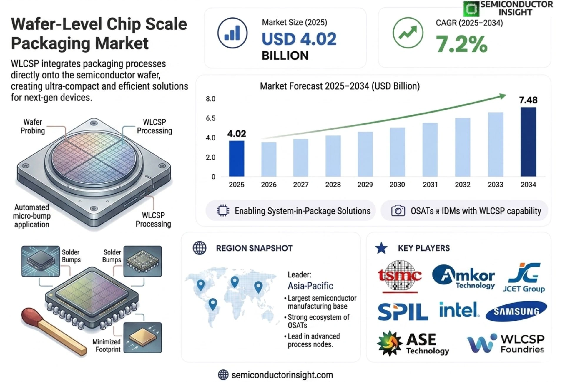
Global Wafer-Level Chip Scale Packaging market size was valued at USD 4.02 billion in 2025. The market is projected to grow from USD 4.02 billion in 2025 to USD 7.48 billion by 2034, exhibiting a CAGR of 7.2% during the forecast period.
Wafer-Level Chip Scale Packaging (WL‑CSP) is a semiconductor packaging technology that integrates the package directly on the wafer surface, delivering chip‑scale dimensions and superior electrical performance through redistribution layers, solder bumping and encapsulation without traditional die singulation.
The market is experiencing rapid growth because demand for miniaturized electronics,especially smartphones, wearables and IoT devices,is soaring; moreover, WL‑CSP offers cost‑efficiency compared with conventional packages. Furthermore, advances in fan‑out wafer‑level techniques and higher I/O density requirements are accelerating adoption. Leading companies such as ASE Technology Holding, Amkor Technology, STATS ChipPAC and JCET are expanding R&D capabilities and production capacity to capture this expanding opportunity.
MARKET DRIVERS
Growing Demand for Miniaturized Devices
Wafer-Level Chip Scale Packaging market is being propelled by the rapid adoption of smartphones, wearables, and IoT sensors, all of which require smaller form factors and higher integration density. Manufacturers are seeking packaging solutions that reduce footprint while maintaining performance, and wafer‑level processes meet those criteria efficiently.
Advancements in Material Technologies
Innovations in low‑k dielectric materials and advanced epoxy molds are enhancing thermal management and mechanical reliability. These material improvements allow designers to push the envelope of power handling and signal integrity, further driving market adoption.
➤ “Wafer‑level packaging enables a 30% reduction in assembly steps, delivering faster time‑to‑market for high‑performance chips.”
Overall, the convergence of device miniaturization trends and material breakthroughs creates a robust growth engine for Wafer-Level Chip Scale Packaging market, positioning it as a preferred choice for next‑generation electronic products.
MARKET CHALLENGES
Complexity of Process Integration
Integrating wafer‑level packaging into existing fab lines demands precise alignment, temperature control, and contamination management. Smaller tolerances increase the risk of yield loss, and many manufacturers lack the in‑house expertise to manage these sophisticated processes.
Other Challenges
Cost Competitiveness
While wafer‑level methods reduce assembly steps, the upfront investment in specialized equipment and material costs can be higher than traditional packaging, deterring cost‑sensitive segments.
MARKET RESTRAINTS
Limited Availability of Skilled Workforce
The specialized nature of wafer‑level processes requires a workforce proficient in both semiconductor fabrication and advanced packaging. The current talent gap slows adoption rates and adds to operational expenditures.
MARKET OPPORTUNITIES
Expansion into Automotive Electronics
As automotive systems move toward higher levels of autonomy, the need for reliable, high‑performance, and space‑efficient packaging grows. Wafer‑level chip scale packaging offers the thermal and electrical characteristics required for power‑train control units and advanced driver‑assistance systems.
Wafer-Level Chip Scale Packaging Market Trends
Rising Demand for Miniaturized Electronics
Wafer-Level Chip Scale Packaging market is being propelled by a pronounced shift toward smaller, lighter electronic devices across consumer and industrial segments. Smartphone manufacturers are prioritizing thinner form factors, while wearables and Internet‑of‑Things sensors require compact footprints without compromising performance. WL‑CSP delivers chip‑scale dimensions that align with these design imperatives, providing superior electrical characteristics and reduced parasitic inductance compared with traditional packages. As manufacturers target higher component density, the ability of wafer‑level processes to embed redistribution layers directly on the wafer simplifies assembly and lowers overall bill of materials. This convergence of size pressure and cost efficiency is creating a sustainable growth trajectory for the market, encouraging both established players and emerging suppliers to expand capacity and refine process yields.
Other Trends
Advancements in Fan‑Out Wafer‑Level Techniques
Recent innovations in fan‑out wafer‑level technology are extending the capabilities of Wafer-Level Chip Scale Packaging market beyond conventional limitations. By redistributing contacts onto a larger substrate area, fan‑out approaches enable higher I/O counts while preserving the benefits of wafer‑level integration. Process refinements such as improved encapsulation materials and precise mold‑compound application are reducing defect rates and enhancing thermal management. These technical gains are attracting high‑performance applications, including automotive radar modules and advanced medical devices, where reliability and signal integrity are paramount. Suppliers are investing in dedicated R&D lines to scale these techniques, thereby strengthening the overall value proposition of wafer‑level solutions in the broader semiconductor ecosystem.
Integration of High‑Density I/O Solutions
The market is also responding to escalating demands for high‑density input/output connectivity. As emerging applications call for more sensors, antennas, and power delivery channels within a single chip, WL‑CSP offers a pathway to meet these requirements without resorting to multi‑chip module architectures. The inherent flexibility of redistribution layers supports fine‑pitch routing, allowing designers to achieve greater functionality per unit area. Consequently, system integrators are favoring wafer‑level packages for next‑generation modules that combine communication, processing, and power management functions. This trend reinforces the strategic importance of wafer‑level packaging in achieving both miniaturization and performance targets across a spectrum of technology domains.
COMPETITIVE LANDSCAPE
Key Industry Players
Global Wafer-Level Chip Scale Packaging Market: Competitive Dynamics, Strategic Positioning, and Leading Manufacturer Profiles
Wafer-Level Chip Scale Packaging (WL-CSP) market is characterized by a moderately consolidated competitive landscape, with a handful of dominant players commanding significant market share while continuously investing in advanced packaging technologies to maintain their edge. ASE Technology Holding Co., Ltd. stands as one of the foremost leaders in the WL-CSP space, leveraging its expansive manufacturing infrastructure, robust R&D pipeline, and strategic partnerships across semiconductor supply chains to deliver high-performance fan-out and fan-in wafer-level packaging solutions. Amkor Technology follows closely, offering a comprehensive portfolio of WL-CSP services tailored to consumer electronics, automotive, and IoT applications. JCET Group and STATS ChipPAC have also established strong footholds by expanding production capacities and advancing redistribution layer technologies to address the rising demand for miniaturized, high I/O density semiconductor packages. The market, valued at USD 4.02 billion in 2025 and projected to reach USD 7.48 billion by 2034 at a CAGR of 7.2%, reflects the intensifying competition among these key players to capitalize on the surging adoption of WL-CSP in smartphones, wearables, and next-generation IoT devices.
Beyond the tier-one leaders, several specialized and regionally prominent companies are actively shaping the competitive contours of the WL-CSP market. Taiwan Semiconductor Manufacturing Company (TSMC) and Samsung Electronics continue to integrate advanced wafer-level packaging capabilities within their broader foundry operations, blurring the lines between chip fabrication and packaging. Powertech Technology Inc. and Tongfu Microelectronics are gaining traction in Asia-Pacific, a region that accounts for the largest share of WL-CSP production and consumption globally. Meanwhile, companies such as Nepes Corporation, Deca Technologies, and Unisem Group are differentiating themselves through proprietary fan-out wafer-level packaging architectures and flexible manufacturing platforms. SFA Semicon and Chipbond Technology Corporation round out the competitive field with niche expertise in bumping, redistribution, and encapsulation processes, catering to the growing requirements of high-volume consumer and industrial semiconductor applications. The competitive intensity is further amplified by ongoing capacity expansions, technology licensing agreements, and cross-border mergers and acquisitions across the global semiconductor packaging ecosystem.
List of Key Wafer-Level Chip Scale Packaging Companies Profiled
- ASE Technology Holding Co., Ltd.
- Amkor Technology, Inc.
- JCET Group Co., Ltd.
- STATS ChipPAC Pte. Ltd.
- Taiwan Semiconductor Manufacturing Company (TSMC)
- Samsung Electronics Co., Ltd.
- Powertech Technology Inc.
- Tongfu Microelectronics Co., Ltd.
- Nepes Corporation
- Deca Technologies Inc.
- Unisem Group
- SFA Semicon Co., Ltd.
- Chipbond Technology Corporation
- Siliconware Precision Industries Co., Ltd. (SPIL)
- Huatian Technology Co., Ltd.
Segment Analysis:
| Segment Category | Sub-Segments | Key Insights |
| By Type |
|
Fan‑Out Wafer‑Level Packaging is emerging as the dominant type because it accommodates higher I/O counts while maintaining a compact footprint.
|
| By Application |
|
Smartphones drive the most compelling demand for wafer‑level CSP because of relentless miniaturization pressure.
|
| By End User |
|
Consumer electronics represent the leading end‑user segment where compact size and energy efficiency are paramount.
|
| By Material |
|
Organic substrate wafers are currently favored for high‑volume consumer applications due to their cost‑effective processing.
|
| By Functionality |
|
High‑frequency RF packages are gaining traction as the leading functional niche.
|
Regional Analysis: Asia-Pacific
The consumer electronics segment represents a significant portion of the Asia-Pacific WCSP market. The increasing demand for smartphones, wearables, and other portable devices with advanced functionalities necessitates smaller and more integrated electronic components. WCSP technology enables the creation of sleeker and more powerful devices, driving its adoption across various consumer electronics manufacturers in the region.
The automotive industry in Asia-Pacific is undergoing a rapid transformation with the increasing integration of electronic systems. From advanced driver-assistance systems (ADAS) to electric vehicle (EV) powertrains, the demand for compact and reliable WCSP solutions is growing substantially. WCSP technology facilitates the integration of sensors, control units, and power management ICs within the automotive electronics, contributing to enhanced vehicle performance and safety.
The expansion of 5G networks and the growth of data centers across Asia-Pacific are driving significant investments in telecommunications infrastructure. WCSP technology plays a crucial role in enabling higher bandwidth, lower latency, and increased energy efficiency in telecom equipment. The compact nature of WCSP allows for better integration of components in dense telecom systems.
The industrial automation and medical device sectors in Asia-Pacific are also witnessing increasing adoption of WCSP technology. The demand for reliable and compact electronic solutions in these applications is boosting the WCSP market. WCSP enables the miniaturization of sensors, control systems, and other critical components in industrial and medical devices.
North America
North America represents a mature market for Wafer-Level Chip Scale Packaging. While the growth rate is relatively steady, the focus is on high-performance applications and advanced technologies. The demand for WCSP in the North American market is driven by the aerospace and defense industries, along with the growing adoption of sophisticated electronic devices in consumer electronics and automotive sectors. Businesses are increasingly prioritizing reliability and security in their WCSP solutions.
Europe
Europe’s WCSP market is characterized by a strong emphasis on innovation and sustainability. The region is witnessing increased adoption of WCSP in automotive electronics, particularly with the rise of electric vehicles and autonomous driving technologies. European manufacturers are also focusing on developing eco-friendly WCSP solutions to meet stringent environmental regulations. The demand for WCSP in industrial automation and consumer electronics remains consistent.
South America
The South American WCSP market is an emerging region with considerable growth potential. The increasing adoption of smartphones, tablets, and other electronic devices is driving demand for WCSP technologies. The automotive sector in countries like Brazil and Argentina is also contributing to WCSP market expansion. However, challenges such as economic fluctuations and infrastructure limitations can impact market growth.
Middle East & Africa
The Middle East & Africa WCSP market is a developing region with promising growth prospects. The expansion of telecommunications networks, particularly in countries like Saudi Arabia and the UAE, is fueling demand for WCSP in telecom equipment. The growing automotive sector and increasing adoption of consumer electronics are also contributing to market growth. Government investments in technology and infrastructure are expected to further boost the WCSP market in the region.
Report Scope
This market research report provides a comprehensive analysis of the Wafer-Level Chip Scale Packaging Market , covering the forecast period 2026–2034. It offers detailed insights into market dynamics, technological advancements, competitive landscape, and key trends shaping the industry.
Key focus areas of the report include:
- Market Overview: The report begins with an overview outlining its current market scenario, key growth indicators, and industry transformation drivers. It discusses macroeconomic factors, demand–supply balance, regulatory landscape, and the strategic role of semiconductors in powering advancements across industries such as automotive, telecommunications, consumer electronics, and industrial automation.
- Market Size & Forecast: Historical data and future projections for revenue, unit shipments, and market value across major regions and segments.
- Segmentation Analysis: Detailed breakdown by product type, technology, application, and end-user industry to identify high-growth segments and investment opportunities.
- Regional Insights: Insights into market performance across North America, Europe, Asia-Pacific, Latin America, and the Middle East & Africa, including country-level analysis where relevant.
- Competitive Landscape: Profiles of leading market participants, including their product offerings, R&D focus, manufacturing capacity, pricing strategies, and recent developments such as mergers, acquisitions, and partnerships.
- Technology Trends & Innovation: Assessment of emerging technologies, integration of AI/IoT, semiconductor design trends, fabrication techniques, and evolving industry standards.
- Market Drivers & Restraints: Evaluation of factors driving market growth along with challenges, supply chain constraints, regulatory issues, and market-entry barriers.
- Stakeholder Insights: Insights for component suppliers, OEMs, system integrators, investors, and policymakers regarding the evolving ecosystem and strategic opportunities.
Primary and secondary research methods are employed, including interviews with industry experts, data from verified sources, and real-time market intelligence to ensure the accuracy and reliability of the insights presented.
FREQUENTLY ASKED QUESTIONS:
What is the current market size of Wafer-Level Chip Scale Packaging Market?
-> Wafer-Level Chip Scale Packaging market size was valued at USD 4.02 billion in 2025. The market is projected to grow from USD 4.02 billion in 2025 to USD 7.48 billion by 2034.
Which key companies operate Wafer-Level Chip Scale Packaging market?
-> Key players include ASE Technology Holding, Amkor Technology, STATS ChipPAC, JCET, among others.
What are the key growth drivers?
-> Key growth drivers include rising demand for miniaturized electronics such as smartphones, wearables and IoT devices, cost‑efficiency of WL‑CSP versus traditional packages, advances in fan‑out wafer‑level techniques, and higher I/O density requirements.
Which region dominates the market?
-> Asia-Pacific leads the market due to a high concentration of semiconductor manufacturers, while North America also shows strong adoption driven by advanced device makers.
What are the emerging trends?
-> Emerging trends include fan‑out wafer‑level packaging, integration of AI/IoT functionalities, use of advanced substrate materials, and increasing focus on sustainability in semiconductor manufacturing.

Get Sample Report PDF for Exclusive Insights
Report Sample Includes
- Table of Contents
- List of Tables & Figures
- Charts, Research Methodology, and more...
 Download Sample Report PDF