Semiconductor Wafer Sorter Market Insights
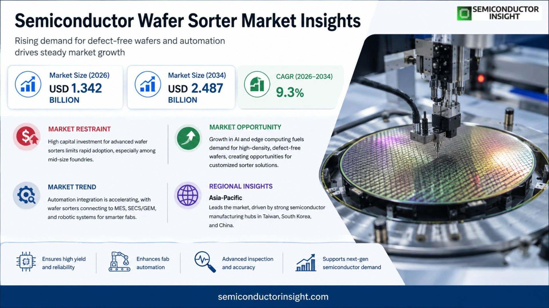
Semiconductor Wafer Sorter market is projected to grow from USD 1.342 billion in 2026 to USD 2.487 billion by 2034, exhibiting a CAGR of 9.3% during the forecast period.
Semiconductor wafer sorters are cleanroom automation systems that connect wafer manufacturing, inspection, logistics and carrier management. Their core role upgrades wafer‑lot handling,from manual or low‑automation processes,to a traceable, programmable and host‑integrated sorting workflow. Official supplier pages show mainstream systems built around wafer identification, pre‑alignment, slot mapping, carrier changeover, lot splitting/merging by ID or rules, wafer flipping and exception checking; high cleanliness and throughput are achieved via OCR, RFID, barcode/WID reading, robotic handling, mini‑environment design and SECS/GEM or GEM300 connectivity together with OHT or AGV interfaces.
The market’s expansion is fueled by rising fab capital expenditures worldwide, regional semiconductor policy incentives and growing demand for advanced nodes such as AI computing and HBM chips. This shift toward platformisation,integrating marking, thickness measurement and inspection,adds value beyond pure mechanical handling. Key vendors including C&D Semiconductor, NADA Technologies, and GL Automation are extending their offerings with modular EFEM‑sorter solutions and long‑term service contracts that reinforce the equipment’s strategic importance within semiconductor factories.
MARKET DRIVERS
Advances in Lithography Equipment Demand
As semiconductor manufacturers pursue sub‑10 nm nodes, the tolerance window for wafer defects narrows dramatically. Precision sorting becomes a prerequisite for maintaining yield, prompting fabs to upgrade to newer wafer sorter generations that can detect sub‑micron anomalies at unprecedented speeds.
Shift Toward Automation in Fab Lines
Automation initiatives are reshaping clean‑room workflows. By embedding wafer sorters within robotic transfer systems, operators reduce manual handling, lower contamination risk, and accelerate throughput. The resulting productivity boost justifies the capital outlay for high‑performance sorting platforms.
➤ “Investors are watching sorter adoption rates as a proxy for fab efficiency gains across the next technology roadmap.”
Collectively, these forces create a virtuous cycle: improved sorting accuracy fuels higher chip yields, which in turn sustains demand for Semiconductor Wafer Sorter Market as manufacturers chase cost‑per‑good reductions.
MARKET CHALLENGES
Integration Complexity with Emerging Node Sizes
Newer process nodes introduce tighter alignment tolerances and unconventional wafer formats. Integrating existing sorter hardware with these specifications often requires extensive software calibration and mechanical retrofits, stretching project timelines and budgets.
Other Challenges
Supply Chain Volatility
Component shortages for high‑precision optics and specialised motors can delay sorter deployments, forcing fabs to rely on legacy equipment longer than planned.
MARKET RESTRAINTS
High Capital Expenditure for State‑of‑the‑Art Sorters
The upfront cost of a modern wafer sorter,often running into several million dollars,poses a significant barrier for mid‑size foundries. While the long‑term ROI can be compelling, the initial financial commitment discourages rapid fleet expansion, especially in regions with tighter capital constraints.
MARKET OPPORTUNITIES
Emerging Applications in AI and Edge Computing
The surge in AI accelerators and edge processors drives demand for wafers with higher transistor density. These product categories place premium importance on defect‑free substrates, opening avenues for sorter vendors to offer customized inspection algorithms and modular upgrades tailored to AI‑focused fabs.
Semiconductor Wafer Sorter Market Trends
Automation Integration Gains Traction
The latest generation of wafer sorters is no longer a stand‑alone mechanical device; it functions as a data‑rich node that synchronises with host MES, SECS/GEM, and robotic logistics layers. By embedding OCR, RFID and barcode readers directly into the transfer station, manufacturers achieve instant lot traceability while preserving the ultra‑clean environment required for 300 mm production. This shift satisfies the need for tighter takt‑time alignment across front‑end and back‑end processes, especially as advanced nodes demand deterministic material flow. Consequently, fab owners prioritize systems that can be programmed through rule‑engine software rather than relying on manual changeovers, a preference that is reshaping procurement specifications across the United States, Japan, South Korea and Taiwan.
Other Trends
Platform Consolidation
Suppliers are blending traditional sorting functions with thickness, weight and defect inspection modules, creating single‑platform solutions that reduce the footprint of material‑handling corridors. The move toward multi‑size compatibility , handling 200 mm, 300 mm and emerging thin‑wafer formats within the same chassis , reflects growing demand from specialty lines such as MEMS and power devices. European vendors, in particular, have leveraged their expertise in glass and thin‑wafer handling to deliver hybrid carriers that support both FOUP/FOSB and open‑cassette types. This convergence lowers capital outlay for fabs that would otherwise need separate equipment for each substrate family, while also simplifying integration with OHT and AGV networks.
Service‑Based Business Models Emerge
Beyond the initial equipment purchase, manufacturers are increasingly monetising software licences, rule‑engine customisation and long‑term maintenance contracts. The recurring revenue stream aligns with fab owners’ preference for predictable total‑cost‑of‑ownership budgeting, especially as the semiconductor ecosystem faces cyclic capital‑spending patterns. Providers that bundle retrofit upgrades , such as adding new wafer‑identification sensors to an existing sorter , gain a competitive edge by extending the useful life of legacy assets. This service orientation also encourages deeper collaboration during project execution, ensuring that hardware, software and factory‑automation layers are delivered as a coherent solution rather than a collection of disparate components.
COMPETITIVE LANDSCAPE
Key Industry Players
Competitive Dynamics in Semiconductor Wafer Sorter Market
The market is currently anchored by a handful of firms that command the bulk of capital equipment contracts for 300 mm and 200 mm fabs. C&D Semiconductor, with its mature portfolio of stand‑alone and EFEM‑integrated sorters, captures a sizeable share of high‑volume foundry projects, thanks to a proven track record of delivering ultra‑clean robotic handling and robust SECS/GEM interfaces. Their ability to marry hardware reliability with customizable rule engines makes them the go‑to supplier for large IDM customers seeking turnkey automation that fits within tight takt times. Parallel to C&D, NADA Technologies leverages deep expertise in thin‑wafer and MEMS handling, differentiating itself through modular architectures that can be retrofitted onto existing carrier platforms. GL Automation’s aggressive expansion into the Asian market,particularly in Taiwan and South Korea,has been driven by aggressive pricing and a service model that bundles spare‑parts logistics with on‑site integration, allowing it to penetrate mid‑size fab lines that value cost efficiency over the absolute highest throughput. Collectively, these leaders shape a tiered competitive structure where top‑tier players focus on large‑scale, high‑value projects, while a second tier of niche specialists targets emerging sub‑segments such as glass‑substrate sorting and multi‑size carrier compatibility.
Beyond the dominant tier, several regionally strong manufacturers contribute to a fragmented yet vibrant ecosystem. European firms like mechatronic systemtechnik gmbh and InnoLas Semiconductor GmbH excel in specialty substrate handling, offering precision thickness and weight discrimination modules that appeal to advanced packaging lines. Asian newcomers,including KoreaTechno Co., Ltd., TIS Co., Ltd., and Shanghai AIXSEMI Semiconductor Technology Co., Ltd.,are rapidly scaling production capacity to satisfy local fab construction programs backed by government incentives. Japanese stalwart Hirata Corporation continues to innovate on mini‑environment designs, while Korean player RORZE SYSTEMS CORPORATION emphasizes AGV‑compatible sorter platforms for smart‑factory deployments. These players, although smaller in revenue terms, intensify competitive pressure by introducing platform‑level modularity and aggressive after‑sales service contracts, forcing the market leaders to augment their value propositions beyond pure equipment sales.
List of Key Semiconductor Wafer Sorter Companies Profiled
- C&D Semiconductor
- NADA Technologies, LLC
- GL Automation, Inc.
- mechatronic systemtechnik gmbh
- InnoLas Semiconductor GmbH
- JEL Corporation
- Hirata Corporation
- SINFONIA TECHNOLOGY CO., LTD.
- NAGASE TECHNO-ENGINEERING CO., LTD.
- KoreaTechno Co., Ltd.
- TIS Co., Ltd.
- RORZE SYSTEMS CORPORATION
- INNOMAX CO., LTD.
- SUN Corporation, Ltd.
- Shuz Tung Machinery Industrial Co., Ltd.
- Shanghai AIXSEMI Semiconductor Technology Co., Ltd.
Segment Analysis:
| Segment Category | Sub-Segments | Key Insights |
| By Type |
|
300 mm Wafer Sorter – Enables high‑throughput handling that matches the rapid takt time of modern 300 mm fabs; – Integrates OCR, RFID and SECS/GEM interfaces to provide end‑to‑end traceability and lot control; – Offers flexible rule‑engine software that can be customized for complex split‑and‑merge operations; – Supports cleanroom mini‑environment designs that preserve wafer integrity while reducing contamination risk; – Provides seamless integration with robotic OHT/AGV logistics, enhancing overall fab material flow. |
| By Application |
|
Wafer Factory – Serves as the central node for lot control in both front‑end and back‑end operations; – Facilitates precise carrier changeover and wafer pre‑alignment, crucial for 300 mm volume fabs; – Enhances throughput by consolidating multiple handling steps (identification, sorting, flipping) into a single platform; – Aligns with advanced packaging workflows, enabling smooth hand‑off to thin‑wafer and MEMS processes; – Provides a programmable interface that supports rapid adaptation to new process recipes and technology nodes. |
| By End User |
|
Foundries – Prioritize wafer sorters that can integrate tightly with high‑volume FOUP logistics and GEM300 standards; – Demand robust, low‑contamination handling to sustain advanced node yields; – Require modular platforms that can evolve with new carrier types and wafer thickness variations; – Value extensive on‑site service and software customization to align with global fab strategies; – Emphasize reliability and uptime, making maintenance contracts a critical selection factor. |
| By Carrier Compatibility |
|
FOUP/FOSB Type – Aligns with the dominant carrier format in leading 300 mm fabs, ensuring seamless hand‑off between lithography and metrology; – Supports high‑speed robotic exchange, reducing wafer dwell time and enhancing overall fab efficiency; – Incorporates RFID and barcode reading for flawless carrier identification and audit trails; – Enables flexible rule‑based sorting that can handle mixed‑size loads within a single FOUP; – Offers a proven reliability track record, making it the preferred choice for both mature and leading‑edge fabs. |
| By Equipment Form Factor |
|
Integrated EFEM/Sorter – Merges wafer handling with front‑end module (EFEM) functions, reducing footprint and simplifying fab layout; – Provides a unified software environment that coordinates inspection, marking and sorting in a single workflow; – Enhances adaptability by supporting multiple carrier interfaces through modular plug‑in cards; – Improves overall equipment effectiveness by eliminating redundant transfer steps; – Positions suppliers as strategic partners, offering end‑to‑end automation solutions that go beyond mechanical handling. |
Regional Analysis: Semiconductor Wafer Sorter Market
Asia‑Pacific
Foundries are scaling line capacities to meet the surge in demand for logic and memory chips. New wafer sorting lines are being added to existing fabs, emphasizing modularity so capacity can be adjusted without prolonged downtime. This trend fuels a steady appetite for next‑generation sorter models that combine throughput with tighter critical‑dimension control.
Partnerships between equipment manufacturers and semiconductor firms have accelerated the rollout of AI‑enhanced inspection algorithms. By embedding machine‑learning on the sorter platform, operators gain real‑time defect classification, reducing reliance on downstream metrology and improving overall yield.
Regional policies prioritizing domestic component sourcing have prompted OEMs to establish assembly lines within the region. Localized supply chains shorten lead times for critical sorter subsystems, allowing fabs to respond faster to production schedule changes.
Energy efficiency and waste reduction have become decisive criteria in equipment selection. Vendors are showcasing low‑power sorter designs that integrate eco‑friendly cooling methods, aligning with corporate sustainability goals and regulatory expectations.
North America
In North America, the emphasis is on integrating wafer sorting with advanced packaging workflows. Leading fabs are retrofitting existing lines to accommodate heterogeneous integration, which demands precise defect detection at smaller feature sizes. The market sees a preference for turnkey solutions that incorporate robust data analytics, enabling manufacturers to blend sorting data with broader factory‑floor intelligence. Competitive pressures from Asian players have urged North American equipment providers to differentiate through after‑sales service and rapid upgrade paths, ensuring that legacy assets remain viable as process nodes shrink.
Europe
European semiconductor hubs, particularly in Germany and the Netherlands, are leveraging the region’s strong engineering base to customize wafer sorter configurations for specialty applications such as power electronics and automotive chips. Regulatory frameworks that stress data security have led to a pull for on‑premise analytics rather than cloud‑based options. Consequently, vendors are tailoring software stacks that meet stringent compliance while delivering the granular defect insight required for high‑reliability products. Collaborative research programs funded by the EU further stimulate innovation in sorter optics and sensor integration.
South America
South America’s semiconductor activity remains modest, yet emerging investment in display and IoT chip fabrication is creating a niche for mid‑range wafer sorting equipment. Local manufacturers prioritize cost‑effective platforms that can be easily maintained with limited technical staff. Partnerships with Asian OEMs facilitate technology transfer, allowing South American fabs to adopt proven sorting architectures without extensive R&D spend. The region’s growth trajectory hinges on expanding domestic supply chains and training programs that build operational expertise.
Middle East & Africa
The Middle East & Africa region is in the early stages of building semiconductor ecosystems, with several governments launching ambitious fab projects. Early adopters are seeking flexible wafer sorter solutions that can be rapidly reconfigured as production ramps up. Because the talent pool is still developing, there is a strong demand for equipment providers to offer comprehensive training and remote diagnostics. These services are becoming a decisive factor in procurement decisions, as they reduce the risk associated with launching new manufacturing capacity.
Report Scope
This market research report provides a comprehensive analysis of the Semiconductor Wafer Sorter Market , covering the forecast period 2026–2034. It offers detailed insights into market dynamics, technological advancements, competitive landscape, and key trends shaping the industry.
Key focus areas of the report include:
- Market Overview: The report begins with an overview outlining its current market scenario, key growth indicators, and industry transformation drivers. It discusses macroeconomic factors, demand–supply balance, regulatory landscape, and the strategic role of semiconductors in powering advancements across industries such as automotive, telecommunications, consumer electronics, and industrial automation.
- Market Size & Forecast: Historical data and future projections for revenue, unit shipments, and market value across major regions and segments.
- Segmentation Analysis: Detailed breakdown by product type, technology, application, and end-user industry to identify high-growth segments and investment opportunities.
- Regional Insights: Insights into market performance across North America, Europe, Asia-Pacific, Latin America, and the Middle East & Africa, including country-level analysis where relevant.
- Competitive Landscape: Profiles of leading market participants, including their product offerings, R&D focus, manufacturing capacity, pricing strategies, and recent developments such as mergers, acquisitions, and partnerships.
- Technology Trends & Innovation: Assessment of emerging technologies, integration of AI/IoT, semiconductor design trends, fabrication techniques, and evolving industry standards.
- Market Drivers & Restraints: Evaluation of factors driving market growth along with challenges, supply chain constraints, regulatory issues, and market-entry barriers.
- Stakeholder Insights: Insights for component suppliers, OEMs, system integrators, investors, and policymakers regarding the evolving ecosystem and strategic opportunities.
Primary and secondary research methods are employed, including interviews with industry experts, data from verified sources, and real-time market intelligence to ensure the accuracy and reliability of the insights presented.
FREQUENTLY ASKED QUESTIONS:
What is the current market size of Semiconductor Wafer Sorter Market?
-> Semiconductor Wafer Sorter market is projected to grow from USD 1.342 billion in 2026 to USD 2.487 billion by 2034, exhibiting a CAGR of 9.3%
Which key companies operate in Semiconductor Wafer Sorter Market?
-> Key players include C&D Semiconductor, NADA Technologies, LLC, GL Automation, Inc., mechatronic systemtechnik gmbh, InnoLas Semiconductor GmbH, JEL Corporation, Hirata Corporation, SINFONIA TECHNOLOGY CO., LTD., NAGASE TECHNO-ENGINEERING CO., LTD., KoreaTechno CO., LTD., TIS Co., Ltd., RORZE SYSTEMS CORPORATION, INNOMAX CO., LTD., SUN Corporation, Ltd., Shuz Tung Machinery Industrial Co., Ltd., Shanghai AIXSEMI Semiconductor Technology Co., Ltd..
What are the key growth drivers?
-> Key growth drivers include increased fab automation investments, expansion of 300mm and specialty fabs, demand for advanced nodes and AI computing, rising need for thin‑wafer, MEMS and glass handling, and strong regional semiconductor policy support.
Which region dominates the market?
-> Asia-Pacific dominates the market, led by Japan, South Korea, Taiwan, and China, while the United States and Europe also hold significant shares.
What are the emerging trends?
-> Emerging trends include greater platform integration (combining marking, thickness, weight discrimination), modular and multi‑carrier architectures, expanded software‑service business models, and enhanced connectivity via OCR, RFID, SECS/GEM, OHT and AGV.

Get Sample Report PDF for Exclusive Insights
Report Sample Includes
- Table of Contents
- List of Tables & Figures
- Charts, Research Methodology, and more...
 Download Sample Report PDF