GaN-On-Si Epiwafer Market Insights
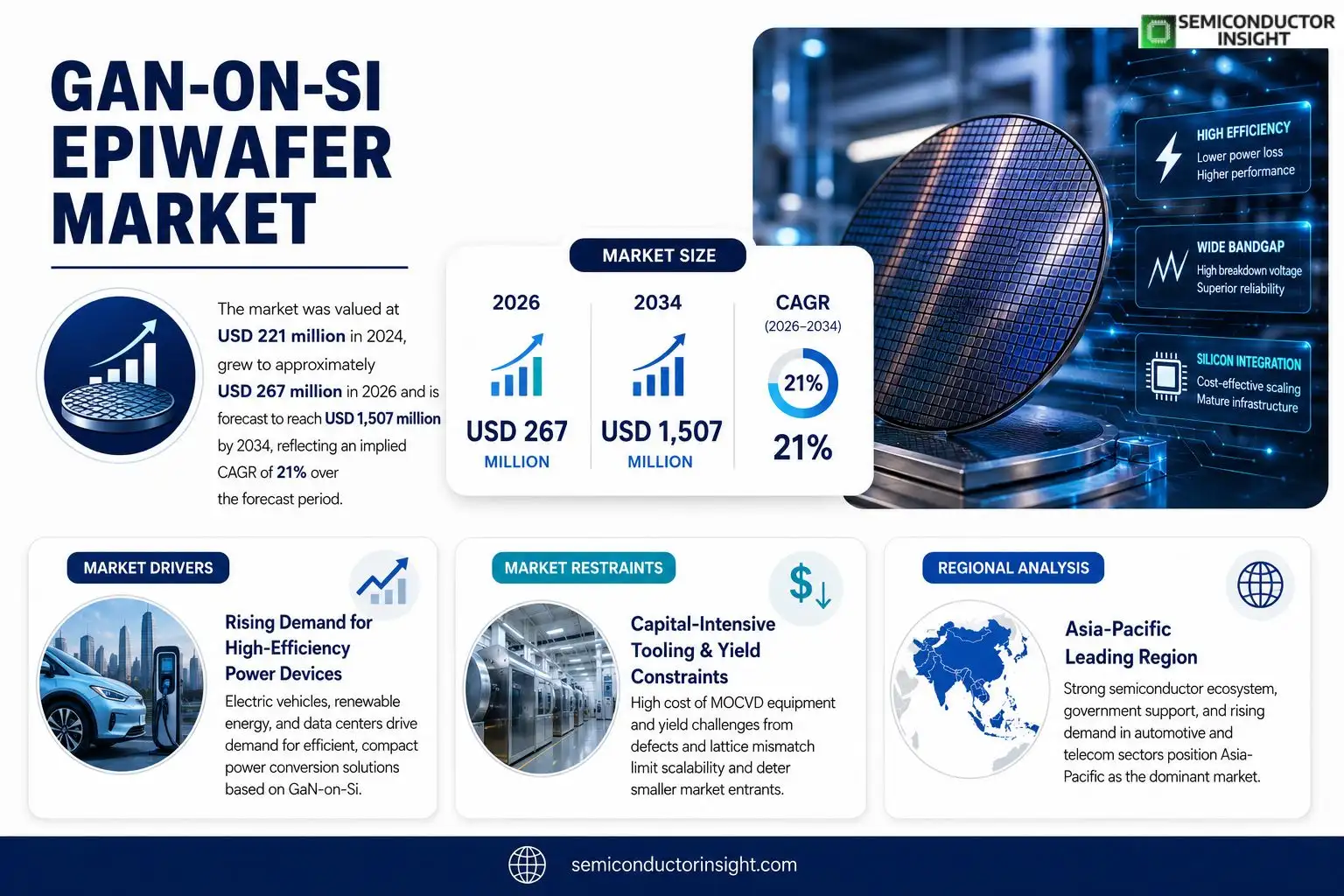
GaN-On-Si Epiwafer market was valued at USD 221 million in 2024, grew to approximately USD 267 million in 2026 and is forecast to reach USD 1,507 million by 2034, reflecting an implied CAGR of about 21 % over the period.
GaN‑On‑Si epiwafers are crystalline gallium‑nitride layers epitaxially grown on silicon substrates, enabling high‑electron‑mobility devices while leveraging mature silicon manufacturing infrastructure.Growth stems from expanding demand for power‑efficient RF amplifiers, automotive power converters and solid‑state lighting; cost advantages of silicon integration encourage adoption even as manufacturers address thermal management and lattice‑mismatch challenges.
MARKET DRIVERS
Rising Demand for High‑Efficiency Power Devices
Automotive manufacturers are transitioning to electric drivetrains that require converters capable of handling higher voltages while minimizing losses. GaN‑On‑Si epiwafer solutions meet these specifications, delivering up to 40 % lower conduction loss compared with traditional silicon devices. This performance edge fuels a surge in volume orders from original equipment manufacturers seeking to meet stricter emissions standards.
Advancements in Substrate Processing
Recent refinements in epitaxial growth techniques have lifted wafer‑size yields from 55 % to above 70 % on 200 mm substrates. The improvement reduces cost per square inch, making the technology financially attractive for mass‑market applications such as data‑center power supplies. Companies that secure these process gains can price competitively against silicon carbide alternatives.
➤ “GaN‑On‑Si platforms now achieve 30 % lower on‑resistance than comparable SiC, reshaping power‑conversion economics.”
As system designers recognize the cost‑performance balance, they are revising bill‑of‑materials to allocate a larger share to GaN‑On‑Si components, a shift that will translate into higher revenue streams for wafer manufacturers in the GaN‑On‑Si epiwafer market.
MARKET CHALLENGES
Manufacturing Yield Constraints
Despite recent gains, defect densities remain a bottleneck for high‑volume production. Even a 1 % increase in dislocation count can erode the cost advantage, prompting fabs to invest heavily in in‑line metrology and defect‑reduction protocols.
Other Challenges
Supply Chain Vulnerabilities
The reliance on high‑purity silicon substrates creates exposure to fluctuations in semiconductor-grade silicon availability, which can delay production schedules and inflate material costs.
MARKET RESTRAINTS
Capital‑Intensive Tooling
Establishing a dedicated GaN‑On‑Si epitaxy line demands multi‑million‑dollar investments in MOCVD reactors and wafer‑handling automation. Smaller players often lack the financial bandwidth to upgrade, limiting market participation and concentrating supply in a few large entities.
MARKET OPPORTUNITIES
Expansion of 5G Base‑Station Power Modules
Deployment of 5G infrastructure escalates the need for compact, high‑frequency amplifiers that operate efficiently at millimeter‑wave bands. GaN‑On‑Si epiwafers, with their superior thermal conductivity and lower insertion loss, are uniquely positioned to satisfy this niche, opening a rapid growth corridor for manufacturers willing to tailor designs for telecom equipment.
GaN-On-Si Epiwafer Market Trends
Accelerating Revenue Expansion
The GaN-On-Si Epiwafer Market recorded revenues of roughly $221 million in 2024. Forecasts indicate a climb to about $826 million by 2031, implying an annual growth rate near 21 percent. This surge reflects the convergence of three forces: the thinning of silicon‑based power device cost structures, increasing adoption of GaN technology in high‑efficiency converters, and a wave of capital spending from automotive and data‑center players seeking lower loss solutions. Companies that have streamlined epitaxial processes are converting the cost advantage into margin improvement, prompting a reallocation of R&D budgets toward larger‑diameter wafers and tighter defect control.
Other Trends
Supply‑Chain Consolidation
Fragmented equipment sourcing historically limited scale for many producers. Over the past two years, several mid‑size fab operators merged with larger silicon substrate firms, creating vertically integrated platforms that can negotiate bulk silicon purchases and lock in critical epitaxy tools. The result is a modest compression of wafer pricing while preserving capacity for niche thickness specifications. Buyers now face a narrower supplier set, which in turn raises the importance of strategic partnership agreements and long‑term price‑escalation clauses.
Application‑Driven Diversification
While power conversion remains the dominant draw, the market is witnessing measurable traction in RF and photo‑electric segments. RF modules for 5G base stations increasingly rely on GaN‑on‑Si substrates to meet high‑frequency performance without the thermal penalties of sapphire. Concurrently, photo‑electric sensors in LiDAR systems are exploiting the material’s high breakdown voltage, offering manufacturers an alternative to costly InP solutions. This broadened addressable base is prompting vendors to introduce 6‑inch and 8‑inch product lines, aligning capacity with the volume needs of automotive radar and telecom equipment manufacturers. As the application mix evolves, firms that can quickly re‑tool their lines to support multiple wafer sizes are positioned to capture incremental revenue streams without sacrificing core profitability.
COMPETITIVE LANDSCAPEKey Industry Players
Competitive Dynamics in the GaN‑On‑Si Epiwafer Segment
Wolfspeed dominates the high‑volume tier of GaN‑On‑Si epiwafer production, leveraging a silicon‑based epitaxy platform that scales to 8‑inch wafers. Its strategic joint‑venture with Taiwan Semiconductor Manufacturing Company has unlocked a supply chain capable of serving both power‑electronics and RF markets. The company’s aggressive capital expenditures, coupled with a portfolio that ranges from 200‑mm to 300‑mm epitaxy lines, have translated into a market share that eclipses most rivals. By integrating advanced substrate‑inspection tools and offering a guaranteed wafer‑quality framework, Wolfspeed has become the preferred supplier for OEMs seeking low‑resistance, high‑thermal‑conductivity devices. This positioning forces smaller entrants to specialize or align with system integrators to capture niche orders, thereby shaping a tiered competitive structure where scale and reliability define the upper echelon.Beyond the dominant player, a constellation of focused firms is carving out distinct value propositions. NTT AT concentrates on defect‑density reduction for automotive applications, while Sumitomo (SCIOCS) and Soitec (EpiGaN) concentrate on bulk‑substrate innovations that improve yield on 4‑inch and 6‑inch formats. DOWA Electronics Materials and IQE emphasize material‑purity for premium RF modules, whereas Enkris Semiconductor Inc. targets high‑frequency telecom segments with custom‑thickness wafers. CorEnergy, GLC, and Genettice each operate regional fabs in Europe and China, supplying local designers with rapid‑turnaround runs. Emerging players such as Suzhou Nanowin, Episil‑Precision Inc., Xinguan Technology, and Shanxi Yuteng are leveraging government incentives to expand capacity, focusing on cost‑effective production for consumer‑grade power converters. This diversified pool of competitors injects innovation pressure, compelling incumbents to refine process economics and broaden application coverage.
List of Key GaN-On-Si Epiwafer Companies Profiled
- Wolfspeed
- NTT AT
- Sumitomo (SCIOCS)
- Soitec (EpiGaN)
- DOWA Electronics Materials
- IQE
- Enkris Semiconductor Inc
- CorEnergy
- GLC
- Genettice
- Suzhou Nanowin
- Episil‑Precision Inc
- Xinguan Technology
- Shanxi Yuteng
Segment Analysis:
| Segment Category | Sub-Segments | Key Insights |
| By Type |
|
6‑inch wafers
|
| By Application |
|
Electronic Power
|
| By End User |
|
Automotive
|
| By Integration Mode |
|
Monolithic integration
|
| By Power Rating |
|
High Power
|
Regional Analysis: GaN-On-Si Epiwafer Market
North America
Proximity to silicon wafer foundries shortens logistics lead times and reduces freight costs, enabling tighter inventory control for manufacturers. The familiar silicon processing stack also lessens the learning curve for fab personnel, accelerating throughput while preserving quality standards that customers expect from legacy silicon products.
Automotive power‑train designers value the thermal robustness of GaN‑On‑Si devices for high‑voltage converters, while telecom equipment makers prize the frequency agility that supports emerging 5G infrastructure. Industrial automation firms also cite the material’s ability to handle rapid load transients as a decisive factor in their adoption decisions.
Silicon Valley’s venture ecosystem has seeded multiple start‑ups focused on integrating GaN‑On‑Si epiwafers into power modules. Parallelly, research clusters in the Midwest blend materials science expertise with automotive OEM collaborations, creating a feedback loop that rapidly translates laboratory breakthroughs into commercial designs.
Federal energy‑efficiency mandates encourage manufacturers to replace legacy silicon converters with higher‑efficiency alternatives. This policy pressure, combined with tax incentives for low‑emission technologies, indirectly bolsters demand for GaN‑On‑Si epiwafers across multiple downstream markets.
Europe
European manufacturers are leveraging the GaN‑On‑Si epiwafer market to meet stringent EU directives on power consumption. The region’s mature automotive supply chain views the technology as a pathway to meet CO₂ targets without extensive redesign of existing vehicle platforms. Moreover, collaborative research initiatives coordinated by the European Union foster cross‑border knowledge sharing, allowing smaller firms to tap into advanced materials expertise that would otherwise be out of reach. These dynamics produce a nuanced ecosystem where incremental adoption coexists with strategic pilots in aerospace and renewable‑energy converters.
Asia‑Pacific
In the Asia‑Pacific corridor, rapid adoption is driven by aggressive electrification programs in China, India, and Southeast Asian economies. Local chipmakers benefit from government subsidies aimed at fostering indigenous semiconductor capabilities, positioning GaN‑On‑Si wafers as a cornerstone of national technology roadmaps. Meanwhile, the region’s expansive manufacturing base provides scale that can accommodate the steep learning curve associated with new process integrations, making it a fertile ground for cost‑effective volume production.
South America
South America’s market trajectory is shaped by a growing renewable‑energy portfolio and a nascent automotive electronics sector. Countries such as Brazil and Chile are experimenting with GaN‑On‑Si based converters to improve the efficiency of wind‑farm inverters and solar‑farm micro‑grids. While the overall ecosystem remains less mature than other regions, the presence of local research universities focused on wide‑bandgap semiconductors is laying groundwork for future domestic supply capabilities.
Middle East & Africa
The Middle East & Africa region is witnessing early interest in GaN‑On‑Si epiwafers primarily through defense and aerospace projects that require high‑frequency, high‑power components. Energy‑intensive desalination plants in the Gulf are also evaluating the technology for power‑conversion modules that can reduce operational costs. Although market depth is limited, strategic partnerships with established North American vendors are providing the technical scaffolding needed for potential scale‑up in the coming years.
Report Scope
This market research report provides a comprehensive analysis of the GaN-On-Si Epiwafer Market , covering the forecast period 2026–2034. It offers detailed insights into market dynamics, technological advancements, competitive landscape, and key trends shaping the industry.
Key focus areas of the report include:
- Market Overview: The report begins with an overview outlining its current market scenario, key growth indicators, and industry transformation drivers. It discusses macroeconomic factors, demand–supply balance, regulatory landscape, and the strategic role of semiconductors in powering advancements across industries such as automotive, telecommunications, consumer electronics, and industrial automation.
- Market Size & Forecast: Historical data and future projections for revenue, unit shipments, and market value across major regions and segments.
- Segmentation Analysis: Detailed breakdown by product type, technology, application, and end-user industry to identify high-growth segments and investment opportunities.
- Regional Insights: Insights into market performance across North America, Europe, Asia-Pacific, Latin America, and the Middle East & Africa, including country-level analysis where relevant.
- Competitive Landscape: Profiles of leading market participants, including their product offerings, R&D focus, manufacturing capacity, pricing strategies, and recent developments such as mergers, acquisitions, and partnerships.
- Technology Trends & Innovation: Assessment of emerging technologies, integration of AI/IoT, semiconductor design trends, fabrication techniques, and evolving industry standards.
- Market Drivers & Restraints: Evaluation of factors driving market growth along with challenges, supply chain constraints, regulatory issues, and market-entry barriers.
- Stakeholder Insights: Insights for component suppliers, OEMs, system integrators, investors, and policymakers regarding the evolving ecosystem and strategic opportunities.
Primary and secondary research methods are employed, including interviews with industry experts, data from verified sources, and real-time market intelligence to ensure the accuracy and reliability of the insights presented.
FREQUENTLY ASKED QUESTIONS:
What is the current market size of GaN-On-Si Epiwafer Market?
-> GaN-On-Si Epiwafer Market was valued at USD 221 million in 2024 and is expected to reach USD 826 million by 2031, growing at a CAGR of 21.2% during the forecast period.
Which key companies operate in GaN-On-Si Epiwafer Market?
-> Key players include NTT AT, Wolfspeed, SCIOCS (Sumitomo), EpiGaN (Soitec), DOWA Electronics Materials, IQE, Enkris Semiconductor Inc, CorEnergy, GLC, Genettice, Suzhou Nanowin, Episil-Precision Inc, Xinguan Technology, Shanxi Yuteng.
What are the key growth drivers?
-> Key growth drivers include increasing demand for high‑efficiency power electronics, rapid expansion of 5G and RF communications, and growing adoption of GaN‑on‑Si technology in automotive and renewable energy applications.
Which region dominates the market?
-> Asia‑Pacific remains the largest market by revenue, although it experienced a modest decline in 2022, while other regions showed double‑digit growth.
What are the emerging trends?
-> Emerging trends include development of larger‑diameter (6‑inch and 8‑inch) GaN‑on‑Si epiwafer platforms, integration with silicon photonics, and focus on cost‑effective mass production techniques.
Get Sample Report PDF for Exclusive Insights
Report Sample Includes
- Table of Contents
- List of Tables & Figures
- Charts, Research Methodology, and more...
 Download Sample Report PDF